HAL Id: tel-01865542
https://tel.archives-ouvertes.fr/tel-01865542
Submitted on 31 Aug 2018
HAL is a multi-disciplinary open access archive for the deposit and dissemination of sci-entific research documents, whether they are pub-lished or not. The documents may come from teaching and research institutions in France or abroad, or from public or private research centers.
L’archive ouverte pluridisciplinaire HAL, est destinée au dépôt et à la diffusion de documents scientifiques de niveau recherche, publiés ou non, émanant des établissements d’enseignement et de recherche français ou étrangers, des laboratoires publics ou privés.
Ke Du
To cite this version:
Ke Du. Building and analyzing processing graphs on FPGAs with strong time and hardware con-straints. Programming Languages [cs.PL]. Université Bourgogne Franche-Comté, 2018. English. �NNT : 2018UBFCA005�. �tel-01865542�
graphs on FPGAs under strong
real-time environment and hardware
constraints
Cr ´eation et analyse de graphes de traitements
sur FPGA, sous contraintes mat ´erielles et
contexte temps r ´eel dur
pr ´esent ´ee par
Ke DU
pour obtenir le
Grade de Docteur de
Universit ´e Bourgogne Franche-Comt ´e
Sp ´ecialit ´e :
Informatique
Dissertation Committee:
ERICMONMASSON Rapporteur Professeur `a l’Universit ´e de Cergy Pontoise
FRANC¸OISAUGER Rapporteur Professeur `a l’Universit ´e de Nantes
SERGEWEBER Examinateur Professeur `a l’Universit ´e de Lorraine
MICHELLENCZNER Directeur de th `ese Professeur `a l’Universit ´e Bourgogne Franche-Comt ´e
STEPHANE´ DOMAS Co-directeur de th `ese Maˆıtre de Conf ´erences `a l’Universit ´e Bourgogne Franche-Comt ´e
Building and analyzing processing graphs on FPGAs under strong
real-time environment and hardware constraints
Ke Du
University of Burgundy Franche-Comt ´e, 2018
Supervisors: Michel Lenczner, St ´ephane Domas
In recent years, embedded systems has been widely used in both scientific environment and daily lives of common people. For some applications with strong real-time constraints, FPGA chips constitute a good choice. Their sizes and capacities are increasing contin-uously, allowing to build more and more complex applications. Thus, it is harder and harder to manage the application designs manually. This problem has been addressed through several ways. One is to use a model that is a more or less realistic abstraction of the behavior of the design. Nevertheless, it introduces another problem, which is the efficient implementation of the model on real architectures, like FPGAs. For example, some model characteristics may lead to a waste of resources, which can even make a design infeasible for a particular target architecture.
In this dissertation, we focus on overcoming some limitations yield by unfaithful descrip-tions of hardware behaviors for some existing models and the drawbacks of available tools. The Static/Synchronous Data Flow (SDF) based models, especially the version with Access Patterns (SDF-AP), are investigated. From the analysis of the problems of the existing models and EDA tools, our researches yield a new model: Actors with Stretchable Access Patterns (ASAP), and a new EDA tool called BlAsT (Block Assembly Tool). The model shares some basic principles of SDF-AP model but with other seman-tics and goals, which allows to model a wider range of behaviors and to obtain greater analysis capacities. Indeed, we propose a complete framework to check whether a de-sign processes the input data streams correctly and if it is not the case, to modify the graph automatically to obtain this correctness. It is verified by experiments carried out on the realistic cases that clearly point out the advantages of ASAP over SDF-AP model, notably in terms of resources consumption. The BlAsT proposes a graphical interface to create designs by putting functional blocks on a panel and connecting them. It integrates the analysis principles defined by ASAP. It is also able to produce the VHDL code for the whole design. Thus, BlAsT offers the possibility for users without any knowledge in VHDL to create designs for FPGAs and with the insurance that it will produce correct results.
KEY WORDS: Field Programmable Gate Arrays (FPGAs), Embedded Systems, System on Chips (SoC), Static Analysis and Scheduling, Synchronous Data Flow (SDF), Model Based Design, Electronic Design Automation (EDA).
Cr ´eation et analyse de graphes de traitements sur FPGA, sous
contraintes mat ´erielles et contexte temps r ´eel dur
Ke Du
Universit ´e Bourgogne Franche-Comt ´e, 2018
Encadrants: Michel Lenczner, St ´ephane Domas
Ces derni `eres ann ´ees, les syst `emes embarqu ´es ont envahit tant les environnements scientifiques que la vie quotidienne. Pour les applications avec des fortes contraintes temps r ´eel, les FPGA sont un choix pertinent. Leur taille et leurs capacit ´es ´evoluent constamment, ce qui permet de cr ´eer des applications de plus en plus complexe. Cepen-dant, cette augmentation va de pair avec une difficult ´e croissante `a cr ´eer le design de ces application `a la main. Ce probl `eme a ´et ´e abord ´e de diverses fac¸ons. L’un d’entre elles consiste `a ´elaborer un mod `ele qui abstrait le comportement d’un design de fac¸on plus ou moins r ´ealiste. Cependant, cela conduit `a un autre probl `eme, qui est la trans-position du mod `ele sur une architecture r ´eelle telle qu’un FPGA. Par exemple, certaines caract ´eristiques du mod `ele peuvent entraˆıner un g ˆachis de ressources logiques, au point de rendre le design inapplicable sur certaines architectures.
Dans cette th `ese, nous nous int ´eressons `a comment d ´epasser les limitations de certains mod `eles en terme d’expressivit ´e de comportement. Nous abordons ´egalement celles des outils d’aide au d ´eveloppement de designs. Les mod `eles bas ´es sur les flux de donn ´ees synchrones (SDF) et plus sp ´ecialement la version avec patrons d’acc `es (SDF-AP) ont ´et ´e pris comme r ´ef ´erence. A partir de l’ ´etude des limitations de ces mod `eles, nous avons pro-duit un nouveau mod `ele nomm ´e Acteurs avec patrons d’acc `es extensibles (ASAP), ainsi qu’un nouvel environnement d’aide au d ´eveloppement nomm ´e BlAsT. Ce mod `ele a des caract ´eristiques communes avec SDF-AP mais en leur donnant des nouvelles d ´efinitions afin d’ ´elargir le nombre de comportements mod ´elis ´es et les possibilit ´e d’analyse du de-sign. En effet, nous proposons un cadre d’analyse complet qui v ´erifie si le design traite correctement les flux de donn ´ees entrants et si ce n’est pas le cas, qui fait automa-tiquement les modifications minimales pour assurer des r ´esultats corrects. Ce cadre a ´et ´e test ´e sur une application r ´eelle qui montre clairement les avantages que procure notre mod `ele compar ´e `a SDF-AP, notamment en terme de consommation de ressources logiques. Quant au logiciel BlAsT, il propose une interface graphique pour cr ´eer un de-sign, simplement en posant des blocs fonctionnels sur un panneau et en les connectant.
Il int `egre les principes d’analyse tels que d ´efinis par ASAP. Enfin, il permet de g ´en ´erer automatique le code VHDL d’un design. En conclusion, il offre la possibilit ´e de cr ´eer des designs FPGA sans aucun connaissance sur VHDL, tout en ayant l’assurance d’obtenir un code fonctionnel.
MOTS-CL ´ES: R ´eseaux de portes logiques programmables (FPGAs), Syst `emes em-barqu ´es, Syst `eme sur copeaux (SoC), Analyse et ordonnancement statique, Flux de donn ´ees synchrones (SDF), Mod `ele bas ´e sur la conception, Automatisation de la con-ception ´electronique (EDA).
Abstract 1 R ´esum ´e 3 Table of Contents 8 List of Figures 10 List of Tables 11 List of Algorithms 13
List of Notions and Abbreviationss 13
Acknowledgements 19
1 Introduction 21
1.1 General Introduction . . . 21
1.2 Motivation and Objectives . . . 22
1.3 Contributions of this Thesis . . . 22
1.4 Thesis Outline . . . 23
I Scientific Background 25 2 Summary of Bibliography 27 2.1 Introduction . . . 27
2.2 Field Programmable Gate Arrays . . . 28
2.2.1 Components of FPGAs . . . 29
2.2.1.1 Flip-Flops . . . 30
2.2.1.2 Lookup Tables (LUTs) . . . 30
2.2.1.3 Multipliers and DSP Slices . . . 30
2.2.1.4 Block RAM . . . 32 5
2.2.2 FPGA Design and Tools . . . 32
2.2.2.1 The Design Flow . . . 32
2.2.2.2 Traditional Design Tools . . . 34
2.2.2.3 High-Level Synthesis Design Tools . . . 35
2.2.3 Analysis . . . 35
2.3 Models for Static Analysis . . . 36
2.3.1 Synchronous Data Flow . . . 36
2.3.1.1 Principles . . . 36
2.3.1.2 Analysis . . . 38
2.3.2 Cyclo-Static Data Flow . . . 39
2.3.2.1 Principles . . . 39
2.3.2.2 Analysis . . . 39
2.3.3 Static Data Flow with Access Patterns . . . 40
2.3.3.1 Principles . . . 40
2.3.3.2 Analysis . . . 41
2.3.4 Other Data Flow Based Models . . . 43
2.3.4.1 Some Efforts in Data Flow Based Models . . . 43
2.3.4.2 Analysis . . . 44
2.3.5 Scheduling of Hardware Systems . . . 45
2.3.6 Design Frameworks of Data Flow Based Models . . . 46
2.3.7 Remarks . . . 48
2.4 Conclusion . . . 49
II Contributions 51 3 Actors with Stretchable Access Patterns 53 3.1 Introduction . . . 53
3.2 Limitations of SDF-AP Model . . . 54
3.2.1 Auto-concurrency . . . 54
3.2.2 Strict Pattern Conformance . . . 55
3.2.3 Infinite Buffering . . . 56
3.2.4 Mandatory Buffering . . . 56
3.3 Principles . . . 57
3.3.1 Actor’s Context and Structure . . . 57
3.3.2.1 Computation . . . 59
3.3.2.2 Execution and Concurrency . . . 59
3.3.2.3 Delay between Executions . . . 60
3.3.3 Actor’s Patterns and Schedules . . . 60
3.3.3.1 Execution . . . 60
3.3.3.2 Consumption . . . 61
3.3.3.3 Production . . . 63
3.3.3.4 Output . . . 64
3.3.3.5 Remarks . . . 66
3.4 Evaluation through Existing IPs . . . 67
3.4.1 Tests on the original version of FIR filter . . . 67
3.4.2 The AIX4-stream protocol . . . 71
3.5 Conclusion . . . 72
4 Strategies for Design Analysis Based on ASAP Model 75 4.1 Introduction . . . 75
4.2 Preliminary Remarks about Graph Analysis . . . 75
4.2.1 Additional Assumptions on the Graph of Actors . . . 75
4.2.2 Correct Processing Conditions Resulting from ASAP Modeling . . . 77
4.3 Strategies for Design Analysis . . . 78
4.3.1 Sample Rate Checking . . . 80
4.3.2 Graph Traversal . . . 82
4.3.3 Ratio Checking and Resampling . . . 83
4.3.4 Compatibility Checking . . . 86
4.3.4.1 Admittance Pattern Generation . . . 87
4.3.4.2 Pattern Compatibility Checking . . . 92
4.3.5 Pattern Modification . . . 93
4.3.5.1 Synthesis on an Example Case . . . 93
4.3.5.2 Principles of Pattern Modification . . . 94
4.4 Experiments and Analysis . . . 96
4.5 Conclusion . . . 100
5 A Block Assembly Tool to Build FPGA Designs (BlAsT) 103 5.1 Introduction . . . 103
5.2 BlAsT Functionalities . . . 104
5.2.2 Graph Analysis and VHDL Generation . . . 106
5.2.2.1 The Reference File . . . 107
5.2.2.2 The Implementation File . . . 108
5.2.2.3 Analysis . . . 111
5.2.2.4 VHDL Generation . . . 111
5.3 Example Case . . . 113
5.4 Conclusion and Perspectives . . . 115
III Conclusion and Perspectives 117 6 Conclusion and Perspectives 119 6.1 Conclusion . . . 119
6.2 Perspectives . . . 120
Publications 121
2.1 FPGA chips produced by Xilinx and Altera. . . 28
2.2 The different parts of an FPGA. . . 29
2.3 The symbol of flip-flop. . . 30
2.4 An 4-input LUT. . . 30
2.5 Boolean AND operation. . . 30
2.6 Multiply function. . . 31
2.7 Schematic drawing of a 4-bit by 4-bit multiplier. . . 31
2.8 The flow chart of FPGA design. . . 33
2.9 A Source-Downsampler presented by SDF. . . 37
2.10 A Source-Downsampler presented by CSDF. . . 39
2.11 A Source-Downsampler presented by SDF-AP. . . 41
2.12 General structure (FIFO+controller) to interconnect two actors in SDF-AP. . 42
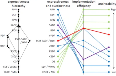
2.13 Hierarchy graph of dataflow based models. . . 45
3.1 A decimator connected to an average filter with fixed size data flows mod-eled by SDF-AP. . . 55
3.2 A decimator connected to an average filter with an infinite data flow mod-eled by SDF-AP. . . 56
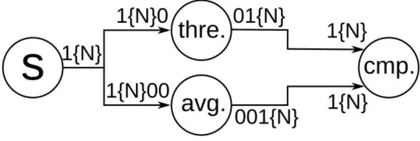
3.3 An average filter and a threshold filter in parallel, feeding a comparator modeled by SDF-AP. . . 56
3.4 The process of computing output pattern. . . 65
3.5 Simulation 1 - 3→ 5 interpolator for IP4cc. . . 68
3.6 Simulation 2 - 3→ 5 interpolator for IP5cc. . . 68
3.8 Simulation 4 - 5→ 7 interpolator for IP4cc. . . 68
3.7 Simulation 3 - 3→ 5 interpolator for IP6cc. . . 69
3.9 Simulation 5 - 5→ 7 interpolator for IP5cc. . . 69
3.10 Simulation 6 - 5→ 7 interpolator for IP6cc. . . 69
3.11 Simulation 7 - 5→ 8 interpolator for IP4cc. . . 69
3.12 Simulation 8 - 5→ 8 interpolator for IP5cc. . . 69
3.13 Simulation 9 - 5→ 8 interpolator for IP6cc. . . 70 9
3.14 Simulation 10 - 5→ 7 interpolator v2, for IP5cc. . . 70
3.15 Simulation 11 - 5→ 7 interpolator for IP3cc. . . 70
3.16 AIX4-stream - IPs using the blocking mode. . . 71
3.17 AIX4-stream - IPs using the non-blocking mode. . . 72
4.1 An graph presented by ASAP model. . . 76
4.2 An example of channels aggregation. . . 76
4.3 Consumption rates: the most favorable case and the unfavorable case. . . . 77
4.4 Consumption rates of an actor in different cases. . . 78
4.5 The flow chart of conformance checking and modification. . . 79
4.6 A graph (consistent) presented in SDF model. . . 81
4.7 A labeled graph. . . 81
4.8 A graph (inconsistent) presented in SDF model. . . 82
4.9 Building admittance pattern for Example 9. . . 87
4.10 Infinite number of choices when building an admittance pattern. . . 88
4.11 Building admittance pattern for Example 11. . . 91
4.12 An ASAP design: filtering a stereo signal. . . 93
4.13 Demonstration case: a graph of blocks for real-time image processing on an FPGA. . . 97
5.1 The flow chart of working process in BlAsT. . . 104
5.2 A demo design in BlAsT. . . 106
5.3 An example of reference file. . . 107
5.4 Parameter setting in BlAsT. . . 108
5.5 An example of implementation file. . . 109
5.6 An example of @for instruction in an implementation file. . . 110
5.7 The patterns definition for a blur filter. . . 110
5.8 An example of generated VHDL code for a top group. . . 112
5.9 An example of wheels detector design in BlAsT. . . 113
5.10 Detection of an incompatible case. . . 114
5.11 Investigating an incompatible case. . . 114
2.1 Truth table for boolean AND operation . . . 31
3.1 Characteristics of 5 → 7 and 5 → 8 interpolators . . . 68
4.1 Production counters of blocks . . . 98
4.2 Production patterns for different camera clocks . . . 99
4.3 Resources consumption with ASAP model . . . 99
4.4 Min. and max. combination of test parameters with SDF-AP model. . . 100
4.5 Test results of two examples of timings . . . 100
1 Transmutation from input pattern to input schedule. . . 58
2 Transmutation from output pattern to output schedule. . . 58
3 Transmutation from output schedule to output pattern. . . 58
4 Output pattern generation. . . 66
5 Traversal order determination. . . 83
6 Ratio checking and resampling. . . 85
7 Admittance generation. . . 90
8 Compatibility checking. . . 92
9 Pattern modification and decimation. . . 95
10 Delays calculation. . . 96
In order to help the reader, the main notions and acronyms used in this manuscript are reported here, together with a short description in English and French. They are given in their approximate order of appearance.
• SDF graph: Static Data Flow graph (graphe `a flux de donn ´ees statiques).
SDF is a model that abstracts a design with a graph composed of actors linked by channels. An Actor represents a process that consumes and produces a fixed (i.e. static) number of data during each of its executions. Data are received/sent via the channels.
SDF est un mod `ele qui abstrait un design gr ˆace `a un graphe compos ´e d’acteurs reli ´es par des canaux. Un acteur repr ´esente un processus qui consomme et produit un nombre fixe (d’o `u le mot statique) de donn ´ees `a chacune de ses ex ´ecutions. Les donn ´ees sont rec¸ues/envoy ´ees via les canaux.
• SDF-AP: Static Data Flow with Access Patterns (flux de donn ´ees statiques avec sch ´ema d’acc `es).
SDF-AP is a model that uses access patterns to describe at which clock cycles an actor consumes/produces data during a single execution. A pattern is a sequence of 1 and 0, with a length equal to the duration of the execution in clock cycles. For a given clock cycle, a 1 means that the actor consumes/produces a data.
SDF-AP est un mod `ele qui utilise des sch ´emas d’acc `es pour d ´ecrire `a quel cy-cle horloge un acteur consomme/produit une donn ´ee lors de son ex ´ecution. Un sch ´ema d’acc `es est une suite de 1 et 0, dont la longueur est celle d’une ex ´ecution en terme de cycles horloge. Pour un cycle donn ´ee, un 1 signifie que l’acteur con-somme/produit une donn ´ee.
• ASAP: Actors with Stretchable Access Patterns (Acteurs avec sch ´ema d’acc `es ex-tensible).
ASAP is a model also using access patterns. Nevertheless, patterns describe the maximum pace of consumption/production of an actor. When connected to other actors, it may receive/send data at a lower pace, which means that the pattern contains more 0 than expected: it is stretched. This model is the central contribution of this PhD.
ASAP est un mod `ele qui utilise ´egalement les sch ´emas d’acc `es. N ´eanmoins, ces sch ´emas d ´ecrivent le rythme maximum de consommation/production. Quand un acteur est connect ´e `a d’autres, il peut recevoir/envoyer des donn ´ees `a un rythme plus lent. Cela implique que le sch ´ema contient plus de 0 que pr ´evu : il est donc
´etir ´e.
• PI, PO: Number of input/output ports (nombre de ports d’entr ´ee/sortie). 15
For an actor within a graph, PI is the number of its input channels, and PO the number of output channels. The word “port” is a reference to the name used for inputs/outputs signals of a VHDL component.
Pour un acteur au seind d’un graphe, PI est le nombre de canaux entrants et PO celui des canaux sortant. Le mot “port” est une r ´ef ´erence `a celui utilis ´e pour les signaux d’entr ´ee/sortie d’un composant VHDL.
• CP, PP: Consumption/Production pattern (Sch ´ema de consommation/production). The consumption/production pattern represents the maximum pace of consump-tion/production of an actor, during one execution. For example, CP= [101] means that the actor can consume at most a data during the first and third clock cycle of its execution.
Le sch ´ema de consommation/production repr ´esente le rythme maximal de consom-mation/production d’un acteur durant son ex ´ecution. Par exemple, CP= [101] signi-fie que l’acteur peut au mieux consommer une donn ´ee lors des premier et troisi `eme cycles horloge de son ex ´ecution.
• δ: Production delay (d´elai de production).
It represents the latency of an actor, i.e. the number of clock cycles needed to produce the first result. It corresponds to the number of 0 at the beginning of PP. Il repr ´esente la latence d’un acteur, c’est- `a-dire le nombre de cycles horloge pour produire le premier r ´esultat. Il correspond au nombre de 0 au d ´ebut de PP.
• PC: Production counter (Compteur de production).
The production counter represents the number of data that must be consumed to produce a particular data. For example, PC = [2, 3] means that the actor must consume 2 data to produce the first result, and one more (thus 3) to produce the second.
Le compteur de production repr ´esente le nombre de donn ´ees qui doivent ˆetre con-somm ´ees pour produire une donn ´ee en particulier. Par exemple, PC = [2, 3] signifie que l’acteur doit consommer 2 donn ´ees pour produire le premier r ´esultat, et une de plus (donc 3) pour produire le second.
• IP, OP: Input/Output pattern (Sch ´ema d’entr ´ee/de sortie).
The input/output pattern represents what an actor really receives/produces all along its executions when it is connected to other actors. IP must be compatible with the admittance pattern (see below) so that the actor can consume and process the data correctly. In that case, OP is computed from IP, PP and PC.
Le sch ´ema d’entr ´ee/sortie repr ´esente ce qu’un acteur va r ´eellement recevoir ou produire tout au long de ses ex ´ecutions, lorsqu’il est connect ´e `a d’autres acteurs. IP doit ˆetre compatible avec le sch ´ema d’admissibilit ´e (voir ci-dessous) pour que l’acteur consomme et traite correctement les donn ´ees. Dans ce cas, OP est calcul ´e
`a partir de IP, PP et PC.
• IS, OS, PS: Input, Output, Production Schedules (Timings d’entr ´ee, sortie, produc-tion).
The input, output or production schedules are an alternative representation of the patterns. The schedule is the list of the clock cycles at which there is a 1 in the associated pattern.
Les timings d’entr ´ee, sortie ou production sont une repr ´esentation alternative des sch ´emas d’acc `es. Un timing est la liste de cycles horloge o `u apparaˆıt un 1 dans le sch ´ema associ ´e.
• AP: Admittance pattern (Sch ´ema d’admissibilit ´e).
The admittance pattern is built from the consumption pattern. If removing some 0 in the input pattern leads to the admittance pattern, they are declared to be compati-ble. It means that the actor consumes and processes correctly the input data. Le sch ´ema d’admissibilit ´e est cr ´e ´e `a partir du sch ´ema de consommation. Si en supprimant des 0 du sch ´ema d’entr ´ee, on obtient le sch ´ema d’admissibilit ´e, ils sont d ´eclar ´es comme ´etant compatibles. Cela signifie que l’acteur consomme et traite correctement les donn ´ees.
• ∆: Delay between executions (d´elai entre les ex´ecutions).
It describes the number of data that must be consumed by an actor before it can start another execution. Depending on its value and the number of 1 in the con-sumption pattern, it may lead to concurrent executions of the actor.
Il d ´ecrit le nombre de donn ´ees qui doivent ˆetre consomm ´ees par un acteur avant qu’il ne puisse ˆetre ex ´ecut ´e une nouvelle fois. Selon sa valeur et le nombre de 1 dans le sch ´ema de consommation, cela peut conduire `a des ex ´ecutions concur-rentes de l’acteur.
• Γ: Topology matrix (matrice de topologie).
It represents the relations between actors and their consumption/production on the channels of a graph. Assuming actors and channels are labeled with unique num-bers,Γi, j is the number of data consumed/produced (depending on the sing value) by actor j on channel i.
Elle indique les relations entre les acteurs et leur consommation/production sur les canaux. En supposant que chaque acteur/canal rec¸oit un num ´ero unique,Γi, j donne le nombre de donn ´ees consomm ´ees/produites (selon de signe de la valeur) par l’acteur j sur le canal i.
• q: Repetition vector (vecteur de r ´ep ´etition).
This vector only exists if all data produced by actors during a certain number of ex-ecutions are finally consumed in a finite time. It expresses the existence of a cycle. Taking into account the same labels used forΓ, qi gives the number of executions of actor i to obtain that cycle.
Ce vecteur n’existe que si toutes les donn ´ees produites par les acteurs durant un certain nombre d’ex ´ecutions sont consomm ´es dans un temps fini. Cela exprime une notion de cycle. En se basant sur la m ˆeme num ´eration de Γ, qi indique le nombre d’ex ´ecution de l’acteur i pour obtenir ce cycle.
• O: Traversal order (ordre d’analyse).
This vector gives an order to analyze the actors, for example when input pattern compatibility is checked. It ensures that all the precursors of a given actor are analyzed before itself.
Ce vecteur indique un ordre pour analyser le graphe, par exemple afin de tester la compatibilit ´e des sch ´emas d’entr ´ee. Cet ordre assure que tous les pr ´ecurseurs d’un acteur sont ´evalu ´es avant lui-m ˆeme.
• C M, PM: Consumption/Production matrix (matrice de consommatio/production). They give the number of data sent/receive between two given actors. They are used to check if sample rates of consumption/production are consistent between actors. Elles indiquent le nombre de donn ´ees envoy ´ees/rec¸ues entre deux acteurs donn ´es. Elles sont utilis ´ees pour v ´erifier que les taux de consommation/production entre deux acteurs sont coh ´erents.
• D: Downsampling matrix (matrice de r ´eechantillonage).
This matrix indicates the downsampling (i.e. the decimation rate) that must be ap-plied between two actors so that their rates of consumtion/production are consistent. Cette matrice indique le r ´e ´echantillonnage (c.a.d. le taux de d ´ecimation) `a ap-pliquer entre deux acteurs afin que leur taux de consommation/production soient coh ´erents.
• DS : Decimation schedule (Timings de d ´ecimation).
DS contains a vector for each input port of an actor. Each vector gives the clock cycles at which a decimation occurs (i.e. a valid data that is ignored).
DS contient un vecteur pour chaque port d’entr ´ee d’un acteur. Chaque vector in-dique `a quel cycles horloge une d ´ecimation doit avoir lieu (c.a.d. une donn ´ee valide ingor ´ee).
• DM: Delay matrix (Matrice des d ´elais).
DM contains the delay that must be applied to each valid value received by an actor. It may be 0. These delays allows to enforce a corect processing.
DM contient le d ´elai `a appliquer pour chaque donn ´ee valide rec¸ue par un acteur. Cela peut ˆetre 0. Ces d ´elais permettent d’assurer un traitement correct.
• BlAsT: Block Assembly Tool (Outil d’assemblage de blocs).
BlAsT is the software developped in the framework of this PhD. It allows to create FPGA designs graphically, to analyze and to modify them with the principles of ASAP. It also generates the VHDL code.
BlAsT est l’outil logiciel d ´evelopp ´e dans le cadre de cette th `ese. Il permet de cr ´eer de fac¸on graphique des designs pour FPGA, de les analyser et les modifier gr ˆace aux principes d’ASAP. Il g ´en `ere ´egalement le code VHDL.
The long journey of my Ph.D. study has finished. It is with great pleasure to express my most sincere gratitude to Prof. Michel Lenczner and Assoc. Prof. St ´ephane Domas, my supervisors, for giving me the opportunity to work on my dissertation, and for their ded-icated guidance, thoughtful advices and endless patience during the course throughout the entire process of my study. During the past three years, They have been constantly available to discuss our results and provide insightful suggestions. Without their brilliant and illuminating instructions on my research and even about the writing, this disserta-tion could not reach its present form. This dissertadisserta-tion would never have been possible without their elaborative direction and meticulous corrections.
I wish also to acknowledge the members of AND(Algorithmique Num ´erique Distribu ´ee) for the warm and friendly atmosphere in which they allowed me to work. Especially for the helps from Prof. Rapha ¨el Couturier and my colleague Yousra Ahmed Fadil, Amor Lamar, Nesrine Khernane and Ali Kadhum Idrees both in life and study. I will never forget all the colleagues: Jean-Franc¸ois Couchot, Mourad Hakem, Gilles Perrot, Michel Salomon, Jean-Claude Charr, Karine Deschinkel, Arnaud Giersch, Abdallah Makhoul, Fabrice Ambert, Christophe Guyeux, Mohammed Bakiri, Joseph Azar, Gaby Boutayeh, Zeinab Fawaz, Christian Salim, Carol Habib, Anthony Nassar and Ahmed Badri Muslim Fanfakh.
I would further like to give my gratitude to the financial support from the program of China Scholarships Council (CSC), and to UBFC where I did my dissertation.
My sincere thanks also goes to my friends that I passed an amazing journey with them in France. I will never forget the beautiful moments I shared with you: Ruifeng Zhu, Yan Wang, Jie Qiu, Chunjie Huang, Chaoyue Chen, Hui Shang, Renfei Han, Zhao Zhang, Dongxue Lu, Chen Song, Jianding Guo, Yingchun Xie, Rongrong Liu, Jian Zhang, Tao Jiang, Hailong Wu, Mengli Yin, Lei Zhang, Daming Zhou, Bei Li, Yu Wu, Jinjian Li, Jin Wei.
I would also like to express my thanks to the high speed development of China and the fast growing of real estate prices, which have been encouraging me to non-stop hard working.
Finally, I wish to take this opportunity to express my appreciation and thanks to all my family for the emotional support. I would especially like to thank my parents who provide me the mental support and encouragement to explore the unknowns. Thanks especially to my wife Shuyi for her love. The future will be much better.
I
NTRODUCTION
1.1/
G
ENERALI
NTRODUCTIONWith the development of electronic industry, a growing number of projects require real-time streaming applications on embedded platforms. These comprise increasingly high hardware and timing constraints, which leads to the use of FPGAs (Field Programmable Gate Arrays). Usually, the designer should have a good knowledge of programming with VHDL or Verilog HDL. Unfortunately, only specialists can do it, because this needs a lot of training and practices to master the skill. Furthermore, even for specialists, the process of development is quite time consuming. Therefore, how to develop a tool to help non-expert users working on FPGA is a promising but challenging work.
In order to manage the ever-increasing size and complexity of designs, the abstraction is gradually more and more essential. As a result of a trend called “raising the level of abstraction”, the developer can focus on the design at higher-level properties that mat-ter most, which helps to avoid being bothered by the lower-level details. This is true in both software programming and hardware design, which have historically evolved toward higher-level languages and models. For software, programming languages have evolved from process-oriented assembly to object-oriented programming, such as C++ and Java. In the meanwhile, coming with the advances of chips and EDA tools functionalities, hard-ware design has evolved from basic logic elements transistor and gate layout to logic synthesis and high-level synthesis.
In another aspect, coping with large and complex systems, current hardware design practice often relies on integration of components. Although it makes hardware develop-ment much easier by allowing modularization and component reuse, because of a lack of support with rigorous methodologies, theories and tools are still managed in a mostly ad-hoc process. Some disturbing troubles or difficulties may be caused by the informal description documents of components. For example, designers can only get descriptions of structural but non-behavioral specifications in IP-XACT, which are usually incomplete. Moreover, the ability to read the files in English is a prerequisite.
Not only some models but also some tools have emerged in recent years, based on the concept of HLS (High Level Synthesis). They can make transformation in high-level languages, such as C and VHDL. These tools are increasingly effective but limited to low stress applications. Other tools exist, such as Simulink / HDL coder based chaining function blocks [65, 64]. This is the easiest way to create, debug and test a processing via simulation. Nevertheless, the results are seldom applicable when actually implemented
in FPGAs.
1.2/
M
OTIVATION ANDO
BJECTIVESIn general, the existing tools suffer from two flaws. One is that they do not take the physi-cal characteristics of the target architecture of the application into account, including that of the selected FPGA. The other one is that they do not check whether a data stream is processed correctly by the chain, besides creating many test-benches, which is tedious and time consuming for the developer. In fact, these tools can neither analyze the pro-cess of a data stream when it passes through the propro-cessing graph nor test whether the blocks are actually able to produce the expected outcomes based on the entries and the selected target FPGA. Therefore, they are not suitable to produce applications in real-time environment and high hardware constraints.
These problems have been partially addressed in a previous thesis [32] that proposed a software environment named CoGen. It allows to create chains of blocks to process video streams (or similar ones), and check the capacity of each block to process the stream it receives. Finally, it was able to produce VHDL code for some FPGAs.
The primary objective of this dissertation is to generalize these results to an acyclic graph of blocks, by providing a model of them that allows to determine mathematically the correctness of the result, and thus without launching complex simulations. Every component used in FPGAs is regarded as a block. If the inputs and outputs of connected blocks can be approved compatible, the designed system can be implemented on an FPGA by hardware design languages (VHDL or Verilog HDL). But if the analysis result is negative, algorithms for modifying the design are needed. This is another objective of this thesis. After some modifications, some designs can be implemented on hardware and the correct designs can be derived from our approaches by algorithms. Otherwise, the designs are regarded as unable to be implemented correctly on FPGAs.
The final goal of this thesis is to develop a software tool which can produce VHDL code from a graph of functional blocks. It can do far more than existing ones based on the same concepts. One major new possibility, based on our models and algorithms, is to check whether the result will be correctly carried out by the proposed model and algorithms for a given input stream. The production of final VHDL code is made automatically by assembling previously developed components. This process is called block assembly. Then, the blocks are able to self-schedule their executions because they know the status of executions. Thus, users without VHDL programming skills are able to generate correct code by assembling blocks.
1.3/
C
ONTRIBUTIONS OF THIST
HESISIn this dissertation, we concentrate on the study of the static analysis of block and graph models and the software tool that can help non-expert users for automatic design of FPGA implementations correctly. The main contributions are summarized as follows:
i) The limitations of existing SDF based models, in particular those of the SDF-AP model, are described and illustrated by the analysis of characteristic examples. The
two most common problems encountered in block assembly implementations are the production of incorrect results and the infinite growth of buffer size.
ii) We propose a new model called Actors Stretchable Access Patterns (ASAP) that describes the hardware behaviors as efficiently and precisely as possible. This is a novel way to address the scheduling problem of actors dedicated for FPGA archi-tectures. It opens the possibility to determine the execution correctness mathemati-cally without launching complex simulations. It can not only model actors’ behaviors properly, but also avoid the above mentioned drawbacks. Algorithms of transmuta-tions of the patterns and corresponding schedules and output pattern generation are also provided.
iii) We investigate strategies and related algorithms to analyze and schedule graphs of systems. The correctness of the designed systems can be analyzed by a series of algorithms, such as sample rate checking and pattern compatibility checking. Using the proposed ASAP model, the rate decimation and actor’s input pattern modifica-tions are applied when a correctness failure is detected. This increases the number of possible real FPGA implementations covered by the block assembly method. iv) A software tool based on the concept of functional block graph is also developed.
It is called BlAsT (Block Assembly Tool) and aims to compensate the drawbacks of other tools based on the same concepts, as for example Simulink + HDL coder. In BlAsT, the proposed ASAP model and related algorithms are used to check that for a given input stream, whether the system can produce a correct result and finally generate VHDL code directly usable on a real FPGA-based board. Otherwise, the tool determines the required decimations and modifications on the graph automat-ically. It makes a user without any programming skills able to make designs on FPGAs thanks to the friendly graphic interface.
1.4/
T
HESISO
UTLINEThe dissertation is organized as follows: the next chapter is a review of the related litera-ture dedicated to models for static analysis and related tools oriented to FPGA implemen-tation. A brief analysis of each model and tool is also discussed. Chapter 3 discusses the main limitations of the SDF-AP model and presents the principles of the proposed analysis model: Actors with Stretchable Access Patterns (ASAP). Both basic algorithms for pattern generation and transmutation are given together. Chapter 4 introduces the strategies to analyze a design modeled with the ASAP principles. Algorithms achieving this analysis are given in detail with examples. Furthermore, the proposed principles are verified to be feasible and efficient by some metrics and tests on realistic cases. Chapter 5 describes our EDA tool BlAsT developed based on the concept of block assembly, the proposed ASAP model and related approaches. Functionalities and the methods for us-ing the tool are illustrated by a real application. Finally, the conclusions of the work and some perspectives are given in the last chapter.
S
CIENTIFIC
B
ACKGROUND
S
UMMARY OF
B
IBLIOGRAPHY
2.1/
I
NTRODUCTIONHardware devices are widely used nowadays both in scientific environment and daily lives of common people. Among the different types of architectures, FPGAs have become indispensable choices for designers. Regardless of the relative high price, they really improve the reliability and the integration of systems, and they are especially suitable for small batch systems. Modern embedded systems often execute parallel applications. For instance smartphones have four or more processors and several applications can be run for different purposes simultaneously. Thus, there are many expectations for the systems, such as a robust behavior, stable performances and less resource consumption especially minimal energy cost for battery limitation, etc [19, 79]. Thanks to the high degree in integration, it is possible to design complex and large size systems. This leads to the conception of Multi-Processor Systems-on-Chips (MPSoCs). Some discussions about related theories and techniques can be found in [44, 78].
The abstraction of systems allows the designers to deal with large and complex sys-tems. Cooperating with the abstraction, in the meanwhile, the reusable components work as functional blocks in different levels play an important role in hardware design. Both of them help a lot for FPGA design and yield more powerful FPGA applications. But pro-gramming MPSoCs is a challenging work, especially timing problems may be caused by the interaction between the components [63]. The design of the requisite communication and the control logic to connect the blocks are still made manually which is time con-suming and error-prone. Designing hardware systems is usually done by taking system abstraction and usable components into account to meet the performance requirements. In practice, in order to chose the components to build a system correctly, the real-time en-vironment and hardware constraints should be taken into consideration at the same time. Then, designers must deal with the interfaces of blocks in a manual way. Thus, they are usually faced with low-level control and timing artifacts. Even when all parts of systems are already built, designers still need to spend considerable time to debug [20]. Therefore, it is really hard to design MPSoCs on FPGAs. Some key issues regarding MPSoC design and programming is discussed in [62]. This includes the number of processors, interpro-cessor communications, concurrency, memory hierarchy, platform scalability, models of programming and control, etc. Although there are some commercial ESL and EDA tools which can provide help to designers, such as Xilinx ISE, they are still like the IP industry requiring to offer large components of the solution.
The question of whether it is possible to find a way to automatically reduce the 27
complexity of creating designs still remains. Many researchers have worked on it for a long time. With the efforts of researchers, series of models have been proposed. Nowadays, designing hardware often involves model based analysis and techniques [67, 82, 72, 61, 36, 10], and the related tools have also been developed, which can help to check the correctness of systems and give performance evaluations.
The basic problem is discussed in [88] with a vivid name as the glue design problem. An abstract model of hardware systems is provided to analyze the system correctness and performance properties. There are also other models dealing with the similar prob-lems since 30 years ago, but surprisingly none of them described the hardware behavior precisely. Therefore, important information about system are omitted yielding rough sys-tem descriptions and resulting in either defensive or aggressive analysis results.
As for tools, there has been an increasing interest in the development and use of standard formats for system structure and IP configuration parameters. Among them, XML-based formats and data flow interchange format are widely used in the software tools development. But the core part to analyze the performance of the system is the model. Therefore, the analysis results of tools based on existing models can be seldom used directly and correctly.
It is promising to find a model that can describe the behaviors of hardware exactly and capture the properties of systems faithfully. If such a model is achieved, the related analysis results can be used in hardware design directly, especially for FPGAs. A software tool based on such a model will be more promising.
2.2/
F
IELDP
ROGRAMMABLEG
ATEA
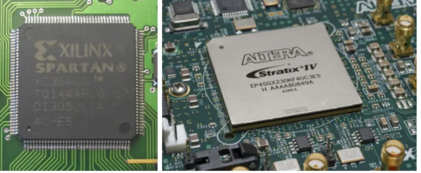
RRAYSField programmable gate arrays (FPGAs) are reprogrammable silicon chips. In 1985, the first FPGA was invented by Ross Freeman, the cofounder of Xilinx. In fact, FPGAs combine the best parts of application-specific integrated circuits (ASICs) and processor-based systems. This why FPGA chips are adopted across all industries. FPGAs provide hardware-timed speed and reliability, but they do not require high volumes to justify the large upfront expense of custom ASIC design. Figure 2.1 shows two FPGA chips pro-duced by Xilinx (on the left) and Altera (on the right), which are the current FPGA market leaders and long-time industry rivals. Together, they control over 80 percents of the world-wide market.
Figure 2.1: FPGA chips produced by Xilinx and Altera.
processor-based system, but it is not limited by the number of available processing cores. Unlike processors, FPGAs are truly parallel in nature, so different processing operations do not have to compete for the same resources. This makes it possible for designers to get around the basic limitations of sequential processors. Each independent processing task is assigned to a dedicated section of the chip, and can function autonomously with-out any influence from other logic blocks. As a result, the performance of one part of the application is not affected when adding more processing.
2.2.1/ COMPONENTS OF FPGAS
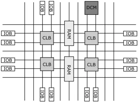
Until now, most of the FPGAs are based on look up tables (LUTs) technique. Every FPGA chip is made up of a finite number of predefined resources. Configurable logic blocks (CLB) are the basic unit of FPGAs. As shown in Figure 2.2, it works with programmable interconnects to implement a reconfigurable digital circuit, I/O blocks (IOB) to allow the circuit to access the outside world, embedded block RAM to make it more flexible in applications and digital clock management modules (DCM).
DCM CLB CLB CLB CLB IOB IOB IOB IOB IOB IOB IOB IOB IOB IOB
IOB IOB IOB IOB
RAM
RAM
Figure 2.2: The different parts of an FPGA.
Generally, the metrics to evaluate FPGA resource specifications include the number of configurable logic blocks, the number of fixed function logic blocks such as multipliers and the size of memory resources like embedded block RAM. The parts shown in the above figure are typically the most important in FPGA chips. When selecting FPGAs for a particular application, these metrics must be taken into consideration.
The CLBs, sometimes referred to as slices or logic cells, are made up of two basic components: flip-flops and lookup tables (LUTs). Various FPGA families differ in the way flip-flops and LUTs are packaged together, so it is important to understand the principle of flip-flops and LUTs operation.
2.2.1.1/ FLIP-FLOPS
Flip-flops are binary shift registers used to synchronize logic operations and save logical states between clock cycles within an FPGA circuit. On every clock edge, a flip-flop latches the 1 (TRUE) or 0 (FALSE) value on its input and holds that value constant until the next clock edge. As shown in Figure 2.3, a flip-flop has an input, an output and a clock signal.
Output Input
Clock
Figure 2.3: The symbol of flip-flop.
2.2.1.2/ LOOKUPTABLES (LUTS)
Much of the logic in a CLB is implemented using very small amounts of RAM in the form of LUTs. Figure 2.4 shows a 4-input LUT. It is easy to assume that the number of system gates in an FPGA refers to the number of NAND gates and NOR gates in a particular chip. But, in reality, all combinatorial logic (ANDs, ORs, NANDs, XORs, and so on) is implemented as truth tables within LUT memory. A truth table is a predefined list of outputs for every combination of inputs.
Output Input 1 Input 4 Input 3 Input 2
LUT
Figure 2.4: An 4-input LUT.
The Boolean AND operation, for example, is shown in Figure 2.5 and the correspond-ing truth table for the two inputs of an AND operation is shown in Table 2.1.
Output
Input 1
Input 2
&
Figure 2.5: Boolean AND operation.
2.2.1.3/ MULTIPLIERS ANDDSP SLICES
Figure 2.6 shows a multiply function for the simple task of multiplying two numbers, which can get extremely resource intensive and complex to implement in digital circuitry. This
Table 2.1: Truth table for boolean AND operation
Input1 Input2 Output
0 0 0
0 1 0
1 0 0
1 1 1
is illustrated in Figure 2.7 that shows the schematic drawing of one way to implement a 4-bit by 4-bit multiplier using combinatorial logic. When it comes to multiplying two 32-bit numbers, it ends up with more than 2000 operations. For this reason, FPGAs have prebuilt multiplier circuitry to save on LUT and flip-flop usage in math and signal processing applications.
x*y
x
y
x
Figure 2.6: Multiply function.
Figure 2.7: Schematic drawing of a 4-bit by 4-bit multiplier.
Many signal processing algorithms involve keeping the running total of numbers being multiplied, and, as a result, higher-performance FPGAs like Xilinx Virtex-5 FPGAs have
prebuilt multiplier-accumulate circuitry. These prebuilt processing blocks, also known as DSP48 slices, integrate a 18 × 18 bits multiplier with adder circuitry.
2.2.1.4/ BLOCKRAM
Memory resources are another key specification to consider when selecting FPGAs. User-defined RAM, embedded throughout the FPGA chip, is useful for storing data sets or passing values between parallel tasks. Their size and number depends on the FPGA family and model. For example, a Spartan 6 LX100 integrates 536 RAM blocks of 9Kbits. There is still the option to implement data sets as arrays using flip-flops; however, large arrays quickly become expensive for FPGA logic resources. A 100-element array of 32-bit numbers can consume more than 30 percent of the flip-flops in a Virtex-II 1000 FPGA or take up less than 1 percent of the embedded block RAM. Digital signal processing algo-rithms often need to keep track of an entire block of data, or the coefficients of a complex equation, and without on-board memory, many processing functions do not fit within the configurable logic of an FPGA chip.
The inherent parallel execution of FPGAs allows for independent pieces of hardware logic to be driven by different clocks. Passing data between logic running at different rates can be tricky, and on-board memory is often used to smooth out the transfer using first-in-first-out (FIFO) memory buffers.
2.2.2/ FPGA DESIGN AND TOOLS
With the understanding of the fundamental FPGA components, the advantage of imple-menting a design in hardware circuitry can be seen clearly: it allows improvements in execution speed, reliability, and flexibility. However, in the process of FPGA design some trade-offs should be made based on an FPGA for the processing and I/O connectivity in a system.
For FPGA design, the designer defines digital computing tasks in software using devel-opment tools and then compile them down to a configuration file or bitstream that contains information on how the components should be wired together. Although there are many development tools, the challenge in the past with FPGA technology was that the low-level FPGA design tools could be used only by engineers with a deep understanding of digital hardware design. However, the rise of high-level synthesis (HLS) design tools, such as Simulink developed by MathWork and the NI LabVIEW system design software, changes the rules of FPGA programming in some degree.
2.2.2.1/ THEDESIGNFLOW
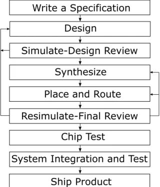
As the design is the main part of FPGA implementations, it is necessary to talk about the entire process. Figure 2.8 shows the design flow of hardware devices, not only for FPGA but also for others, such as ASIC and CPLD. Following the steps in the design flow can guarantee the best chance to get a correct prototype of the designed system.
Design
Simulate-Design Review
Synthesize
Place and Route
Resimulate-Final Review
Chip Test
System Integration and Test
Write a Specification
Ship Product
Figure 2.8: The flow chart of FPGA design.
Writing a specification is the first step. This plays a quite important role as a guide for designers to understand the entire design and choose the proper devices. It allows to de-sign the correct interface to the rest of the pieces of the chip. It also helps to save time and avoid misunderstanding. The following information should be included in a specification:
• An external block diagram showing how the chip fits into the system. • An internal block diagram showing each major functional section.
• A description of the I/O pins, including output drive capability and input threshold level.
• Timing estimates, including setup and hold times for input pins, propagation times for output pins and clock cycle time.
• Estimated gate count. • Package type.
• Target power consumption. • Target price.
• Test procedures.
With the specification, the designer can find the best vendor with a technology and structure that best meets the requirements of the project. At this point, a design entry method should be chosen. Generally speaking, for small chips, schematic entry is used,
especially if the designer is familiar with the tools. But for large designs, a hardware de-scription language (HDL) such as VHDL or Verilog HDL is used for its portability, flexibility, and readability. When using a high level language, synthesis software is required to “syn-thesize” the design. This means that the software creates low level gates from the high level description. Thus, at the same time, the designer should choose a synthesis tool, which is important since each synthesis tool has recommended or mandatory methods of designing so that it can work properly.
After knowing the aim of the system to be designed and get all the preparation ready, it comes to the core step designing the chip. This is the most essential and difficult work for hardware design, which mainly involves programming using the chosen hardware description language.
In order to get the correct functionality, simulation is a process while the design is being done. Small sections of the design should be simulated separately before hooked up to larger sections. There should be many iterations of design, simulation and review for a final system.
When the design is finished, the designer should use the synthesis software to syn-thesize the chip. It involves translation of the register transfer level (RTL) design into a gate level design which can be mapped to logic blocks in the FPGA. And then, the design should be programmed into chip, which is called place and route. The design results in a real layout for a real chip.
After layout, another simulation is necessary to check whether the real chip goes on well and the results agrees with the predicted ones. If every part of the system performs correctly, finally, system integration and system testing is carried out to insure all parts of the entire system work correctly together. When there is no problem in the system, the product of the design is obtained at last.
2.2.2.2/ TRADITIONALDESIGNTOOLS
In the whole process of hardware design, the tools used are critical to the design. Through the first 20 years of FPGA development, hardware description languages (HDLs) such as VHDL and Verilog evolved into the primary languages for designing the algorithms running on FPGA chips. These low-level languages integrate some of the benefits offered by other textual languages taking into account that on an FPGA, a circuit is architectured. The resulting hybrid syntax requires signals to be mapped or connected from external I/O ports to internal signals, which ultimately are wired to the functions that house the algorithms. These functions execute sequentially and can reference other functions within the FPGA. However, the true parallel nature of the task execution on an FPGA is hard to visualize in a sequential line-by-line flow. HDLs reflect some of the attributes of other textual languages, but they differ substantially because they are based on a dataflow model where I/O is connected to a series of function blocks through signals.
To verify the logic created by an FPGA programmer, it is a common practice to write test benches in HDL to wrap around and exercise the FPGA design by asserting inputs and verifying outputs. The test bench and FPGA code are run in a simulation environment that models the hardware timing behavior of the FPGA chip and displays all of the input and output signals to the designer for test validation. The process of creating the HDL test bench and executing the simulation often requires more time than creating the original
FPGA HDL design itself.
Once an FPGA design using HDL is created and verified, it needs to be fed into a compilation tool that takes the text-based logic and, through several complex steps, syn-thesizes the HDL down into a configuration file or bitstream that contains information on how the components should be wired together. As part of this multistep manual process, it often requires a mapping of signal names to the pins on the FPGA chip that is used.
Ultimately, the challenge in the design flow is that the expertise required to program in traditional HDLs is not widespread, and as a result, FPGA technology has not been accessible to the vast majority of engineers and scientists.
2.2.2.3/ HIGH-LEVEL SYNTHESIS DESIGN TOOLS
Thanks to the emergence of graphical HLS design tools, such as LabVIEW, some of the major obstacles of the traditional HDL design process are removed. The LabVIEW programming environment is distinctly suited for FPGA programming because it clearly represents parallelism and data flow, so users who are both experienced and inexperi-enced in traditional FPGA design processes can leverage FPGA technology. In addition, existing VHDL codes can be used to be integrated within designs. The Intellectual Prop-erty (IP) can be used, among which IP blocks from native and third-party sources are widely used. The most familiar IP sources are Xilinx CoreGen [40], National Instruments LabVIEW FPGA [42], and the OpenCores library [1].
Then to simulate and verify the behavior of a FPGA logic, LabVIEW offers features directly in the development environment. Without knowledge of the low-level HDL lan-guage, one can create test benches to exercise the logic of the design. In addition, the flexibility of the LabVIEW environment helps more advanced users model the timing and logic of their designs by exporting to cycle-accurate simulators such as Xilinx ISim.
2.2.3/ ANALYSIS
The adoption of FPGA technology continues to increase as higher-level tools such as LabVIEW and Simulink, the standard microprocessor, and the FPGA RIO architecture are making FPGAs more accessible. It is still important, however, to look inside the FPGA and appreciate how much is actually happening when block diagrams are compiled down to execute in silicon. Comparing and selecting hardware targets based on flip-flops, LUTs, multipliers, and block RAM is the best way to choose the right FPGA chip for your application. Understanding resource usage is extremely helpful during development, especially when optimizing for size and speed. The existing HLS design tools deliver new technologies that convert graphical block diagrams into digital hardware circuitry, but they may lead to unusable results or resources waste when actually implement in FPGAs for some limitations of the analysis models. They are either defensive or aggressive, even ignoring some important characteristics. Thus, there are much room to improve the high-level synthesis tools to make hardware design easier.
2.3/
M
ODELS FORS
TATICA
NALYSISIn order to improve the tools for hardware design, we should try to remove the obstacles for designers. For the implementation of complex systems, what is the most difficult thing for designers? It is obvious that when dealing with a single processor system, every com-ponent executes sequentially, which can be built easily. Therefore, it is concurrency that makes it complex [13, 34]. In order to solve this problem, some models are proposed and have shown to be effective. Among them, Synchronous (or Static) Data Flow (SDF) are widely developed and used, notably for digital signal processing applications imple-mented on parallel hardware. This model was introduced by Lee and Messerschmitt in the founding article [55]: “Data Flow is a natural paradigm for describing DSP applica-tions for concurrent implementation on parallel hardware” in 1987. This remark was done when the first FPGAs emerged but thirty years later, even if FPGAs are far more powerful and the field of applications much larger than DSP, the same problem occurs: how to build a hardware design by connecting blocks so that it produces correct results? Indeed, since hand-coding a whole design in VHDL is a very fastidious and time consuming task, describing it with a Data Flow Graph, composed of functional blocks that consume and produce data requires less efforts. Nevertheless, this way leads to two main problems to be solved:
• Finding the best conditions under which the graph produces correct results.
• Transfer the model to a real and functional implementation (e.g. in VHDL) for a chosen architecture.
The first problem has been investigated for different models, all based on the original one presented in [55] and [59] named Synchronous Data Flow (SDF). They all rely on the fact that the number of data consumed and/or produced during the execution of a block is fixed and known a priori. The execution time is also in the same case. The discus-sion of the possibility to make static analysis is argued in [4, 5, 50, 51]. Compared with Finite State Machine (FSM) [30], it leads to a simpler method in most cases. Although, FSMs abstracts hardware properties at a high level, it causes the problem known as state explosion problem [91].
A comprehensive survey on concurrent models of computation can be found in [56]. Prior research has shown that data flow and its variants are proposed to capture the task and data parallelism in streaming applications.
2.3.1/ SYNCHRONOUS DATA FLOW
2.3.1.1/ PRINCIPLES
The Synchronous Data Flow is a model to compute the operation of infinite streams of data. This model is described mathematically as a directed graph, in which nodes rep-resent actors and edges denote inter-actor communication of data. These edges are usually called channels, which connect actors with ports. This means that, in an SDF model, data are passed in the form of tokens among actors linked by channels. The model can be used to analyze processing chains of data in a system, which is the same as Petri nets [69]. The execution (or firing) of actors consumes tokens on input ports,
and in the meanwhile, produces new tokens on output ports. Thus, the number of tokens consumed and produced in a firing (named as consumption and production rates, respec-tively) should be fixed and pre-specified at design time. If the rates in an SDF graph are not the same, it is named multi-rate graph, otherwise it is homogeneous [57, 81].
Let us take an SDF model of a Source-Downsampler for example, which is shown in Figure 2.9. A 3:1 decimation downsampler actor D with one input port and one output port would consume three tokens from the source actor S via the channel C. In fact, there is a buffer to temporarily store produced tokens. When S fires, the execution lasts for two cycles (marked as ET in the figure) and at the end it produces one token. For D, the execution lasts for four cycles and during the first three cycles it consumes three tokens from the input port and at the end produces one token to the output port. It is mandatory that S must execute three times, so that D can consume three tokens (polled from the buffer) for its own execution. With the rates specified statically, it can be analyzed to verify properties such as consistency of production and consumption rates and to ensure that enough communication buffer space is allocated for correct execution. From this process, it guarantees decidability of main model properties: existence of deadlock-free and memory-bounded infinite computation, throughput, latency, and execution schedule [7, 73]. The expressiveness of SDF model capturing streaming applications naturally, coupled with its strong compile-time predictability properties, has been widely used for specifying embedded real-time applications in the domains of digital signal processing, such as DSP and FPGA hardware designs.
1
3
1
s
D
ET=2
ET=4
C
Figure 2.9: A Source-Downsampler presented by SDF.
Once the number of needed tokens is available on the input channels and enough vacant space appears on its output channels to store the tokens it will produce, the SDF model can be executed in a self-timed manner [84]. An actor reads its inputs from the respective buffers in the order in which the input tokens were produced and put into the buffer, and outputs its tokens to its production buffers. Typically, the buffers used between actors are FIFOs (First In, First Out). Handshaking is often used to implement the self-timing: an actor stalls until necessary resources (both input tokens and output space) are available, and its neighbors inform it when necessary inputs have been produced or output space has been released.
Static scheduling is applicable with SDF models. Without execution, SDF actors can be statically scheduled according to the information of consumption and production rates. The number of data tokens produced or consumed on each input and output port is specified a priori. Lee and Messerschmitt also present necessary conditions for static scheduling programs described in SDF graphs onto processors (single or multiple) in [7]. Self-timed implementations are also widely used, for a long time, which was considered as the best approach for data flow based models [53]. However, sometimes it is needed to support multiple applications running on a single system without prior knowledge of the properties of the applications at design-time. Under this circumstance, run-time schedul-ing approaches are needed as explained in [47].
2.3.1.2/ ANALYSIS
The SDF model is usually used to describe the abstract of hardware components [37, 14]. With the efforts of researchers, some efficient algorithms appeared, which can be used to compute performance metrics of SDF model, such as throughput, buffer sizes, as well as execution schedule. It has been investigated that for analyzing the timing behavior of applications, using the standard SDF model is a common practice to associate worst-case execution time models [39, 68, 75, 96, 95]. These timing information makes it possible for static analysis of SDF model. Moreover, it can provide mapping solutions to specific platforms under resource and performance constraints. These models have been applied to capture behavior of SDF actor executions for software and hardware implementations. However, losing information about the precise timing of consumption and production of tokens by an actor during a firing cycle is the main drawback of timing models. When using SDF models to analyze hardware implementation behavior, this problem is more obvious. For hardware IP blocks, data tokens should be delivered to them at precise clock cycles. But for SDF model, it can only describe the number of needed tokens and produced during an execution. This loss of exact timing information in SDF model leads to more latency and resource usage than necessary and finally results in sub-optimal analysis and implementations. Thus, the results are usually conservative.
We can take a simple design for example. Assume a producer A is connected to a consumer B. A fires and produces one token per clock cycle, and each execution of B lasts for six clock cycles and consumes six tokens per firing. But this behavior of implementing can not be captured effectively by SDF timing model. The SDF model assumes that an actor should wait to execute until there are sufficient tokens available at the inputs. For this example, the IP block of B needs six tokens in six consecutive clock cycles. Thus, B cannot fires until A completes six firings and produces six tokens. It results in the usage of a FIFO between A and B, the size of which should be at least six. And, B can execute only after the buffer has collected six tokens from A. It is obvious that this is a valid implementation, but the result is sub-optimal in terms of throughput and allocation of buffer resources. In practice, this example can be achieved by a better implementation using only a FIFO of size one.
The above problem leads to a main question that when actors can start their firing. An obvious answer to reach maximal throughput is as soon as possible, as the timed actor interface theory “the earlier the better” as Geilen proposed in [23]. But SDF model based schedules, not only self-timed but also statically scheduled [84], share one key characteristics-the actors do not execute until all necessary inputs are available and all required output space are free. Because it takes time to create tokens and fill output FIFOs, actors are guaranteed to be stalled some portion of the time while one of those two processes is going on. Although there are some run-time scheduling algorithms, due to the fact that they assume independent periodic or sporadic tasks, such simple task model is not usable for modern embedded systems. Basically, it may lead to infinite buffers. Thus, we have to come back to solve the problem mentioned above. In order to compute a valid and optimal schedule with finite buffers, some assumptions should be set:
• Tokens are all produced at the end of the executions, in a single “shot”. • These tokens are stored in a buffer, the size of which should be big enough.
• Tokens used as inputs stay in the buffer until the end of the execution.
These assumptions yield a model quite distant from the behavior of real design in VHDL. Indeed, output data are produced sequentially, sometimes in the middle of the execution. Furthermore, such a buffer is more complicated than a classical FIFO since a block can ask for tokens without flushing them from the buffer immediately, which is like a mix of FIFO and memory.
2.3.2/ CYCLO-STATICDATA FLOW
2.3.2.1/ PRINCIPLES
In the middle of 1990’s, Bilsen and Engels and al. introduce a model named Cyclo-Static Data Flow (CSDF) for system analysis, which makes improvement based on SDF by breaking a firing of actor into finer-grained phases. Generally speaking, CSDF makes up the shortcomings in some degree. It allows the consumption or production rates of an actor to vary periodically according to the given cyclic pattern. Thus, the consumption and production of tokens are specified for each phase. For CSDF model, every firing of an actor is refined to correspond to a phase, which is different from the firing of an actor for SDF model. The authors give the necessary and sufficient conditions for the possibility of a static schedule of a CSDF graph and details of methods for a static analysis for a system in [16, 9, 8].
In order to illustrate the CSDF model more clearly, the same example shown in Figure 2.9 can be expressed by CSDF model in Figure 2.10. The execution time of S is two, so it is presented as two phases, each taking one clock cycle to execute: in phase 1, S produces nothing; in phase 2, it produces one token. Similar as S, D contains four phases in one firing, also taking one cycle for each: in first three phases, D consumes one token in each phase and produces nothing; in phase 4, D consumes nothing and produces one token. Compared with SDF model, it makes the schedules of firings more efficient by shortening the waiting times for the needed tokens. Moreover, Thomas and al. made their efforts to express a transformation from CSDF graphs to SDF graphs. Thus, some of existing SDF scheduling techniques can be used in CSDF model. But it is not always feasible for every case. This transforming sometimes introduces deadlock. The detail comparison is discussed in [71].
(0,1) (1,1,1,0)
(0,0,0,1)
s
D
ET=2 (1,1)
ET=4 (1,1,1,1)
Figure 2.10: A Source-Downsampler presented by CSDF.
2.3.2.2/ ANALYSIS
CSDF model refines the unit of firing to phase, which is much smaller than original exe-cution of actor and makes the latency of scheduling shorter. It does not need to wait for