HAL Id: hal-03060192
https://hal.archives-ouvertes.fr/hal-03060192
Submitted on 13 Dec 2020
HAL is a multi-disciplinary open access archive for the deposit and dissemination of sci-entific research documents, whether they are pub-lished or not. The documents may come from teaching and research institutions in France or abroad, or from public or private research centers.
L’archive ouverte pluridisciplinaire HAL, est destinée au dépôt et à la diffusion de documents scientifiques de niveau recherche, publiés ou non, émanant des établissements d’enseignement et de recherche français ou étrangers, des laboratoires publics ou privés.
Nanomaterials for Photovoltaic Conversion
Abdelilah Slaoui, Daniel Lincot, Jean-François Guillemoles, Ludovic Escoubas
To cite this version:
Abdelilah Slaoui, Daniel Lincot, Jean-François Guillemoles, Ludovic Escoubas. Nanomaterials for Photovoltaic Conversion. Wiley-VCH Verlag GmbH & Co. KGaA, 2017, �10.1002/9783527696109�. �hal-03060192�
1
Nanomaterials for Photovoltaic Conversion
Abdelilah Slaoui 1, Daniel Lincot 2 ,
Jean François Guillemoles2,4, Ludovic Escoubas3
1Laboratoire des Sciences de l’Ingénieur, de l’Informatique et de l’Imagerie (Icube) - UMR CNRS-UdS, 23 rue du Loess, F-67037 Strasbourg , France
2Institut de Recherche et Développement sur l’Energie Photovoltaîque (IRDEP) - UMR CNRS-EDF-Chimie paristech, EDF R&D, 6 Quai Watier, F-78401 Chatou, france
3Institut Matériaux Microélectronique Nanosciences de Provence (IM2NP) – UMR CNRS- Aix-Marseille University, Campus de Saint-Jérôme, Avenue Escadrille Normandie Niemen , F-13397 Marseille, France
4, NextPV, LIA CNRS-U. Bordeaux-U. Tokyo, RCAST 4-6-1 Komaba, Meguro Ku, Tokyo, 153-8904 Japan
Abstract :
This chapter provides an overview on the concepts, materials and devices that involve nanoscience for photovoltaics. First, the general basics of photovoltaics in terms of principle and technologies will be presented. Then, the features specifically associated with the use of nanomaterials in current and future photovoltaic devices will be developed. The optical effects (quantum confinement, photonics, plasmonics), electrical effects (work function) and geometrical effects (interpenetrating structures) - which are intrinsic to nanomaterials - will be described at theoretical and experimental levels. Properties of solar cells devices involving nanomaterials such as dye and organic cells, ultrathin cells implementing metal nanostructures, new concept based cells (up and down conversion, intermediate band cells, multiexciton generation, hot carriers …) will be presented.
2
1- Introduction
Since its emerging in 1954, the field of photovoltaics, direct sunlight-electricity conversion phenomenon, has been closely associated with a class of semiconductors, basically silicon, IIIV semiconductor compounds (GaAsbased), II -VI such as CdTe, or more recently I-III--VI2 such as Cu(In,Ga,S)Se2 noted CIGS. The
associated photovoltaic cells are based on concepts derived from p-n junctions. The absorbing materials consist in either thick to thin (50 – 300 m) silicon wafers or single or stack of micrometers thick (0,5 – 2 m) layers for other inorganic materials1.
More recently, extensive studies have shown that nanochemistry and nanomaterials can provide numerous opportunities for a new generation of photovoltaics with high solar energy conversion efficiencies at low fabrication cost. For instance, three-dimensional (3-D) arrays of nanostructures such as nanowires (NW), nanopilars (NP), nanocone, etc. have demonstrated significantly improved photon absorption and photo-carrier collection efficiencies2,3,4. Other unique physical features of the
nanomaterials, e.g large surface-to- volume ratio5,6 and quantum confinement7, have
also shown a large potential to enable photovoltaics with new mechanisms, like in the case of dye-sensitized solar cells and quantum dot solar cells8,9. On the other hand,
photon management realized in nanostructures are offering great opportunities for harvesting underutilized ultraviolet and currently unutilized infrared photons.
In this chapter, we will summarize recent progress involving nanomaterials and nanostructures in the photovoltaic field. We will beging with a brief review of state-of-art research on PV technologies. Thereafter, we will summarize the recent development of studies on optical properties of nanomaterials/nanostructures and examples of solar cell devices based on these materials and structures. We will highlight in particular how quantum-confinement effect in some nanostructures can be used to harvest sun light over a broad range of the spectrum ; also how some geometric confinment effects, using plasmons for instance, can offer effective ways to reduce the thickness of light-absorbing layers. Finally, we will present concepts and nanostructures that are of significant interest for harvesting underutilized ultraviolet and currently unutilized infrared photons. It concerns photon down-conversion and dow-shifting, photon up-down-conversion and multiple exciton generation.
1 L.L. Kazmerski, "Solar photovoltaics R&D at the tipping point: a 2005 technology overview," J. Electron.
Spectroscopy 150, 105 (2006).
2 Z.Y. Fan, H. Razavi, J.W. Do, A. Moriwaki, O. Ergen, Y.L. Chueh, P.W. Leu, J.C. Ho, T. Takahashi, L.A.
Reichertz, S. Neale, K. Yu, M. Wu, J.W. Ager, A. Javey, Nature Materials 8 (2009) 648.
3 E.C. Garnett, P.D. Yang, Nano Letters 10 (2010) 1082.
4 K. Cho, D.J. Ruebusch, M.H. Lee, J.H. Moon, A.C. Ford, R. Kapadia, K. Takei, O. Ergen, A. Javey, Applied
Physics Letters 98 (2011) 203101.
5 A.J. Nozik, M.C. Beard, J.M. Luther, M. Law, R.J. Ellingson, J.C. Johnson, Chemical Review 110 (2010) 6873. 6 Octavi E. Semonin, Joseph M. Luther, and Matthew C. Beard, Materials Today, V.15 (11), Issue 11 pp. 508–515
(2012)
7 .M. Kayes, H.A. Atwater, N.S. Lewis, Journal of Applied Physics 97 (2005) 114302.
8 Qing Shen Junya Kobayashi, Lina J. Diguna and Taro Toyoda ; J. Appl. Phys. 103, 084304 (2008)
9 Francesco Priolo, Tom Gregorkiewicz, Matteo Galli & Thomas F. Krauss, Nature Nanotechnology 9, 19–32
3
2- Photovoltaic Materials and Technologies: State of Art 2.1- Principle and limiting factors
Photovoltaic consist in a direct conversion of sun light into electricity. The principle is very simple: absorption of photons by an appropriate semiconductor, generation of electron-hole pairs, dissociation of the pairs through a pn junction or interfaces, and finally collection of the carriers by metal contacts.
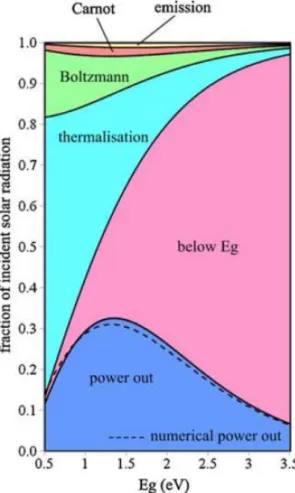
Figure 1 shows the results of theoretical calculation of loss mechanisms in single
pn junction solar cells versus the band gap of the semiconductor. We distinguish between the losses associated with lower energy photons, the thermalization losses associated with higher energy photons, in addition to other loss mechanisms. In the absence of such losses, the theoretical efficiency of photovoltaic cells may reach 80 to 90%. The figure shows that for a pn junction involving one single semiconductor, the theoretical conversion efficiency varies with the bandgap energy and reaches an optimum at about 30% for bandgap values in the range 1.2-1.5 eV. This is because the maximum photovoltage is proportional to the bandgap of the semiconductor, VCOmax = Eg / q (in fact, only 2/3 of this value can be reached at the best), while its
generated photocurrent decreases because all the photons of energy below the bandgap are not collected. Such opposite behaviors result in the presence of an optimum of efficiency.
Figure 1. Theoretical analysis of the loss mechanisms in a photovoltaic cell based on the bandgap. The blue area corresponds to the theoretical efficiency of a single junction cell under illumination AM1.5 (Hirst et al, 2011).
4
2.2- Present Photovoltaic technologies
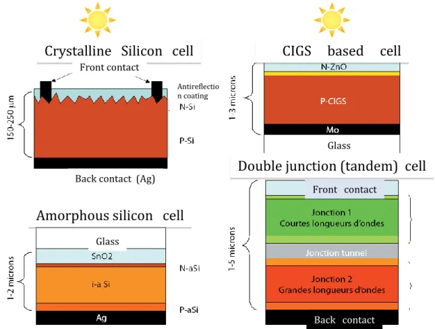
Figure 2 depicts the cell structures of the most used devices. Figure 2a is the structure using crystalline or multicrystalline silicon wafers, which represents about 90% of the market today. It is a typical N-P homojunction where conventionally, the N region is a phosphorus-doped silicon and the P region is a boron doped silicon substrate. Figure 2b concerns thin-film amorphous silicon (about 5% of the market). This is also a kind of homojunction where the intrinsic absorbing amorphous layer is sandwished in between the n and p type regions. Figure 2c displays the cell structure based on cadmium telluride (CdTe) whose market share increased from 1% in 2005 to nearly 8% in 2014. This is a heterojunction cell as the n- and p-type semiconductor materials are different, namely here CdS and CdTe resoectiveley. Finally, figure 2d gives the scheme of a CIGS (copper- indium- gallium diselenide) cell which cover approximately 1% of the market, still under strong development at labs and industry levels.
Figure 2. Schematic representation of the different current photovoltaic technologies: A) Conventional cell based on mono or multicrystalline silicon wafers. The pn junction is completed by a front electrical contact for collecting photogenerated electrons (in the case of a silver grid), and a back contact usually consisting of aluminium and deposited on the entire surface (screen printing process). The latter can collect the photogenerated holes. A texturing of the surface and the setting of an antireflection coating makes it possible to limit the optical losses by reflection. B) thin film cell based on amorphous silicon ; the front contact is transparent conductive tin oxide layer, while the back contact is a silver layer. C) thin film cell based on cadmium telluride (CdTe). The pn junction is made with cadmium sulfide (CdS). Contacts are tin oxide on one side and carbon on the other one. D) Cell based on thin-film copper indium and gallium diselenide (CIGS). The pn junction is made with CdS. The front contact is made of zinc oxide while the back contact is molybdenum.
Crystalline Silicon cell
CIGS based cell
Amorphous silicon cell
Double junction (tandem) cell
Front contact
Antireflectio n coating
Back contact (Ag)
Glass
Glass
Back contact
5 Figure 3 shows the evolution of record efficiencies for solar cells employing the different technologies10. The data concerns mature technologies such as those
involving crystalline silicon, thin films technologies based CIS, CdTe, or amorphous Si, single-junction GaAs, III-V multijunction compounds, as well as emerging technologies like in the case of organic or hybrid structures. One can notice that the record conversion efficiency reaches more than 46% for the multijunction based on GaAs, and it is lying between 22,1 and 25,6% for single junction cells (crystalline Si, CIS, CdTe), while it is between 13 to 21% for recently developed solar cells. Figure 3 plots also efficiencies data for cells made using nanostructures such as the dye sensitized cells (DSSC) and interpenetrating network organic cells (ORSC) or using nanomaterials such as the PbS quantum dots cells (QDSC). Much more recently, hybrid organic-inorganic cells like those based on perovskite materials have emerged and exhibit a very high potential with a record efficiency approaching 21% on small area.
One important message from Figure 3 is that a strong research and a smart engineering is necessary over years to reach a maturity for any technology.
The second message is that, besides the multijunction cells, none of the technologies based on a single junction have passed the Schockley-Queisser limit as the limiting losses are still present.
Figure 3. Evolution of record efficiencies obtained for the different photovoltaic technologies (Source NREL, http://www.nrel.gov/ncpv/images/efficiency_chart.jpg).
3- Nanomaterials for photovoltaics
To overcome the limitations mentioned in figure 1, innovation on material and device structure has become the cutting-edge of the current research. The focus is mainly on the improvement of the photon absorption and photon-carrier collection
6 efficiencies. Nanochemistry and nanomatériaux, provide numerous opportunities for a new generation of photovoltaics with high solar energy conversion efficiencies at low fabrication cost, provided it is possible to engineer the material properties through its chemical composition but also by tailoring the size and the shape. Here, we will examples of Quantum-confined nanomaterials and polymer–inorganic nanocomposites that can be tailored to harvest sun light over a broad range of the Spectrum. We will also review how plasmonic structures offer effective ways to reduce the thickness of light-absorbing layers. Finally, we will mention some concepts such as multiple exciton generation, photon down-conversion, and photon up-conversion realized in nanostructures that have significant interest for harvesting underutilized ultraviolet and currently unutilized infrared photons.
3.1- Quantum-confinement effects for photovoltaic 3.1.1- Principle
The nanostructures are characterized by novel and interesting properties that may be seriously different from those of the bulk material. At the nanoscale, the energies which are characteristics of the electronic levels, their interactions with photons, as well as the vibration modes of the atoms are strongly modified compared to their values in the bulk structure. This structuring at the nanoscale will thus open new opportunities in the photovoltaic conversion process. Lower is the size of these nano-objects compared to the bulk material, greater will be the gap between their physical properties and those at conventional shape. In particular, reducing the size of crystalline semiconductors to the nanoscale leads to remarquable effects such as the quantum confinement. At nanometric scales, the electrons behave more like waves than particles, and thus as phenomena that cannot be localized without affecting strongly the reachable energy levels (Heisenberg uncertainty principle). Based on the confinement direction, a quantum-confined structure will be classified into three categories as quantum well, quantum wire and quantum dots or nanocrystals. As more number of the dimension is confined, more discrete energy levels can be found, in other words, carrier movement is strongly confined in a given dimension. The quantum states densities and the energy dispersions versus the wave vector (k = 2π/λ) for the above-mentioned cases are shown in Figure 4. In the quantum dots for example, the energy does not vary linearly anymore. It is this feature that makes quantum dots of great interest to a number of advanced concepts and to the fabrication of a new branch of photovoltaics devices. These quantum dots can also be, in many ways, considered as "artificial atoms". The quantum dots as well as nanolayers or nanowires are often embedded in a material in which the electron wave functions do not overlap significantly. In the case of semiconductor nanocrystals such as silicon, germanium or lead sulphide, the host material is generally an insulating matrix allowing the transfer of electrons from one nanostructure to another by the tunnel effect.
7
Figure 4. Density of electron states of a semiconductor as a function of its dimension. The optical absorption spectrum is roughly proportional to the density of states.
Figures 4 b to d show that the reduction of the semiconductor crystal size to the nanoscale induces the discretization of the energy. The singular feature is that the width of the band gap Eg can be tuned versus the size of the nanowire or nanodot for
instance. This property can be exploited to absorb and convert more photons and / or generate more carriers with respect to the bulk material. The materials can be structured in the form of nanotubes, nanowires, quantum wells or quantum dots. In the case of spherical nanoparticles (nanodots) with a radius R, the energy bandgap is given by the relationship:
ERyd is the binding energy of excitons while me, mh are the effective masses of
electrons and holes, and h is Planck's constant. The second term takes into account the electrostatic interactions between the electron and the hole.
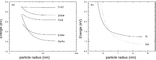
Figure 5 shows the variation of the optical gap as a function of the size of the nanoparticle for various semiconductors.
8 particle radius (nm) particle radius (nm)
Figure 5. Theoretical evolution of the optical bandgap of various types of spherical nanocrystals, according to their size and the nature of the material.
It can be seen that the quantum effect can increase significantly the value of the gap by several eV. Thus using the same material but varying its size, it becomes possible to tune the energy bandgap at a desired value. Figure 5b shows the results obtained in the case of silicon nanoparticles, which is the subject of numerous investigations as we will see below. The energy bandgap can be changed from 3 eV to 1.3 eV for Si-QDs of 1.2nm to 5nm respectively. Thus, one can say that the use of quantum size effects generates the possibility of engineering the bandgap of conventional semiconductors to a large extend, which is possible only by changing the chemical composition by introducing massive amount of impurities in a bulk material.
Figure 6 illustrates the dramatic effect of changing the bandgap in the case of CdTe nanoparticles, on the optical abosrption. The effect of particle size is clearly illustrated in the optical absorbance spectra (left) that show a blue shift (increase of the optical energy bandgap) when decreasing the particles size. The photograph at the right shows vials containing colloidal suspensions of CdTe QDs of different sizes under UV excitation. E n e rg ie (e V ) Rayon du la particule (nm) E n e rg ie (e V ) Rayon du la particule (nm)
9
Figure 6. (Left) Absorption spectra of colloidal suspensions of CdTe nanocrystal (NC) quantum dots of different sizes. (Right) Photograph of vials containing colloidal suspensions of CdTe QDs of different sizes under UV excitation. Reprinted with permission from Ref. [Groeneveld, E.: Synthesis and optical spectroscopy of (hetero)-nanocrystals. Ph.D. Thesis, Utrecht University, Utrecht (2012)
Another interesting consequence of the quantum confinement effect is the modification of the electron affinity of the semiconductor11, which may result in a
change of the energy diagrams. Figure 7 shows the example of the effect of quantum confinement in the case of CdSe nanoparticles on the photogenerated electron injection into the titanium oxide conduction band (Kongkanand et al., 2008).
Figure 7. Schematic representation of changes in the energy diagram of CdSe nanoparticles in contact with the titanium oxide (ref. 11). In Y axis is represented the energy with the conduction band and valence positions for the titanium oxide and for the CdSe particles according to their size. The abscissa axis represents the distance. The effect of the size of the CdSe particle is represented by different graphs on the x-axis for convenience.
In the following are reported few examples of solar cells illustrating whow the quantum-confinement effect is exploited.
3.1.2- Solar cells based on PbS or PbSe nanoparticles
The high absorption cross-section of colloidal nanocrystals or CQDs at tunable wavelengths makes them attractive for thin film solar cells, since this characteristic allows for optimal harvesting of the solar spectrum, thereby opening a promising route to high efficiency12,13 . Moreover, just like for QD-LEDs, solution processability
is a great asset, offering the prospect of low fabrication costs and easy upscaling. The exciton dissociation in QDs is also relatively easy and can be boosted by using heteronanocrystals architectures. These properties have led to the utilization of CQDs in a variety of different solar cell concepts14,15 .
11 Kongkanand A., Tvrdy K., Takechi K., Kuno M., Kamat P.V. (2008). J. Am. Chem. Soc. 130, 4007.
12 Konstantatos, G., Sargent, E.H.: Colloidal quantum dot optoelectronics and photovoltaics. Cambridge
University Press, Cambridge (2013),
13 Nozik, A.J., Conibeer, G., Beard, M.C.: Advanced concepts in photovoltaics. Royal Society of Chemistry,
Oxford (2014).
14 Lunt, R.R., Osedach, T.P., Brown, P.R., Rowehl, J.A., Bulovic, V.: Practical roadmap and limits to
10 As an example, bulk PbSe semiconductor has a low band gap of 0.27 eV which is obviuously not suitable for efficient photovoltaic conversion of solar energy. In contrast, the quantum size effect is potentially interesting to be able to increase the bandgap of a layer composed of PbSe nanoparticles (PbSe-NP). Similarly, bulk PbS with a gap of 0.37 eV is a good candidate for these studies16.
Synthesis of a PbS film composed of monodisperse nanoparticles (3 to 5 nm in diameter) can be performed by self-assembly of nanoparticle solution. The overlapping of the wave functions of the particles decreases the quantum confinement effect and therefore they stay spatially separated. In contrast, the transfer of electrons (and holes) from one particle to the other must remain possible and fast enough to avoid introducing series resistances which are detrimental to a high conversion efficiency. This question is central for the use of nanoparticles based films as there is indeed a conflict between quantum confinement effect and electron mobility. This highlights the interest for structures in which the confinement is possible in one or two directions only, preserving a direction for the efficient transfer of electrons. The transfer can be done by tunneling if the particles medium is insulating or by conduction if the particles medium is conducting. The results obtained with cells using PbS films have reached conversion efficiencies as high as 4% which is particularly encouraging (Figure 8). The performances are mostly due to low charge carrier mobility through the CQD-film and contact losses. Also, there is a demand for proper band alignment at electrodes for efficient charge extraction at minimal cost to voltage.
Figure 8. Photovoltaic properties of PbSe-NP based cells with bandgap (particle size) of 1,1 eV (4,3 nm) et 1,3 eV (3,5 nm). The conversion efficiency is of about 4%. (Ref. 16).
Recently, self-assembled monolayers (SAMs) were be used to modify interface energy levels locally. This was done through a process that secured anchoring of aromatic SAMs, aided by deposition of the SAMs in a water-free deposition environment17. The energy alignment at the rectifying interface was tailored by tuning
the robust SAM (R-SAM) for optimal alignment relative to the CQDs
15 Kramer, I.J., Sargent, E.H.: Colloidal quantum dot photovoltaics: a path forward. ACS Nano 5, 8506–8514
(2011)
16 Szandrei et al., 2010
17Gi-Hwan Kim, F. Pelayo García de Arquer Yung Jin Yoon, Xinzheng Lan, Mengxia Liu, Oleksandr Voznyy, Zhenyu Yang, Fengjia Fan, Alexander H. Ip, Pongsakorn Kanjanaboos, Sjoerd Hoogland, Jin Young Kim, and Edward H. Sargent, Nano Lett., 2015, 15 (11), pp 7691–7696
11 confined electron energy levels. Figure 9a gives the schema of the PbS CQDs based cell using the SAMs structure. Figure 9b displays the illuminated J-V characteristics of the CQDs/SAM cell exhibiing a record power conversion efficiency (PCE) of 10.7% (17).
Figure 9: (a) schema of the PbS CQDs based cell using the SAMs structure; (b) J-V characteristics under illumination of the CQDs/SAM cell (ref. 17).
3.1.3- Solar cells based on silicon nanoparticles
One of the most interesting examples of quantum effects using silicon nanostructures (wells, wires, dots) is to produce multijunctions solar cells based solely on silicon (figure 10a). In the case of silicon nanocrystals, they are often embedded in a dielectric matrix obtained by several deposition techniques such as Plasma enhanced CVD, evaporation or sputtering. Figure 10b shows the example of a superlattice composed of a stack of sub-stochiometric SiOx and stochiometric SiO2
nanolayers. The control of the bandgap energy can be obtained by controlling the size of the silicon nanocrystals (figure 9c), which is governed by the tickness of the nanolayers. The nanoparticle size is the key parameter to adjust the absorption of the total thin layer. The conduction properties depend on the matrix wherein the Si-ncs are integrated (the barrier height between the particules controls the probability of charges transfer between them). Reducing the distance between the silicon nanocrystals leads to the formation of mini-bands which results in an effective energy bandgap larger than that of bulk silicon. This perspective generate the concept of « all silicon » tandem cell suggesting the possibility of a significant increase in the open circuit voltage (larger bandgap) in comparison to a single junction. Theoretically, a configuration like that of figure 9a is expected to deliver a quantum efficiency of about 29%18.
12
Figure 10. (a) scheme of a “QDs based silicon” tandem cell; (b) TEM of alternated layers of pure followed by silicon-rich oxide, nitride or carbide. Upon thermal annealing, silicon precipitates out of the silicon-rich phase as spherical quantum-dots of diameter nominally equal to the layer thicknesss (figure at right).(Ref. 18)
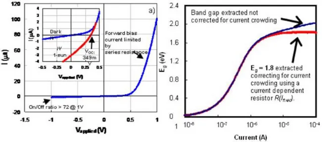
Fabrication of solar cells involving silicon nanoparticles is quite complicated and it is still under development. While the optical effects were already observed, the transport properties are very limiting. However, first demonstrators employing a single junction19 have been produced and an example is shown in Figure 11. An
open circuit voltage up to 350mV was obtained but the current is low. In such structures, the question of n-doped and p-doped nanoparticles was also introduced so as to allow the realization of pn or pin type cells.
Figure 11. First results from cells using quantum effects in silicon. The band gap of the top layer containg silicon nanoparticles is about 1.8 eV (Conibeer, Green et al, 2010).
19 Conibeer G., Green M., König D., Perez-Wurfl I., Huang S., Hao X., Di D., Shi L., Shrestha S., Puthen-Veetil B.,
SoY., Zhang B., Wan Z. (2010). Proceedings 25th European Photovoltaic Solar Energy Conference, Valencia,
13
3.2 Geometric-confinement effects for photovoltaics 3.2.1 - Principe
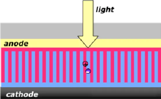
In the case of a conventional photovoltaic cell, the optical absorption depth usually has a thickness less than the active thickness for the separation and efficient collection of the electron-hole pairs. One alternative way to collect efficientyly the electron-hole pairs is to reduce the absorption volume into small domains of thicknesses lower that the carriers’ diffusion length. These domains should have thicknesses from a few nanometers to a few tens of nanometers. The concept was applied to nanostucture the space between n-type (collection of electrons) and p-type (collection of holes) regions. This design, far from that of a conventional photovoltaic cell, is called "interpenetrated junctions" or "bulk heterojunction" (Figure 12). It has in fact been introduced in early 90ths for the photoelectrochemical dye cells20, and later
applied to organic cells. It can be also extended to inorganic materials based on nanowires or nanorods.
Figure 12. Schematic of an ideal interpenetrating junctions structures composed of
donor and acceptor nanomaterials
3.2.2- Organic and hybrid nanostructured cells
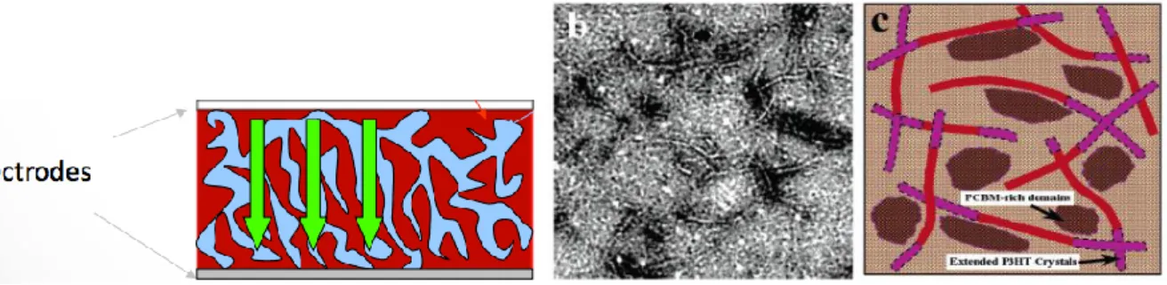
Figures 13a gives a schema of a bulk heterojunction (BHJ) structure consisting of a donor material (polymer) and an acceptor material (fullerene, polymer, inorganic) finely mixed to obtain an active layer morphology. It presents randomized domains whose characteristic dimensions are close to the exciton diffusion length (10 to 20 nm). This morphology, by providing sufficient donor-acceptor interfaces, enhances the probability of exciton dissociation. Figure 13b shows a microscope image of a bulk heterojunction composed of P3HT and PCBM, the most studied organic mix. Current high-efficiency polymer solar cells (PSCs)21 with efficiencies above 9.0% are
restricted to materials combinations that are based on limited donor polymers and only one specific fullerene acceptor, PC71BM. Furthermore, best-efficiency PSCs are
20 O’Regan B., Grätzel M. (1991). Nature 353 737.
21Liu, Y., Zhao, J., Li, Z., Mu, C., Ma, W., Hu, H., Jiang, K., Lin, H., Ade, H. and Yan, H., “Aggregation and morphology control enables multiple cases of high-efficiency polymer solar cells.” Nat. Commun., 5, 5293, (2014).
14 mostly based on relatively thin (100 nm) active layers. Thick-film PSCs generally exhibit lower fill factors and efficiencies compared to the best thin-film PSCs. Recently were repoted multiple cases of high-performance thick-film (300 nm) PSCs based on conventional PCBM and many non-PCBM fullerenes with efficiencies up to 10.8%22. The simple aggregation control and materials design rules allowed to
develop three new donor polymer, six fullerenes (including C60-based fullerenes), and over ten polymer:fullerene combinations, all of which yielded higher efficiency than previous state of art devices. A record certified efficiency of 11.7% was demonstrated (ref.22).
Figure 13. Structure of the active layer of an organic solar cell. (29a): Junction
consists of an interpenetrating mixture of donor and acceptor materials (P3HT and PCBM in the figure). (11b) a schema of figure 13a for illustration purpose.
One of the major limitation of the interpenetrating network structure is it does not fulley support the transport of charges to the electrodes. The carriers must indeed make their way through the donor and acceptor materials to the electrodes. To improve the carriers transport, while maintaining optimal exciton separation, controlled nanostructure junction structure is necessary. Among the options, the donor material can be a vertical nanowires embedded in an acceptor material matrix. The nanowires should have a diameter in the order of the exciton diffusion length, typically 10 to 20 nm, and a length compatible with the carriers diffusion length to the electrodes (of the order of 100 nm). The nanowires are used to generate percolation paths to the electrodes. However, the fabrication of such structures is difficult and it is still a subject of intense research. It can be noted that the transport properties in these disordered systems can be improved by controlling the morphology of the mixture (domain size and degree of crystallinity). For instance, some groups developed methods of structuring the P3HT as fibrils that are obtained in solution prior to the spinning step23. In these fibrils, the polymer chains are highly ordered and
conversion efficiencies around 4-5% were reported while overcoming the conventional post-deposition annealing. Further work has concerned the replacement of the fullerene molecules by carbon nanotubes in order to facilitate the organization of the layers and improve the electron transport properties.
Another nanostructured type of cell is the hybrid dye solar cells composed of TiO2
nanoparticles, decorated with dye molecules and embedded in a iodine based electrolyte. The transport properties in the porous oxide matrix are also an issue that
22 Jingbo Zhao, Yunke Li, Guofang Yang, Kui Jiang, Haoran Lin, Harald Ade, Wei Ma & He Yan, Nature Energy 1,
Article number: 15027 (2016)
23 Monestier F., Simon J.-J., Torchio Ph., Escoubas L., Flory F., Bailly S., De Bettignies R., Guillerez S.,
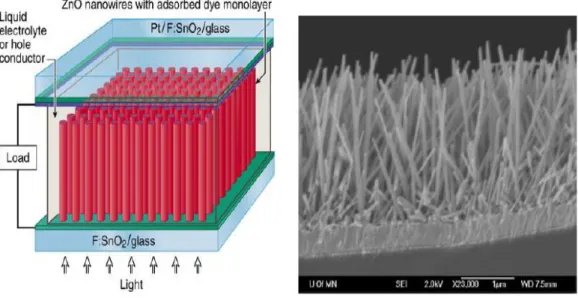
15 should be improved. There may be mentioned in particular the embodiment of monocrystalline ZnO porous matrices obtained by the electrochemical deposition in the presence of structuring agents. In this case, there is no barrier at the grain boundaries as in the case of conventional structures obtained by sintering. Figure 14a shows a typical example of an ETA cell24. It uses a network of nanocolumns as
electron carriers ("electron highways'). Figure 14b shows a network of ZnO nanocolumns as produced by electrolysis. As an example of application, Optimized ZnO/CdSe/CuSCN solar cells exhibiting 3.2 % solar energy conversion efficiency were obtained by using 230 nm diameter ZnO NWs25.
Figure 14. left: typical scheme of an ETA cell; Right: array of nanowires of ZnO single crystal electrochemically deposited on a layer of TCO (SnO2) (ref. 25).
3.2.2- Nanostructured cells based on silicon or III-V compounds
The use of nanostructures tends to extend also to conventional materials commonly employed in planar configurations. A trivial example concerns the cells based on nanostructured silicon. The first approach is to use arrays of SiNWs to improve light absorption in Si in both different ways26,27: while random multiple
scattering in SiNW arrays enhances broadband light absorption, resonant optical phenomena such as Mie scattering at individual SiNWs constitute the optical response of the entire absorber, i.e. cause an overall wavelength-, angle- or polarization- selective photonic absorption enhancement28. The second approach is
targeting to fabricate silicon nanowires based solar cells. In this case, the orthogonal
24 I. Kaiser, K. Ernst, Ch.-H. Fischer, R. KoK nenkamp, C. Rost, I. Sieber, M.Ch. Lux-Steiner ; Solar Energy
Materials & Solar Cells 67 (2001) pp.89-96
25 C. Levy-Clement, J. Elias, Journal of Chemistry Physics and Physical Chemistry, V.14(10), 2013
pp. 2321–2330
26 Tsakalakos, L.; Balch, J.; Fronheiser, J.; Korevaar, B. A.; Sulima, O.; Rand, J. Silicon Nanowire Solar Cells.
Appl. Phys. Lett. 2007, 91, 233117
27 Garnett, E. C.; Yang, P. Light Trapping in Silicon Nanowire Solar Cells. Nano Lett. 2010, 10, 1082–1087. 28 Brönstrup, G.; Garwe, F.; Csáki, A.; Fritzsche, W.; Steinbrück, A.; Christiansen, S. Statistical Model on the
16 direction between the charge-carrier collection path and incident light enables the use of low-quality silicon in the production of solar cells. The material cost and amenability to eventual large scale fabrication determine the viability of novel concepts in solar cell design in addition to efficiency. The SiNWs can be grown on solids using the thoroughly studied vapor-liquid-solid (VLS) process or modifications of which, e.g. the vapor-solid-solid (VSS) growth. These processes are relying on catalytic growth of Si from metal-Si eutectics under continuous supply of the silicon growth species from the gas phase in chemical-vapor-deposition (CVD) reactors29.
Here, the size and arrangement of grown SiNW is dependent on the previous deposition of a metal catalyst mask on top of the solid substrate. However, even though these so called bottom-up processes produce SiNW of uniform shape and good crystalline structure, their electrical quality was found to be strongly influenced by the incorporation of metal catalyst atoms that cause inter band trap states in silicon30.
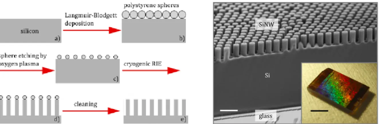
Another method of fabricating hexagonally aligned arrays of silicon nanostructures is the cryogenic RIE in combination with polystyrene nanosphere (PSNS) lithography31. The process flow is shown in Figure 15. Nanowires and
nanorods can be fabricated using this method.
It is also possible to fabricate symmetric or antisymmetric NWs using top-down lithography with a dry etching process and silicon oxyde as a mask32. Figure 16a
illustrates the asymmetric silicon nanowire (SiNW) solar cell structure. A maximum short circuit current density of 27.5 mA/cm2 and an efficiency of 7.53% were realized
without anti-reflection coating. Changing the silicon nanowire (SiNW) structure from conventional symmetric to asymmetric nature improves the efficiency due to increased short circuit current density. This is well demonstrated in figure 14b. The proposed asymmetric structure has great potential to effectively improve the efficiency of the SiNW solar cells.
29 Wagner, R. S.; Ellis, W. C. Vapor-Liquid-Solid Mechanism of Single Crystal Growth. Appl. Phys. Lett. 1964, 4,
89.
30 Hannon, J. B.; Kodambaka, S.; Ross, F. M.; Tromp, R. M. The Influence of the Surface Migration of Gold on the
Growth of Silicon Nanowires. Nature 2006, 440, 69–71.
31 Cheung, C. L.; Nikolic, R. J.; Reinhardt, C. E.; Wang, T. F. Fabrication of Nanopillars by Nanosphere
Lithography. Nanotechnology 2006, 17, 1339–1343.
32 Ko, M.-D. et al. High efficiency silicon solar cell based on asymmetric nanowire. Sci. Rep. 5, 11646; doi:
17
Figure 15 : Process steps for the fabrication of SiNWs by PSNS lithography and RIE : On a clean silicon surface a PSNS colloidal crystal was deposited via a Langmuir Blodgett (LB) through (a, b). Subsequently, the sample was transferred to the RIE reactor and the PSNS were reduced to the desired size via oxidation in an O2 plasma
(c). With the PSNS of remaining size masking the surface, the poly-Si sample were exposed to a cryogenic RIE plasma to selectively etch the non-covered surface area (d. Cleaning was performed with a dip in an ultra-sonic bath to remove the spheres and rinsing in ethyl acetate/isopropanol to dissolve the thermal coupling oil (Fomblin) for the cryogenic RIE process. The processing was finalized by a thermal annealing in O2 (500°C / 30
min) and a dip in hydrofluoric acid to remove remaining surface damage and roughness from the as-etched structures (e). SEM image of SiNWs produced by the PSNS lithography method and RIE on silicon on glass. With the courtesy of Y. Schmitt.
Beyond photovoltaics, the individual and interconnected silicon nanowire elements can serve as robust power sources to drive functional nanoelectronic sensors and logic gates. These coaxial silicon nanowires provide a new nanoscale test bed for studies of photoinduced energy/charge transport and artificial photosynthesis, and might find general usage as elements for powering ultralow-power electronics and diverse nanosystems.
Figure 16: (a) Schematic illustration of the asymmetric silicon nanowire (SiNW) solar cell consisting of an array of radial p-n junction asymmetric SiNWs, back surface field (BSF) layer, Al back reflector and Ag top electrode. ; (b) The distribution of the efficiency of four types of SiNW solar cells. DB is the core
diameter at the bottom of the nanowire. Each distribution comes from the J-V characteristics of the solar cells fabricated with identical design and process parameters.
Si
glass a)
18 Recently, highly efficient hybrid solar cells based on silicon nanowires (SiNWs) and poly(3,4-ethylenedioxythiophene):poly(styrenesulfonate) (PEDOT:PSS) using transfer-imprinted metal mesh frnt electrodes were reported33. Compared with hybrid
cells formed using indium tin oxide (ITO) electrodes, they find an increase in power conversion efficiency from 5.95% to 13.2%, which is attributed to improvements in both the electrical and optical properties of the Au mesh electrode. The proposed fabrication strategy for metal mesh electrode is suitable for the large-scale fabrication of flexible transparent electrodes, paving the way towards low-cost, high-efficiency, flexible solar cells.
This organic-inorganic approach was also applied to the III-V GaAs-based semiconductor. For instance, hybrid solar cells based on poly(3-hexylthiophene)-coated GaAs nanopillars grown on a patterned GaAs substrate using selective-area metal organic chemical vapor déposition were reported.34
3.3- Optical Management based on nanostructures 3.3.1 Plasmonics for photovoltaics
The study of plasmonics in solar cells has developed over the past ten years. The issue was to increase light absorption in materials used for solar cells. Coupling of light energy in the form of plasmons is thus of high interest in thin-film solar cells, when the price of the material can be a hindrance to the development of the technology.
In physics, a plasmon is a quantum of plasma oscillation arisen from the free electron "gas" in conducting material35. There are three types of plasmons, bulk plasmon (located in a bulk conducting material), surface plasmon (located at planar
metal-dielectric interfaces) and localized surface plasmon (highly confined on a small surface, e.g., on the surface of a nanoparticle). In an infinite solid (e.g., metal), the bulk plasmons are longitudinal waves36. According to the Drude model37, if the
frequency of an incident electromagnetic wave is higher than bulk plasmon frequency, the metal becomes transparent for this wave. The bulk plasmon frequencies of most metals are in the ultraviolet region, associating energies within 5-15 eV. But for some metals, e.g., noble metals (copper, silver and gold), they have filled d-shells. These d-electron bands have lower energies than the Fermi level of the conduction band and thus allowing new narrow transitions close to or in visible region38. Due to the fact that light waves are transverse, the wave vector mismatch
makes the bulk plasmons incapable to be excited from direct irradiation, thus strongly limiting their utilization in the photovoltaic domain. Surface plasmons are plasmons at the metal-dielectric interfaces and tightly bound to the interfaces. Since their wave-vector is larger than light waves, the surface plasmon cannot be directly excited by illumination. Instead, the surface plasmon wave can be generated under special
33Park, K.-T. et al. 13.2% efficiency Si nanowire/PEDOT:PSS hybrid solar cell using a transfer-imprinted Au mesh
electrode. Sci. Rep. 5, 12093; doi: 10.1038/srep12093 (2015).
34 Giacomo Mariani et al., Hybrid conjugated polymer solar cells using patterned GaAs nanopillars, Appl. Phys.
Lett. 97, 013107 (2010)
35 D. Pines, "Collective energy losses in solids," Rev. Mod. Phys. 28, 184–199 (1956)
36 R. A. Ferrell, "Predicted Radiation of Plasma Oscillations in Metal Films," Phys. Rev. 111, 1214 (1958). 37 L. Tonks and I. Langmuir, "Oscillations in ionized gases," Phys. Rev. 33, 195 (1929)
19 geometries (Kretschmann coupler39, gratings40). The surface plasmon propagates
along the dielectric/metal interface and it has a highly concentrated electric field near the interface. This electric field exponentially decays away from the surface. The decay rate is much higher in metal than in dielectric. Localized surface plasmons excited in metallic nanoparticles are non-propagating plasmon excitations. Since the size of a metallic nanoparticle is on the same scale of the penetration depth of electromagnetic waves in metals (e.g., 20 ~ 30 nm for Ag and Au), the external field can penetrate the whole particles and shift the conduction electrons with respect to the rigid ion lattice. Thus, the charges are separated and this charge separation results in a restoring force and then an oscillation. The oscillation frequency is mainly related to effective electron mass, charge density and geometry of the particle, as well as the properties of the surrounding medium. The amplitude of the induced electromagnetic field is much stronger than exciting fields (over 10 times). The properties of localized surface plasmons in noble metallic nanoparticles can be tuned by the composition, size, shape and their environment414243.
A comprehensive review on the applications of plasmon effect to solar cells has been published by Atwater and Polman44 45. More specific work concerns the wafer
or thin film silicon solar cell types with a strong increase of the optical absorption for wavelengths close to the gap46. In organic solar cell, an improvement of the
conversion efficiency was obtained with gold nanoparticles in the active layer and silver electrodes including a diffraction grating4748.
For solar cells, particularly in thin film form, the coupling of surface plasmons can therefore allow a trapping, at the interface between the semiconductor material and the back electrode, of a part of the radiation that is not or little absorbed within the semiconductor, for example, the radiation part which is close to the gap of the semiconductor. To do so the back electrode of the cell is periodically structured in the form of mono- or two-dimensional grating. This grating allows both to excite surface plasmon in a specific spectral range but it can also play the role of a rear mirror and have an influence on the coupling of Fabry-Perot type modes in a wider spectral range, in the overall structure of the solar cell49 50 (fig. 17).
39 E. Kretschmann, "The Determination of the Optical Constants of Metals by Excitation of Surface Plasmons,"
Zeitschrift für Phys. 241, 313–324 (1971)
40 E. Devaux, T. W. Ebbesen, J.-C. Weber, and “ A. D., "Launching and decoupling surface plasmons via
micro-gratings," Appl. Phys. Lett. 83, 4936 (2003).
41 E. Stefan Kooij and B. Poelsema, "Shape and size effects in the optical properties of metallic nanorods.," Phys.
Chem. Chem. Phys. 8, 3349–57 (2006).
42 C. Noguez, "Surface Plasmons on Metal Nanoparticles: The Influence of Shape and Physical Environment," J.
Phys. Chem. C 111, 3806–3819 (2007).
43 K.-S. Lee and M. A. El-Sayed, "Dependence of the enhanced optical scattering efficiency relative to that of
absorption for gold metal nanorods on aspect ratio, size, end-cap shape, and medium refractive index.," J. Phys. Chem. B 109, 20331–8 (2005).
44 H. Atwater, A. Polman, « Plasmonic for improved photovoltaic devices », Nature Materials 9 (3), 205-213 (2010)
45 K. Catchpole, A. Polman, « Plasmonic solar cells », Optics Express 16 (26), 21793 – 21800 (2008)
46 S ; Pillai, K. Catchpole, T. Trupke et al., « Surface plasmon enhanced solar cells », Journal of Applied physics
101 (9), 093105 (2007)
47 X. Li, W. Choy, L. Huo et al., « Dual plasmonic nanostructures for high performance inverted organic solar
cells », Adv. Mat. 24 (22), 3046-3052 (2012)
48 D. Duche et al., “Improving light absorption in organic solar cells by plasmonic contribution”, Solar Energy
Materials & Solar Cells 93, 1377–1382 (2009)
49 B. Behaghel et al., « Absorption enhancement through Fabry-Perot resonant modes in a 430nm thick
InGaAs/GaAsP multiple quantum wells solar cell », APL 106, 081107 (2015)
50 I. Massiot, N. Vandamme et al., « Metal Nanogrid for Broadband Multiresonant Light-Harvesting in Ultrathin
20
Figure 17: Reproduced from ref 34 (I. Massiot et al.) Measured (a) and calculated (b) total absorption spectra at normal incidence of the SiNx (Au)/GaAs/Au structure. Inset of (a) SEM image of the 2D gold nanogrid. Inset of (b) : schematic of the structure modeled with a rectangular surface profile.
The excitation of these resonance modes in surface or in volume allows exalting the light absorption within the semiconductor material, and thus increases the photocurrent.
If we now look at the localized plasmons, the principle of increasing photon absorption is totally different. Indeed, the incident light radiation is partially scattered by the metal nanoparticles and partly absorbed in the metal. In the latter case, light energy is lost through thermalization and does not contribute to increase absorption in the semiconductor material. The light radiation which is scattered by metal nanoparticles is usually more efficiently absorbed within the semiconductor material just because the optical path in the material is increased51. Depending on the density
of metal nanoparticles and thus the distance between the nanoparticles, an electromagnetic coupling may occur between the latter. Under certain conditions of size and density of the metal nanoparticles, this coupling can lead to an exalted light scattering, enabling to further increase the absorption of radiation in the semiconductor material. The shape of the metal nanoparticles, which may be spherical, prismatic, cylindrical or in tetrapod forms, has an influence on the excitation wavelength of the plasmon52 53 54 (fig. 18). Compared to a sphere, in
nanoparticles with sharper curvatures area along the polarization direction of light there is weaker restoring strength leading to a lower plasmon resonance frequency (redshift) 55.
51 D. Derkacs, S. H. Lim, P. Matheu et al., « Improved performance of amorphous silicon solar cells via scattering
from surface plasmon polaritons in nearby mettalic nanoparticles », APL 89 (9), 093103 (2006)
52 K. L. Kelly, E. Coronado, L. L. Zhao, and G. C. Schatz, "The Optical Properties of Metal Nanoparticles: The
Influence of Size, Shape, and Dielectric Environment," J. Phys. Chem. B 107, 668–677 (2003).
53 X. Zhang, E. M. Hicks, J. Zhao, G. C. Schatz, and R. P. Van Duyne, "Electrochemical Tuning of Silver
Nanoparticles Fabricated by Nanosphere Lithography," Nano Lett. 5, 1503–1507 (2005).
54 Z. Cao, Z. Chen, L. Escoubas, « Optical, structural and electrical properties of PEDOT :PSS thin films doped
with silver nanoprisms », Opt. Mat. Express 4 (12), 2525-2534 (2014)
55 P. K. Jain, "Plasmons in assembled metal nanostructures: radiative and nonradiative properties, near-field
coupling and its universal scaling behavior," Dissertation presented at The Academic Faculty of Georgia Institute of Technology (2008)
21
Figure 18 : Reproduced from ref 38 (Z. Cao et al.) Normalized solution UV-Vis spectra of Ag nanoprisms synthesized from different volumes of a seed solution: black - seeds only; red - 2 mL; blue - 1mL; dark cyan - 650 μL; pink – 500 μL. The use of different amount of seed solution leads to different batches of Ag nanoprisms of different edge-length/thickness aspect ratios. Inset: TEM image of flat-lying Ag nanoprisms which show an in-plane localized surface plasmon resonance band at l=560 nm.
3.3.2- Up / Down photon Conversion for photovoltaics
The main limitations of photovoltaic efficiency of a single junction solar cell are the thermalization of the high energy photons and the non absorption of photons having energies lower than the bandgap energy of the absorbing semiconductor. Thus, potentially, changes in the incident solar spectrum may allow a standard cell to achieve a very high efficiency, provided to convert the wavelength of the incident photons to that corresponding to the bandgap of the semiconductor. The envisaged concepts to overcome partially these limitations are illustrated in Figure 19.
Basically, the challenge is to fabricate a component that absorbs a photon of energy at least twice the energy gap of the used semiconductor and to generate two incident photons in the cell (downconverter or DC (Figure 19.a), sometimes referred to as quantum-cutting). Down-shifting or DS (Figure 19.b) is also an optical process similar to DC with the exception that one high-energy photon (blue) is absorbed and converted into a single lower-energy photon (red). In this case, the only effect is to ‘shift’ high-energy photons into a more efficient region of the solar cell’s spectral response which is typically at a lower energy. The other challenge for up-conversion or UC (Figure 19.c) is to find a component that absorbs at least two photons having less energy than the bandgap and that emit a photon of energy above the bandgap. For all processes, the resulting photons have energy just above the bandgap of the active semiconductor, which corresponds to the most efficient energy absorption.
From a purely theoretical side, a maximum efficiency of 38.6% is achievable for a down-converter with bandgap of 2.2 eV located on the front surface of a solar cell with bandgap of 1.1 eV (corresponds to that of silicon). On the other hand, detailed balance calculations show that the efficiency of silicon solar cells can increase to 40.2% when coupled to an UC layer. From the processing point of view, no modification of the active part of the cell is necessary in contrast to the case for
22 multijunction cells mentioned above. However, few experimental developments exist involving nanomaterials.
Figure 19. Principle of spectrum modification by (a) down-convesion, (b) down-shifting and (c) up- conversion to increase the performance of a solar cell.
Different materials have been investigated in the literature for down-shifting layers such as organic dyes, quantum dots and rare earth ions. Organic dyes exhibit the highest optical conversion efficiency but lack stability and have an overlap between the absorption and emission peaks. Rare earth doped glass fluorescent materials have lower efficiencies but higher stability and larger stokes shift. Quantum dots have the distinct advantage of a tunable absorption profile by changing their size. Thus, the use of a layer containing CdS QDs (emitting at 610 nm) covering the surface of a polycrystalline silicon cell56 showed an ~ 28% increase in the circuit current and a
relative enhancement of the yield ~ 6%in the case of a diffuse AM1.5 radiation. Other works have investigated the effects of the down shifting layers and to demonstrate a gain in conversion efficency. Svrcek et al.57 have demonstrated a gain in the UV
region of the spectral response of a conventional P-N junction silicon solar cell using Si nanoparticles dispersed in a sol-gel solution. Pi58 et al. have also been able to
improve the absorption in the blue using a film rich in silicon nanoparticles deposited by spin coating on a crystalline silicon solar cell. The overall cell efficiency increased from 16.9 to 17.5%. More recently, silicon oxide layers containing silicon nanoparticles deposited by PECVD have been applied on back contact silicon solar cells59. An enhancement in the blue region of the internal quantum efficiency was
measured which has been translated in an improvement in efficiency for the best cell from 19.4 to 20.3%. Other approaches use oxides matrices (ZnO, SnOx, CeO2…) doped with rare earths such as Nd, Yb or Pr60. Thanks to their thickness of less than
56 Van Stark W.G.J.H. (2005). Appl. Phys. Lett. 87, 151117 57 Švrček V., Slaoui A., Muller J.-C. (2004). J. Appl. Phys. 95, 3158
58Pi, X.et al. Air-stable full-visible-spectrum emission from silicon nanocrystals synthesized by an all-gas-phase
plasma approach. Nanotechnology 19, 245603 (2008).
59 Delachat F., Slaoui A. (2009). Nanotechnology 20 , 415608; F. Sgrignuoli, P. Ingenhoven, G. Pucker, V.D.
Mihailetchi, E. Froner, Y. Jestin, E. Moser, G. Sànchez, L. Pavesi ; Solar Energy Materials & Solar Cells 132 (2015) 267–274
60 P M. Balestrieri, M. Gallart, M. Ziegler, P. Bazylewski, G. Ferblantier, G. Schmerber, G.S. Chang, P. Gilliot, D.
23 100nm and the appropriate refractive index, such layers are also playing the role of an antireflection coating for the solar cell. Though still very few breaktroughs are reported, the results for their use as DS converters are encouraging.
Concerning the up-conversion process, since the UC layers absorb photons that could have not be absorbed by the solar cell61, those layers are coupled to the back
surface of bifacial solar cells, and their presence cannot decrease the efficiency of the cell as in the case of poor choice of the down-shifting layers. Trivalent erbium, Er3+, is ideally suited for UC of near-infrared light due to its ladder of nearly equally
spaced energy levels that are multiples of the 4I15/2 to 4I13/2 transition. The Er3+ ion is
well suited for silicon solar cells as the absorption spectrum is centered at 1520 nm while the emission peaks occur at 980 nm, 880 nm and 650 nm. Another common choice for UC are coupled Er3+/Yb3+ ions, which are suitable for larger bandgap
devices such as CdTe or amorphous silicon solar cells since the absorption profile of Yb3+ is centered at 980 nm. Such elements are usually inserted in less than 100nm
thick oxide (ZnO, TiO2, ...) or fluroide (NaYF4) matrices62. One can mention the
results obtained with erbium and ytterbium doped NaYF4, which demonstrate a conversion efficiency of 17% of the infrared radiation at 1.57 micron to 1 a micron radiation63.
Note that the process of up-convertion is implementing several basic steps of absorption. Its effectiveness increases with the light concentration. One must therefore consider working in high concentration. Another possibility is the coupling of UC process with nanophotonics, especially plasmonic resonances modes since the increasing of the local field will enhance the probability of the UC process. Thus, application of plasmonic structure for up-conversion enhancement has been realized using Er3+ doped YF3 as up- converter layer64. In spite of the low thickness of films
(<100nm) and the low concentration of doping ions, up-conversion luminescence visible with naked eye has been obtained under 1540 nm wavelength excitation. Luminescence cartography showed that up-conversion enhancement up to a factor 5 has been obtained. Comparison between the structured layers and layers of the same thickness and the same Er3+ concentration shows that the enhancement factor of up-conversion luminescence can reach up to 35 by using plasmonic structures.
3.3.3- Multiple exciton generation Solar cells
The principle of multiple exciton generation (MEG) is to exploit the surplus energy of hot carriers to create one or more additional electron-hole pairs. A photon with very high energy will create a first high energy exciton, which can subsequentely decay
61 Strümpel C., McCann M., Beaucarne G., Arkhipov V., Slaoui A., Švrček V., Del Cañizo C. and Tobias I. (2007).
Solar Energy Materials and Solar Cells 91 (4) 238-249
62 Petersen J., Brimont C., Gallart M., Crégut O., Schmerber G., Gilliot P., Hönerlage B., Ulhaq-Bouillet C.,
Rehspringer J. L., Leuvrey C., Colis S., Slaoui A. and Dinia A. (2008). J. Appl. Phys. 104 113539
63 Ivanova S., Pellé F., Esteban R., Laroche M., Greffet J.J., Colin S., Pelouard J.L., Guillemoles J.F. (2008).
Proc. 23rd European Photovoltaic Solar Energy Conference, Valencia, ( 2008).
64 C. Andriamiadamanana A. Ferrier, L. Lombez, A-L. Joudrier, N. Naghavi, P. Ghenuche, N. Bardou, J-L.
Pelouard, S. Collin, F. Pelléand J-F. Guillemoles, Physics, Simulation, and Photonic Engineering of Photovoltaic Devices, Edited by Alexandre Freundlich, Jean-Francois F. Guillemoles, Proc. of SPIE Vol. 8256, 825608 (2012.
24 into as many excitons as allowed by energy conservation, by an impact ionization phenomenon. This is schematically illustrated in Figure 20 taken from the review done by A. Nozik65. This process could help to increase the theoretical maximum
efficiency for a single junction from 30% to about 40% or more depending on the threshold energy and on the processes considered66,67,68,69. Such phenomena have
been observed in the context of solar energy conversion in bot bulk and QD materials, and it is still debated whether the processes are more efficient in QD than in bulk materials70,71 .
This multiple exciton generation phenomenon was observed experimentally after excitation by a single photon of InAs, CdS, PbS or PbSe nanoparticles (NPs) with the generation of up to 8 excitons (ref. A. Nozik). More recently, investigations of MEG in close-packed Si QDs embedded in a silica matrix have yielded some interesting results. The first demonstration of MEG in Si utilized colloidal QDs with a diameter of 9.5 nm (Figure 21) and Eg= 1.2 eV, and reported hv (threshold)= 2.4 Eg and a quantum yield of 2.6 for a pump photon energy of 3.4 Eg (Figure 21)72.
Figure 20. Left : relaxation process of hot carriers in a conventional semiconductor. Excess photon energy is transferred as heat. Right: generation process of two excitons by absorption of a photon in a quantum dot (e.g. PbSe or PbS) thanks to the phenomenon of ionization by impact. The generation of a second exciton is faster than the conventional thermal transfer by interaction with phonons due to the quantization of energy levels. (ref.65).
By using photoluminescence quantum yield measurements and also subsequently ultrafast transient absorption spectroscopy, the step-like enhancement
65 Nozik A. J. (2008). Chemical Physics Letters 457 3.
66 R. Brendel, J. Werner, H. Queisser, Solar Energy Materials and Solar Cells 41/42 (1996) 419. 67 P. Landsberg, H. Nussbaumer, G. Willeke, J. Appl. Phys. 74 (1993) 1451;
68 W. Spirkl, H. Ries, Phys. Rev. B 52 (1995) 11319;
69 De Vos, Alexis, et Bart Desoete. « On the ideal performance of solar cells with larger-than-unity quantum
efficiency ». Solar energy materials and solar cells 51, no 3 (1998): 413-24]
70 Geiregat, Pieter, Christophe Delerue, Yolanda Justo, Michiel Aerts, Frank Spoor, Dries Van Thourhout, Laurens
D. A. Siebbeles, Guy Allan, Arjan J. Houtepen, et Zeger Hens. « A Phonon Scattering Bottleneck for Carrier Cooling in Lead Chalcogenide Nanocrystals ». ACS Nano 9, no 1 (27 janvier 2015): 778-88. doi:10.1021/nn5062723
71 Charles Smith and David Binks , Multiple Exciton Generation in Colloidal Nanocrystals, Nanomaterials 2014, 4,
19-45
72 M. C. Beard , K. P. Knutsen , P. Yu ,J. M. Luther ,Q. Song ,W. K. Metzger, R. J. Ellingson , and A. J. Nozik,
25 in the quantum yield of photo-generated charges that has been predicted for very high efficiency MEG has been reported73.
Figure 20: (left) a TEM image of a silicon nanocrystal; (right) Quantum efficiency of silicon nanocrystals of different sizes and compared to that of a bulk silicon (ref. 72).
The most convincing result, in terms of application, presented in this line of research was published74 in 2011, where a solar cell (with efficiency 5%) made from
a stack of ZnO/PbSe QD/ Au presented quantum efficiencies in excess of 100% figure 22). These results are very spectacular, but surprisingly did not lead to further development since.
Figure 21: Red curves are the measured EQE for QD solar cells made from PbSe QDs with associated bandgaps of 0.72 eV. The estimate of the uncertainty of these EQE curves was ~3% The IQE is determined either by EQE/[1 − R] (purple curves) or by EQE/A (blue curves), where A is the modeled absorptance of the PbSe plus ZnO layers. The modeled reflectance is shown as the dashed black line. (ref. 74)
73 Trinh, M.T.; Limpens, R.; de Boer, W.D.A.M.; Schins, J.M.; Siebbeles, L.D.A.; Gregorkiewicz, T. Direct
generation of multiple excitons in adjacent silicon nanocrystals revealed by induced absorption. Nat. Photonics 2012, 6, 316–321
74 Semonin, Octavi E., Joseph M. Luther, Sukgeun Choi, Hsiang-Yu Chen, Jianbo Gao, Arthur J. Nozik, et
Matthew C. Beard. « Peak external photocurrent quantum efficiency exceeding 100% via MEG in a quantum dot solar cell ». Science 334, no 6062 (2011): 1530-33