HAL Id: hal-02187484
https://hal.archives-ouvertes.fr/hal-02187484
Submitted on 17 Jul 2019
HAL is a multi-disciplinary open access
archive for the deposit and dissemination of
sci-entific research documents, whether they are
pub-lished or not. The documents may come from
teaching and research institutions in France or
abroad, or from public or private research centers.
L’archive ouverte pluridisciplinaire HAL, est
destinée au dépôt et à la diffusion de documents
scientifiques de niveau recherche, publiés ou non,
émanant des établissements d’enseignement et de
recherche français ou étrangers, des laboratoires
publics ou privés.
Study of the Impedance of the Bypassing Network of a
Switching Cell -Influence of the Positioning of the
Decoupling Capacitors
Yoann Pascal, Denis Labrousse, Mickael Petit, François Costa
To cite this version:
Yoann Pascal, Denis Labrousse, Mickael Petit, François Costa. Study of the Impedance of the
By-passing Network of a Switching Cell -Influence of the Positioning of the Decoupling Capacitors.
In-ternational Workshop on Integrated Power Packaging, Apr 2019, Toulouse, France. �hal-02187484�
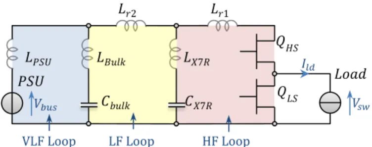
Fig. 1. Schematics of the converter under study: switching cell (𝑄𝑋),
bypass capacitors (𝐶𝑋), parasitic inductances (𝐿𝑋), input voltage (𝑉𝑏𝑢𝑠)
and output load.
Study of the Impedance of the Bypassing Network
of a Switching Cell – Influence of the Positioning of
the Decoupling Capacitors
YoannPascal Laboratory SATIE CNAM Paris, France firstname.name@satie.ens-cachan.fr Denis Labrousse Laboratory SATIE CNAM Paris, France firstname.name@satie.ens-cachan.fr Mickaël Petit Laboratory SATIE CNAM Paris, France firstname.name@satie.ens-cachan.fr François Costa Laboratory SATIE UPEC Créteil, France firstname.name@satie.ens-cachan.fr
Abstract—Mechanisms responsible for ringing and oscillations in power converters at transistors turn-offs are, first, studied using small signal modelling. It is explained why a 50 % derating must be applied to high-speed transistors. Experimental measurements validate the analytical predictions. The influence of the distance between a switching cell and its decoupling capacitors is then studied; it appears that using a low-inductance – though simple – layout results in a stray inductance as low as 11 nH when the capacitor is 30 cm away from the switching cell, enabling degrees of freedom for thermal management.
Keywords—bypass, DC-link capacitor, decoupling, GaN transistor, high speed switching, overvoltage, switching cell, switching transient
I. INTRODUCTION
Wide BandGap (WBG) devices are much faster than their silicon counterparts. Parasitic elements due to layout, connections and to components themselves result in voltage overshoots, oscillations and losses that drive designers to oversize devices – a costly measure. One way to limiting stray inductances consists in placing the devices as close as possible to one another. This, however, may result in poor thermal performances whilst complicating system integration. There is therefore a trade-off between thermal performances, electrical stress, and Electro-Magnetic Compatibility (EMC).
Reaching optimal designs requires a comprehensive and quantitative understanding of this trade-off.
The aim of this paper is two-fold. First, in section II, a simple and linear model of a switching cell is proposed so as to predict turn-off oscillations frequencies and amplitudes. Then, in section III, given a specific layout, the relationship between the loop inductance and the distance between the switching devices and its decoupling capacitors is experimentally studied. Section IV concludes the paper.
II. OSCILLATION MECHANISMS IN A SWITCHING CELL
A. Introduction
Many research papers have developed models aiming at predicting oscillations frequencies and amplitudes, either at turn-off [1]–[4] or turn-on [5], [6]. These studies usually model switching loops with laddered linear RLC circuits and current- or voltage- sources. Oscillations are studied either in time- [3], [4], [7]–[9] or frequency- [7], [10] domain.
These models, however, usually require an extensive knowledge of the circuit parasitic elements. Even if this can partly be inferred from simulations, accurate values – and especially damping coefficients in semiconductors – can be difficult to obtain, in particular due to their dependences with frequency, bias and temperature. Similar comments can be made regarding switching times.
So as to avoid the cumbersome and unreliable task of estimating switching times and resistances, the model developed in this paper assumes zero-switching times, i.e. that edges are infinitely steep. The circuit is then studied in a worst-case scenario, resulting in an over-estimation of the oscillations amplitudes. This assumption will nonetheless prove to be quite reasonable when dealing with fast, WBG, devices.
B. Modelling 1) Introduction
Let us consider (Fig. 1) a switching cell bypassed by two capacitors: a small one, 𝐶𝑋7𝑅, a priori ceramic-based, for
local bypassing, and a bulkier DC-link capacitor 𝐶𝑏𝑢𝑙𝑘. The
circuit is powered by a voltage source 𝑉𝑏𝑢𝑠 and supplies a
load modelled as a current source. Some lumped parasitic inductances are shown in Fig. 1. This figure also highlights three loops that may oscillate:
This work was supported by a grant overseen by the French National Research Agency (ANR-15-CE05-0010) – project HIT-TEMS.
𝐿𝑜𝑎𝑑 𝑉𝑠𝑤 𝐶𝑋7𝑅 𝐿𝑋7𝑅 𝐿𝐵𝑢𝑙𝑘 𝑄𝐿𝑆 𝐶𝑏𝑢𝑙𝑘 𝑄𝐻𝑆 𝐿𝑃𝑆𝑈 𝐿𝑟2 𝐿𝑟1 𝑃𝑆𝑈 𝑉𝑏𝑢𝑠 𝐼𝑙𝑑 HF Loop LF Loop VLF Loop
Fig. 2. Simplified schematic of the converter, with parasitic elements
Fig. 5. Simplified converter schematic during the voltage switching.
Fig. 4. Asymptotic impedance diagram of the bypass network (Fig. 3), seen from the load. 𝐿3= ∞, Log-log scale.
Fig. 3. Converter schematic with 𝑄𝐿𝑆 off and 𝑄𝐻𝑆 on.
- a High Frequency (HF) loop, including the switching cell itself and the local bypass capacitor;
- a Low Frequency (LF) loop, including both capacitors; - a Very Low Frequency (VLF) loop, including the
power source and the DC-link capacitor.
So as to simplify the analysis without losing the relevance of the study for field-use, it is assumed that the parasitic inductances fully decouple the loops: the oscillations can then be studied independently in each loop, which have distinct ringing frequencies and do not interfere. Papers have studied this matter, e.g. [7], [11]. The circuit of Fig. 1 can then be simplified (Fig. 2), were:
{𝐿2= 𝐿𝑟2+ 𝐿𝐿1𝑏𝑢𝑙𝑘= 𝐿+ 𝐿𝑟1+ 𝐿𝑋7𝑅𝑋7𝑅≈ 𝐿𝑟2+ 𝐿𝑏𝑢𝑙𝑘
𝐿3= 𝐿𝑃𝑆𝑈+ 𝐿𝑏𝑢𝑙𝑘
(1) are the HF, LF, and VLF loop inductances.
Furthermore, the equivalent circuit when 𝑄𝐿𝑆 is off and
the load current flows through 𝑄𝐻𝑆 is given in Fig. 3.
𝐶𝑜𝑢𝑡 models the parasitic capacitance of the switching node –
𝐶𝑜𝑢𝑡 is a priori mainly due to the output capacitance of 𝑄𝐿𝑆.
The asymptotic impedance diagram of the network, seen from the load is given in Fig. 4.
Loop capacitances can be defined as: {
𝐶1= (𝐶𝑜𝑢𝑡−1 + 𝐶𝑋7𝑅−1)−1≈ 𝐶𝑜𝑢𝑡
𝐶2= (𝐶𝑋7𝑅−1 + 𝐶𝑏𝑢𝑙𝑘−1 )−1≈ 𝐶𝑋7𝑅
𝐶3= 𝐶𝑏𝑢𝑙𝑘
(2) The series-resonant frequencies of the HF and LF loops are: 𝑓𝑟1= (2𝜋√𝐿1𝐶2) −1 , 𝑓𝑟2= (2𝜋√𝐿2𝐶3) −1 (3)
The parallel-resonant frequencies are: 𝑓𝑎,𝑖 = (2𝜋√𝐿𝑖𝐶𝑖)
−1
, 𝑖 ∈ ⟦1, 3⟧ (4)
Assuming that the loops are decoupled was justified since, a priori and due to component sizes:
𝐶𝑜𝑢𝑡≪ 𝐶𝑋7𝑅≪ 𝐶𝑏𝑢𝑙𝑘, 𝐿1≪ 𝐿2≪ 𝐿3 (5)
This leads to time-domain decoupling of transient phenomena – as will be detailed hereunder.
At 𝑄𝐿𝑆 turn-off (and, more generally, in a hard-switching
converter supplying an inductive load, at turn-off) the voltage is switched prior to current. Two transients, a voltage step and then a current one, are therefore generated, leading to oscillations due to distinct mechanisms. The next two subsections describe those mechanisms.
2) Voltage switching
During the first phase of the switching, the switching node voltage goes from 0 to 𝑉𝑏𝑢𝑠. During this phase, the
Low-Side (LS) transistor can be modelled as its output capacitance whereas the High-Side (HS) switch can be modelled as a voltage step going from 𝑉𝑏𝑢𝑠 to 0. This step
will excite the loops one after the other, propagating to the power supply.
During the first instant following the step, before notable oscillations can be observed in the LF loop (i.e. such that 𝑡 ≪ 𝑓𝑎2−1) and since 𝐶𝑜𝑢𝑡≪ 𝐶𝑋7𝑅, the voltage across 𝐶𝑋7𝑅
remains quite constant. The circuit can therefore be simplified as shown in Fig. 5. To put it another way: after the step and before the voltage across 𝐶𝑋7𝑅 has had time to
notably change, since 𝐶𝑜𝑢𝑡≪ 𝐶𝑋7𝑅, the circuit can be
simplified as shown in Fig. 5. The HF loop therefore oscillates at frequency 𝑓𝑎,1 and with amplitude 𝑉𝑏𝑢𝑠, the
voltage 𝑉𝑠𝑤 being expressed as:
𝑉𝑠𝑤= 𝑉𝑏𝑢𝑠⋅ (1 − cos(2𝜋𝑓𝑎1𝑡)) (6)
The overvoltage is then equal to 𝑉𝑏𝑢𝑠. In other word: the
peak voltage across 𝑄𝐿𝑆 is twice the input voltage.
The step then propagates to the other loops but with decreasing amplitude, yielding oscillations of negligible amplitudes.
If the quality factor 𝑄1 of the HF loop was not infinite,
one could show that the overvoltage would be given by: 𝑉̂𝑉,1= 𝑉𝑏𝑢𝑠⋅ 𝑒−𝜋 Λ⁄ , Λ = √4𝑄12− 1 (7) 𝐿2 𝑄𝐿𝑆 𝐶𝑋7𝑅 𝐶𝑏𝑢𝑙𝑘 𝑃𝑆𝑈 𝐿3 𝐿1 𝑄𝐻𝑆 𝐿𝑜𝑎𝑑 𝑉𝑠𝑤 𝑉𝑏𝑢𝑠 𝐼𝑙𝑑 HF Loop LF Loop VLF Loop 𝐿2 𝑄𝐿𝑆 𝐶𝑋7𝑅 𝐶𝑏𝑢𝑙𝑘 𝑃𝑆𝑈 𝐿3 𝐿1 𝑄𝐻𝑆 𝐿𝑜𝑎𝑑 𝑉𝑠𝑤 𝑉𝑏𝑢𝑠 𝐼𝑙𝑑 𝐶𝑜𝑢𝑡 𝐶𝑜𝑢𝑡 𝐿1 𝑉-𝑠𝑡𝑒𝑝 𝑉𝑏𝑢𝑠 𝑉𝑠𝑤 𝑓 ȁ𝑍ȁ 1 𝜔𝐶𝑏𝑢𝑙𝑘 𝜔𝐿2 1 𝜔𝐿1 𝜔𝐶𝑋7𝑅 1 𝜔𝐶𝑜𝑢𝑡 𝑓𝑟2 𝑓𝑎2 𝑓𝑟1 𝑓𝑎1
Fig. 8. Measured switching node voltage. Logarithmic X-scale. Fig. 6. Equivalent circuit during the current switching.
TABLE 1. Maximum rise time so that the steep-edge assumption is valid vs (𝐶𝑜𝑢𝑡, 𝐿1). 𝑪𝒐𝒖𝒕 𝑳𝟏 𝑡𝑟,𝑚𝑎𝑥𝑖 = 2√𝐶𝑜𝑢𝑡⋅ 𝐿1 100 pF 1 nH 0,63 ns 1 nF 1 nH 2 ns 1 nF 10 nH 6,3 ns 10 nF 100 nH 63 ns
Fig. 7. Measured switching node voltage (zero-padding interpolated). Log. x-scale.
3) Current switching
After the voltage is switched, the current switching occurs. During this transition, the High Side (HS) transistor can then be modelled by a short, the LS one by its output capacitance and the load by a current step – Fig. 6.
The current step will excite resonances, leading to oscillations, in the HF, LF and VLF loops one after the other, propagating from the switching node to the input power supply. Under the assumption that the loops are decoupled, each one can be modelled as a simple circuit with inductance 𝐿𝑖 (𝑖 ∈ ⟦1, 3⟧, cf. (1)), capacitor 𝐶𝑖 (𝑖 ∈ ⟦1, 3⟧, cf. (2)), and a
current step of amplitude 𝐼𝑙𝑑 in parallel. The oscillations have
frequencies 𝑓𝑎,𝑖 (4) and amplitude:
Δ𝑉𝐼,𝑖= 𝐼𝑙𝑑⋅ 𝑍𝑐,𝑖, 𝑍𝑐,𝑖= √𝐿𝐶𝑖
𝑖, 𝑖 ∈ ⟦1, 3⟧
(8) Where 𝑍𝑐 is the characteristic impedance of loop 𝑖.
C. Experimental validation
Voltage overshoots were measured on a prototype and compared to predictions from our model. An integrated GaN switching cell (LMG5200, 80 V – 10 A – 15 mΩ𝑡𝑦𝑝, from TI
[12]) was used. It was bypassed by a MKP DC-link capacitor ( 𝐶𝑏𝑢𝑙𝑘= 15 µF) together with a X7R-ceramic bypass
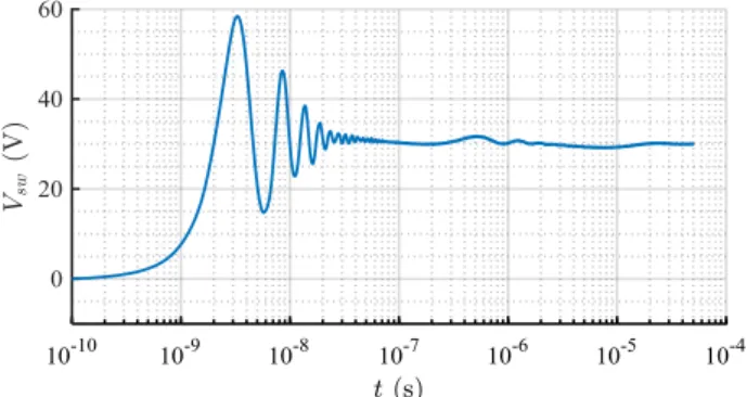
capacitor (𝐶𝑋7𝑅= 1 µF). The supply voltage was set to 𝑉𝑏𝑢𝑠 = 30 V . Typical switching waveforms are given in
Fig. 7. Three ringing periods can be seen, corresponding to the three loops: HF loop between 2 ns and 20 ns; LF loop between 100 ns and 2 µs; VLF loop between 2 µs and 20 µs.
The amplitudes of the HF and LF oscillations where measured for various load current values. As shown in Fig. 8, the amplitude of the measured HF oscillations (red squares) do not depend upon the load current 𝐼𝑙𝑑 and are very close to
the ones predicted by our model for the voltage switching (red line assuming 𝑄1= ∞, yellow line using the measured
𝑄1−value). On the other hand, the amplitude of the measure
LF oscillations (blue squares) increase linearly with 𝐼𝑙𝑑 (fit in
blue), with a slope 1.4 Ω – close to the value predicted by our
model for the current step (√ 𝐿2
𝐶𝑋7𝑅≈ √
22 nH
68 nF≈ 1.8 Ω).
It has also been observed that the amplitude and the frequency of LF oscillations have, as expected, a dependence in 𝐶𝑋7𝑅−0.5 whereas the HF oscillations do not depend on 𝐶𝑋7𝑅.
As a result, these measurements tend to validate the model developed in this section.
D. Discussion: on the steep-edge assumption
It has been assumed that edges have zero-rise time, which implies that the edges are fast enough to excite oscillations in the loops. Formally, this means that the bandwidth of the edges, with rise time 𝑡𝑟, is greater than the loop oscillation
frequency 𝑓𝑟𝑒𝑠. For the HF loop, this can be written:
1
𝜋𝑡𝑟> 𝑓𝑟𝑒𝑠⇔ 𝑡𝑟< 2√𝐶1⋅ 𝐿1 (9)
For various 𝐶𝑜𝑢𝑡 and loop inductance values, we give in
TABLE 1 the maximum rise time so that the assumption is valid. The first three lines correspond to cells using GaN transistors, lines number 2 and 3 are more related to SiC and Si MOSFETs whereas the last one is given for reference, corresponding to a traditional power module. It appears that the switching times calculated are similar to those that can be measured in prototypes, validating the assumption in the case of switching cells using fast, WBG, transistors.
E. Conclusion
The bypass network of a switching cell is composed of several loops that can oscillate when excited by switching events. A simple model that does not require extensive knowledge on the circuit under study whilst considering fast switching devices was developed. It shows that two mechanisms are involved in the oscillations: voltage and current switching. Both mechanisms yield to voltage
Fig. 9. Simplified circuit layout (bottom layer ground plane not shown).
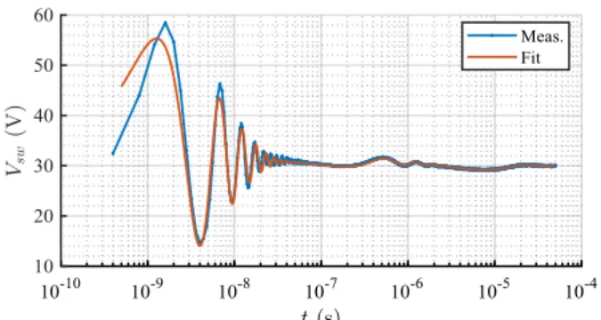
Fig. 10. Typical switching waveform: measurement (blue) and fit (red). 𝑛𝐿= 3. Logarithmic X-scale.
Fig. 11. HF loop inductance (𝐿1) vs. 𝑑𝑋7𝑅 and LF loop inductance (𝐿2)
vs. 𝑑𝑏𝑢𝑙𝑘. overshoots in the switching loops, with various amplitudes
and phase-shifts. Current switching yields oscillations with amplitude proportional to the switched current, whereas voltage switching yields oscillations with amplitude close to the switched voltage – i.e. close to the supply voltage. This last overshoot is highly detrimental since it requires a 50 % derating of the switch voltage rating. Assuming a minimal loop inductance, little can be done to avoid this overshoot but slowing down the switch (e.g. by artificially increasing the gate resistance) or increasing the cell output capacitance. III. ON THE INFLUENCE OF THE DISTANCE BETWEEN BYPASS
CAPACITORS AND SWITCHING CELLS
A. Introduction
Being able to put bypass capacitors at some distance from the switching cell would simplify circuit design and reduce cost. As a matter of fact, it would enable several cells to share decoupling capacitors and heatsinks while loosening thermal constrains. It would also simplify mechanical designs and allow manufacturing circuits with unconventional form-factors.
This study aims at understanding to what extent the distance between a switching cell and its decoupling capacitors can be increased without excessively degrading EMC or increasing either thermal or electrical stress. To this end, the relationship between loop inductance and distance between a switching cell and its decoupling capacitors is studied.
To this end, a switching cell was built its output voltage measured given various decoupling network arrangements.
B. Circuit under study
An integrated GaN half bridge (LMG5200, 80 V – 10 A – 15 mΩ𝑡𝑦𝑝, from TI [12]) was used; dead-times were set to
5 ns. Its power supplied was decoupled by a DC-link capacitor (875 V – 15 µF, MKP, ref. B32678G8156K000 [13]) and a ceramic local bypass capacitor (X7R, 470 nF – 1 kV, ref. 2220Y1K00474KXTWS2). A 70 mm-wide, not terminated, Edge Coupled Microstrip transmission line was used between the capacitor and the switching cell. The distance between the decoupling capacitors and the cell are 𝑑𝑏𝑢𝑙𝑘 and 𝑑𝑋7𝑅 (Fig. 9). The circuit was manufactured using
the top-copper layer of a 35/370/35 µm-thick FR4-based PCB, the bottom copper layer being used as a ground plane. The circuit was powered by a voltage source 𝑉𝑏𝑢𝑠= 30 V. It
was used in a double pulse test, supplying a broadband inductive load with a current 𝐼𝑙𝑑= 5 A.
C. Measurement method
The switching node voltage was measured using a Teledyne-Lecroy HDO8108 oscilloscope (12 bit, 1 GHz, 2.5 GSa/s) and a PP008 10:1 passive voltage probe (500 MHz, 10 MΩ//9.5 pF), connected to the circuit with an ad-hoc, low-inductance setup [11].
The capacitances 𝐶𝑜𝑢𝑡, 𝐶𝑏𝑢𝑙𝑘 and 𝐶𝑋7𝑅 were measured
using an E4990a impedance analyser, at 100 kHz and at 30 V biasing voltage:
𝐶𝑋7𝑅,30V𝑑𝑐= 447 nF, 𝐶𝑏𝑢𝑙𝑘,30V𝑑𝑐= 14.88 µF,
𝐶𝑜𝑢𝑡,30V𝑑𝑐= 571 pF
(10) A model describing the oscillations of 𝑛𝐿 loops:
𝑉𝑠𝑤∗ = 𝑉𝑑𝑐+ ∑ 𝑉̂𝑘⋅ 𝑠𝑖𝑛(𝜔𝑘𝑡 + 𝜙𝑘) ⋅ 𝑒−𝑡/𝜏𝑘 𝑛𝐿 𝑘=1 , 𝛽 = [𝑉𝑑𝑐, 𝑉̂𝑘, 𝜔𝑘, 𝜙𝑘, 𝜏𝑘]𝑘 (11)
was then fitted on the measurements, the vector 𝛽 being used as fitting parameter. The 𝜔𝑘 and capacitances values
were then used to estimate the loop inductances using Thomson’s formula [14], (3)-(4).
Model (11) appeared to be a good fit for the measurements (Fig. 10), the capacitances nonlinearities having limited impact on the result.
D. Loop inductance 1) LF Loop
The effect of the distance 𝑑𝑏𝑢𝑙𝑘 between the switching
cell and the DC-link capacitor on the LF loop inductance was studied at 𝑑𝑋7𝑅 = 0 (Fig. 11). As expected, 𝐿2 increases
with 𝑑𝑏𝑢𝑙𝑘, due to the increase of the loop area. The rise is
𝑑𝑏𝑢𝑙𝑘 goes from 0 to 260 mm. Furthermore, the capacitor
self-inductance (ESL: 𝐿𝑏𝑢𝑙𝑘= 18.4 nH) accounts for up to
66 % of the overall loop inductance.
2) HF Loop
The DC-link capacitor having been removed from the circuit (i.e. 𝑑𝑏𝑢𝑙𝑘= ∞), the impact of 𝑑𝑋7𝑅 on the HF Loop
inductance was studied (Fig. 11). These measures show that the smallest achievable inductance is 1.2 nH and that the increase of 𝐿1 vs. 𝑑𝑋7𝑅 is very slow: 0.3 nH/cm.
The HF loop inductance is then only 11 nH when the switching cell is 30 cm away from its bypass capacitor.
E. Small signal measurements
Another prototype was manufactured, with layout similar to the first one but incorporating a factice switching cell, with 𝑄𝐿𝑆 replaced by its output capacitance and 𝑄𝐻𝑆 shorted.
The impedance seen from the load was then measured using an E4990a impedance analyser (stimuli amplitude: 500 mV, no bias). The linear model from Fig. 3 was then fitted on the measurements.
The measured inductances were in good agreement with those obtained with the first prototype. In particular the same slope of 0.3 nH/cm was found. Though, an offset due to the use of a factice switching cell, with geometry different from that of the real one, was found.
F. Conclusion
This study dealt with the influence of the distance between a switching cell and its decoupling capacitors.
As expected, minimising inductances requires to put components as close to one another as possible. However, this study showed that the simple layout we used made loop inductances little sensitive to the distance between the cell and the decoupling capacitors.
Using a thin and grounded PCB is of primal importance to limit loop inductances. Furthermore, a capacitor’s ESL can account for a major part of the overall loop inductance.
This study shows that, using the layout under study, the loop inductance sensitivity to the distance between a switching cell and its decoupling capacitors is rather low (about 300 pH/cm). Additionally, it showed that the DC-link capacitor can be placed quite far from the cell. These results highlight the relative freedom designers have regarding the arrangement of the components of a switching cell and its bypass network, thus facilitating, in particular, thermal design.
IV. CONCLUSION
The first part of this study shows that, for devices with fast enough switching speeds, two mechanisms must be considered to predict oscillations. The first one results in an overvoltage that is as high as the full bus voltage 𝑉𝑏𝑢𝑠
whereas the other one induces an overvoltage of amplitude proportional to the load current.
The distance between the switching cell and its decoupling capacitors was then varied and the resulting stray inductance was measured both in frequency- and time- domains, using either an impedance analyser or an oscilloscope. The results show that the stray inductance remains rather low (< 11 nH) even when the capacitor is far away from the switching cell (30 cm). Furthermore, the
sensitivity of this inductance vs. the distance is very low: about 0.3 nH/cm. Choosing a capacitor with low self-inductance (ESL) is therefore most important so as to limit the overall loop inductance. Constrains on the compactness may then, in some cases, be loosen so as to improve thermal management and system integrability.
V. REFERENCES
[1] W. Zhang, Z. Y. Zhang, F. Wang, L. M. Tolbert, D. Costinett, and B. Blalock, ‘Characterization and Modeling of a SiC MOSFET’s Turn-Off Overvoltage’, Mater. Sci. Forum, vol. 924, pp. 827–831, Jun. 2018. [2] J. Wang, H. S. Chung, and R. T. Li, ‘Characterization and Experimental Assessment of the Effects of Parasitic Elements on the MOSFET Switching Performance’, IEEE Trans. Power Electron., vol. 28, no. 1, pp. 573–590, Jan. 2013.
[3] Z. Zhang, F. Wang, L. M. Tolbert, B. J. Blalock, and D. Costinett, ‘Understanding the limitations and impact factors of wide bandgap devices’ high switching-speed capability in a voltage source converter’, in 2014 IEEE Workshop on Wide Bandgap Power Devices and
Applications, Knoxville, TN, USA, 2014, pp. 7–12.
[4] W. Teulings, J. L. Schanen, and J. Roudet, ‘MOSFET switching behaviour under influence of PCB stray inductance’, in IAS ’96.
Conference Record of the 1996 IEEE Industry Applications Conference Thirty-First IAS Annual Meeting, San Diego, CA, USA, 1996, vol. 3, pp.
1449–1453.
[5] J. Williams and D. Beebe, ‘Diode Turn-On Time Induced Failures in Switching Regulators’. Linear Tech., Jan-2009.
[6] W. Zhang, Z. Zhang, F. Wang, D. Costinett, L. M. Tolbert, and B. J. Blalock, ‘Characterization and Modeling of a SiC MOSFET’s Turn-On Overvoltage’, in 2018 IEEE Energy Conversion Congress and
Exposition (ECCE), Portland, OR, 2018, pp. 7003–7009.
[7] L. Li, P. Ning, Z. Duan, D. Zhang, and X. Wen, ‘A study on the effect of DC-link decoupling capacitors’, in 2017 IEEE Transportation
Electrification Conference and Expo, Asia-Pacific (ITEC Asia-Pacific),
Harbin, China, 2017, pp. 1–5.
[8] T. Li, J. Wang, and H. S. Chung, ‘Effect of parasitic elements in a power converter on the switching performance of a MOSFET-snubber-diode configuration’, in 2011 Twenty-Sixth Annual IEEE Applied Power
Electronics Conference and Exposition (APEC), Fort Worth, TX, USA,
2011, pp. 364–371.
[9] J. B. Witcher, ‘Methodology for switching characterization of power devices and modules’, M. Sc. Thesis, Jan. 2002.
[10] Z. Chen, D. Boroyevich, P. Mattavelli, and K. Ngo, ‘A frequency-domain study on the effect of DC-link decoupling capacitors’, in
2013 IEEE Energy Conversion Congress and Exposition, Denver, CO,
USA, 2013, pp. 1886–1893.
[11] Z. Zhang et al., ‘Methodology for switching characterization evaluation of wide band-gap devices in a phase-leg configuration’, in 2014
IEEE Applied Power Electronics Conference and Exposition - APEC 2014,
Fort Worth, TX, USA, 2014, pp. 2534–2541.
[12] ‘LMG5200 Datasheet’. Texas Instrument, Oct-2018. [13] ‘MKP Film Capacitors, series B32674-8’, 2017.
[14] W. Thomson, ‘On Transient Electric Currents’, Phil Mag, vol. 5, pp. 393–405, Jun. 1853.