HAL Id: hal-02030568
https://hal.archives-ouvertes.fr/hal-02030568
Submitted on 25 Aug 2020HAL is a multi-disciplinary open access archive for the deposit and dissemination of sci-entific research documents, whether they are pub-lished or not. The documents may come from teaching and research institutions in France or abroad, or from public or private research centers.
L’archive ouverte pluridisciplinaire HAL, est destinée au dépôt et à la diffusion de documents scientifiques de niveau recherche, publiés ou non, émanant des établissements d’enseignement et de recherche français ou étrangers, des laboratoires publics ou privés.
Doping as a strategy to tune color of 2D colloidal
nanoplatelets
Marion Dufour, Eva Izquierdo, Clément Livache, Bertille Martinez, Mathieu
Silly, Thomas Pons, Emmanuel Lhuillier, Christophe Delerue, Sandrine
Ithurria
To cite this version:
Marion Dufour, Eva Izquierdo, Clément Livache, Bertille Martinez, Mathieu Silly, et al.. Doping as a strategy to tune color of 2D colloidal nanoplatelets. ACS Applied Materials & Interfaces, Washington, D.C. : American Chemical Society, 2019, 11 (10), pp.10128-10134. �10.1021/acsami.8b18650�. �hal-02030568�
Doping as Strategy to Tune Color of 2D colloidal Nanoplatelets
Marion Dufour
1, Eva Izquierdo
1, Clément Livache
1,2, Bertille Martinez
1,2, Mathieu G. Silly
3, Thomas
Pons
1, Emmanuel Lhuillier
2, Christophe Delerue
4, Sandrine Ithurria
1 *1
Laboratoire de Physique et d’Etude des Matériaux, ESPCI-ParisTech, PSL Research University,
Sorbonne Université UPMC Univ Paris 06, CNRS, 10 rue Vauquelin 75005 Paris, France.
2
Sorbonne Universités, UPMC Univ. Paris 06, CNRS-UMR 7588, Institut des NanoSciences de
Paris, 4 place Jussieu, 75005 Paris, France
3
Synchrotron-SOLEIL, Saint-Aubin, BP48, F91192 Gif sur Yvette Cedex, France
4
Université de Lille, CNRS, Centrale Lille, ISEN, Université de Valenciennes, UMR 8520-IEMN,
59000 Lille, France
Abstract : Among colloidal nanocrystals, 2D nanoplatelets (NPL) made of II-VI compounds, appear as a special class of emitters with especially narrow photoluminescence signal. However the PL signal in the case of NPL is only tunable by discrete step. Here we demonstrate that doping is a viable path to finely tune the color of this NPL from green to red, making them extremely interesting as phosphor for wide gamut display. In addition using a combination of luminescence spectroscopy, tight binding simulation, transport and photoemission, we provide a consistent picture for the Ag doped CdSe NPL. The Ag state is strongly bound and located 340 meV above the valence band of the bulk material. The Ag dopant shifts the Fermi level toward the valence by up to 400 meV but preserve the n-type nature of the material.
Keywords : nanoplatelets, doping, gamut, luminescence
INTRODUCTION
In NPLs, in contrast to quantum dots or rods, the charge carriers are confined only along the thickness direction, which is atomically flat and homogeneous within a NPL population. This completely eliminates inhomogeneous broadening and yields the narrowest photoluminescence linewidth among colloidal semiconductor nanocrystals. Thanks to this narrowness and their fast photoluminescence lifetime, NPLs have been used for a broad range of applications from light emitting diode1,2,3, to transistor4, detector5, phototransistor6, solar light concentrator7 and laser8,9. On the other hand, contrarily to colloidal quantum dots (CQDs), the spectrum of NPL can only be tuned in discrete steps corresponding to the finite number of atomic planes in the thickness direction. 10 Typically NPL made of CdSe present their first excitonic peaks at 390 nm, 460 nm, 510 nm, 550 nm as the thickness increases from 2 to 5 layers of selenium. To obtain more tunability, alloyed NPL11,12, for example made of CdSSe2, have been reported. In this paper we explore the possibility to use doping as a viable path to tune the emission of CdSe NPL from green to red.
Doping has for long been extremely challenging from a synthetic point of view13. Mn doping14 is probably one of the most established method. In the case of wide band gap semiconductor, an energy transfer from the band edge to the Mn 3d state leads to the observation of the Mn2+ phosphorescence15. Similarly, electron injection with CQD16 is known to lead to an electrochromic feature17 through a bleach of the band edge transition and the appearing of mid IR intraband absorption18.
Extrinsic impurities can also be integrated as a path to introduce traps within the band gap which will tune the exciton energy. This method is widely used in the case of CIGS (CuInGaS(e)) nanocrystals for which the emission involves Cu states19–22. Similarly, the involvement of Cu states in the emission of Cu-doped CdSe material23 has been reported including in the case of NPL7,24. In this case the Cu atoms are introduced in the Cu+ form though a cation exchange process25. Other metals with a +I oxidation state, typically Ag+, have also been investigated as possible dopants for CdSe, in particular by the Norris group26,27,28. They reported that Ag behaves as n-type dopant at low doping and switches to a p type dopant when large amounts of dopant (>2 Ag per CQD) are incorporated29. They also reported that the introduction of Ag leads to an enhancement of the photoluminescence (PL) quantum efficiency. At low temperature, they observed the apparition of a second emission peak that is red shifted compared to the band edge and attributed to Ag states. However they have been unable to clearly conclude about the strength (weakly vs strongly bound) of exciton-Ag interaction. Cation exchange with silver30 and other noble metals have also been investigated on CdSe NPL beyond the doping regime, where metal tips start to form on the NPL31,32 corners, which may present interesting properties for transport33 and (photo)catalytic applications34. Here, we explore silver doping on CdSe 2D NPL in the intermediate doping regime from 1 to 100 Ag dopant per nanoparticle. We bring evidence that the 2D NPL present a significant difference with Ag doped CdSe CQD. The paper is organized as follows. The first part is a discussion on the optical properties of the Ag doped CdSe NPLs which highlights the potential of doping as a strategy to tune their emission spectrum. In the second part we discuss the energy position of the Ag level within the band gap of CdSe and demonstrate that the energy level of the Ag state lies at 0.34 eV above the bulk valence band, independently of doping concentration. Finally, using transport measurements and X-ray photoemission spectroscopy, we further discuss the impact of the Ag doping on the electronic structure of the material.
METHODS CHEMICALS
Octadecene (ODE) (Aldrich, 90 %), Cadmium acetate dihydrate Cd(Ac)2,2H2O (Strem, 98 %), Cadmium oxide (Strem, 99.99 %), Myristic acid (Aldrich, >99%), Oleic acid (OA) (Aldrich 90 %), Selenium (Strem Chemicals 99.99 %), Hexane (VWR, 99 %), Ethanol (VWR, 95-97 %), Silver (I) Behenate (Alfa, 94%), Propionic acid (Aldrich, 99%), Oleylamine (OLA) (Acros, 80−90%), Trioctylphosphine (TOP) (Cytec, Solvay),Tributylphosphine (TBP) (Cytec, Solvay), 1,2-ethanedithiol (EDT) (Fluka, 98.0%), LiClO4 (Aldrich, 98%), polyethylene glycol MW = 6 kg.mol−1 (PEG 6k) (Fluka), Octane (SDS, 99%), sulfur (Sigma, 99.99%), methanol (Carlo Erba, 99.9%), N-methylformamide (NMF) (Carlo Erba, 99%), sodium borohydride (NaBH4) (Sigma, 99%).
PRECURSOR PREPARATION
Cadmium myristate Cd(Myr)2: In a 50 mL three neck flask, 2.56 g of CdO and 11 g of myristic acid are mixed and degassed for 30 minutes at 80 °C. Then, under and argon flow, the temperature is set at 200 °C. The reaction is stopped when the solution becomes colorless (approximately 40 minutes). At 60 °C, 30 mL of methanol are added to solubilize the excess of myristic acid. The cadmium myristate is then washed 5 times with methanol. It is finally dried overnight under vacuum at 70 °C.
Silver Oleate 1 mM: In a flask, 5 mg of silver behenate and 1 mL of OA are sonicated and then heated with a heat gun until all the silver behenate is solubilized. Then, 10 mL of ODE are added to have a final concentration of Ag of 1 mM. NANOCRSYTAL SYNTHESIS
CdSe 4ML synthesis: In a 50 mL three neck flask, 24 mg of Se, 340 mg of Cd(Myr)2 and 25 mL of ODE are mixed and degassed under vacuum at room temperature for 20 minutes. Then, under an argon flow, the temperature is set to 240 °C. At approximately 200 °C, when the solution turns orange, 110 mg of Cd(Ac)2,2H2O are swiftly added. The temperature is held at 240 °C for 10 minutes. Then, 500 µL of OA is added and the solution is quickly cooled to room temperature. After adding 25 mL of hexane and 25 mL of ethanol, the nanoplatelets are precipitated at 6000 rpm for 5 minutes. Then, the supernatant composed of dots is discarded and the nanoplatelets are redispersed in 20 mL of hexane.
Ag doping: In a flask with a stirring magnet, we add 1 mL of 4 ML nanoplatelets and 2 mL of hexane. A second solution of x mL of Silver Oleate 1 mM and (3-x) mL of hexane is prepared (x ranging from 0.01 to 1). 2.5 mL of this second solution is added to the first one at a rate of 6 mL/h. The progressive addition ensures a doping as homogeneous as possible. The solution is used as obtained for PL measurements. A washing step with ethanol is used for the other characterizations. For the other thicknesses of NPLs, the protocol is the same but the amount of NPL can vary a little: 2 mL for 2 and 5 MLs, 500 µL for 3 MLs and 1 mL for 6 ML NPLs
MATERIAL CHARECTERIZATION
UV-visible: spectra have been acquired with a Shimadzu UV-3600 spectrometer. Photoluminescence and excitation spectra are obtained from an Edinburgh Instrument spectrometer.
A JEOL 2010 The transmission electron microscope is used to image nanoparticles and is operated at 200 kV. The grids are prepared by a dropcast of a solution of NPLs dispersed in hexane and degassed overnight under secondary vacuum.
Transistors measurements
Electrodes are made using standard optical lithography methods. Briefly the surface of a Si/SiO2 (400 nm thick) wafer is cleaned by sonication in acetone. The wafer is rinsed with isopropanol and finally cleaned using a O2 plasma for 5 min. AZ5214 resist is spin-coated and baked at 110 °C for 90 s. The substrate is exposed under UV through a pattern
mask for 1.5 s. The film is further baked at 125 °C for 2 min to invert the resist. Then a 40 s flood exposure is performed. The resist is developed using a bath of AZ726 for 32 s, before being rinsed with pure water. We then deposit a 5 nm Cr layer and a 80 nm gold layer using a thermal evaporator. The lift-off is performed by dipping the film for 1 h in acetone. The electrodes are finally rinsed using isopropanol and dried by air flow. The electrodes are 2.5 mm long and spaced by 10 μm.
Electrolyte: 0.5 g of LiClO4 are mixed with 2.3 g of PEG on a hot plate in an Ar filled glove box at 170 °C for 2 h. Transistor preparation: At the end of the partial cation exchange, the particles are precipitated once and redispersed in hexane/octane 9:1. This solution is dropcasted on an electrode in the glovebox. A solid state ligand exchange is then used to remove long carboxylate chains. It consists in dipping the film in a solution containing EDT in ethanol for 1.5 min. The film is then rinsed by dipping in ethanol for 30 s. Three drops are deposited with intermediary ligand exchange to avoid cracks and ensure a good coverage of the electrodes. Then, a drop of the electrolyte previously heated at 100 °C is deposited on the nanoparticle film.
Measurement: Transfer curves are acquired using a keithley 2400 as sourcemeter by setting the drain voltage to 100 mV and sweeping the gate voltage from -1 V to 3 V at a 1 mV/s rate.
XPS measurements
Sample preparation: Silicon wafers were rinsed with acetone, sonicated, rinsed again with acetone and iso-propanol and cleaned with a plasma cleaner for 5 minutes, with a plasma power of 7 W. 5 nm of Cr and 80 nm of Au were deposited using thermal evaporation deposition. A film of EDT caped NPLs is deposited on the substrate using the procedure described for transistors .
Measurements have been conducted on Tempo beamline of synchrotron Soleil. The film is then introduced in the preparation chamber and then degassed until a vacuum in the 10-10 mbar range is reached. The sample is finally introduced in the analysis chamber. During the XPS measurements, the photoelectrons were detected at normal emission and at 46° from the polarization vector 𝐸⃗ . Photon energy is set at 600 eV. For the photoelectrons analysis we use a 50 eV pass energy.
Simulation
The electronic structure of CdSe NPLs was calculated using a well-established atomistic tight-binding approach. Each Cd or Se atom is described by a set of 20 atomic orbitals, sp3d5s* for each spin degree of freedom where s* represents a second s orbital. The dangling bonds at NPL surfaces are saturated by pseudo-hydrogen (H) atoms described by a single s orbital for each spin orientation. The hopping terms in the hamiltonian matrix are restricted to nearest-neighbor interactions. Spin-orbit coupling is included. We used the tight-binding parameters of Ref.35 for zinc-blende CdSe. In this set of parameters, we have changed the value of the onsite s energy (Es) on Cd atoms to
-2.070 eV (instead of -1.857148 eV) because it gives a bulk CdSe bandgap of 1.66 eV (instead of 1.82 eV). It is important to mention that the experimental value of the bulk bandgap is not known with accuracy for CdSe in its zinc-blende phase. A value of 1.66 eV, already reported in Ref. 36, is more compatible with the optical gaps measured on thick CdSe NPLs (at 300K) and extrapolated to the bulk limit (see figure 2a). The Cd-H interaction terms simulate the effects of the ligands on the Cd atoms at the surface. The influence of ligands on the bandgap is non negligible, especially on the thinnest NPLs. Using Es(H) = 0.0 eV, Vsss = -2.5 eV and Vsps = +4.5 eV (notations of Ref.35), we obtain
for the thinnest NPL (3 ML) a gap in excellent agreement with experiments. The comparison between single-particle (tight-binding) gaps and measured optical gaps is pertinent because there is a substantial cancellation between self-energy and excitonic corrections in the ground excitonic state 37 for reasons discussed in Refs.38,39.
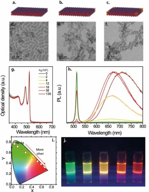
We first synthesize 4ML CdSe NPLs made of 5 planes of cadmium alternated with 4 planes of selenium using the procedure given by Ithurria et al40, see Figure 1a for a scheme of the nanoparticle. Structurally speaking these NPLs are 1.2 nm thick while their lateral extension have a rectangular aspect of 9 nm x 30 nm, as show in the transmission electronic microscopy (TEM) image in Figure 1d. The NPLs spectrum is given in Figure 1g and presents an excitonic feature at 510 nm.
To dope the NPLs with Ag+, we progressively add a solution of silver oleate (1 mM) diluted with hexane to a solution of NPLs under stirring. The addition is done drop by drop to achieve the best homogeneity. We then measure the amount of Ag atoms per nanoparticle using Inductively Coupled Plasma (ICP). This number increases progressively in the range from 1 to 100 Ag atom(s)/NPL and is in a good agreement with the amount of added Ag precursors (see supporting information).
By doping the NPL, the shape of the NPLs remains unaffected, see TEM images in Figure 1e and f. At low doping the presence of Ag is noticeable by TEM. On the other hand, when more than 100 Ag/NPL are introduced, tips start to form on the corners of the NPLs, consistently with previous reports31,Erreur ! Signet non défini.33,34 relative to metallic tip functionalized NPL, see Figure 1c and f.
Figure 1 Scheme of CdSe 2D NPL without (a) and with various amount of Ag (b and c), d. e and f are TEM image of 2D CdSe NPL with an increasing amount of silver per NPL (0, 18, 139). g. Absorption spectra of CdSe NPL for various amount of Ag doping. h. Photoluminescence spectra of CdSe NPL for various amount of Ag doping. i. Chromaticity diagram highlighting the position associated with the PL spectra of CdSe NPL with various amount of Ag doping. j. image of CdSe NPL solution with various amount of Ag doping
Optically speaking the absorption spectra of the NPLs remain totally unaffected by the introduction of Ag doping atoms, see Figure 1g. The intensity and positions of the first two optical features, which appear respectively at 510 and 480 nm and are related to heavy hole to conduction band and light hole to conduction band transitions40 remain unchanged. On the other hand, the photoluminescence (PL) spectrum is drastically affected by the presence of Ag. Without doping the CdSe NPLs present a very narrow feature at 510 nm with a full width at half maximum (FWHM) of 8 nm. When silver is introduced, a broad band (FWHM= 138 nm) appears that is red shifted compared to the excitonic peak, with an emission maximum at 660 nm. This result is quite different from what Sahu et al reported in the case of Ag doped CdSe CQD, where this red peak emission was only noticeable at low temperature (10K)Erreur ! Signet non défini.29
. In their work, the room temperature emission was only due to band edge recombination. In this sense our results are close to those reported by the Demir’s group for Cu+ doped CdSe NPL7,Erreur ! Signet non défini.24 where a red shifted emission was already observed at room temperature. On the other hand, Demir’s group focused on the large doping range to boost the Stokes shift, which is of utmost interest for solar concentrator applications. Thus, in their case the color promptly switched from green to red. By finely tuning the amount of dopant, we demonstrate that it is possible to finely tune the emission color from green to yellow, orange and finally red, see Figure 1i and j. This material is quite promising for display application, since once combined with a blue LED, it will enable very broad color gamut, thanks to the narrowness of the green emission of the NPL.
It should be pointed out that Sahu et al.29 reported an increase of the PL quantum yield (QY) while introducing 1 to 2 atoms of silver per particle. They attributed this enhancement to the effect of the electrostatic field created by the presence of the impurity in addition of the extra carrier addition. More recently Morgan et al.41 demonstrated that 1 to 2 atoms of silver per CQD could diminish the amount of hole trapping however such behavior was not seen in the case of CQD passivated with oleylamine. Thus it seems that this enhancement is mostly due to surface passivation and in particular non passivated selenium surface atoms. In the case of NPLs we never observed such QY enhancement. Firstly, the way the NPLs are doped is different. In order to prevent the fast diffusion of silver and a reorganization of the NPLs, we used slow addition of silver carboxylate instead of a mixture of silver precursor in presence of phosphine. This ensures the preservation of the carboxylate ligands of the native NPLs. Indeed, modification of the surface chemistry of NPLs has drastic effects on the optical features of NPLs.42 Secondly, in 9 nm x 30 nm 4ML CdSe NPLs, the top and bottom surfaces represent close to 85% of the total surface and are the cadmium rich [001] facets. Each of the cadmium are passivated by a carboxylate. Regarding the shape of the NPLs, the edges facets are also probably [100] and [010] facets which mean that they are also passivated by carboxylates, thus it brings just little space for non passivated selenium of surface.
In addition to tune the apparent color of the NPL emission, the bicolor spectrum enables us to evaluate the homogeneity of the doping within the NPL population. We used fluorescence cross correlation spectroscopy (FCCS) on a sample presenting approximately 15 Ag/NPL to measure the correlation between the band edge ( = 510 nm) and the dopant ( = 660 nm) emission. The results (see SI) show that (i) no NPLs emit only from the band edge state and (ii) 90 to 95% of NPLs emit only from the dopant state, while the rest emit from both the band edge and dopant states. This demonstrates that all NPLs are doped.
To clearly state about the potential of doping as a viable path to tune the color of semiconductor nanoparticle, it is critical to demonstrate that the method is not limited to CdSe NPLs with this specific thickness. In the supporting information we provide evidence for the presence of a similar red emission for other thickness of CdSe NPLs (see figure S8) and other compositions (CdS, see figure S9). In all these NPLs, similarly to CQDs, the broad redshifted emission originates from a metal to conduction band transition recombination. The origin of this broad PL band shape has been attributed by Nelson et al.43 to a strong vibronic coupling between the symmetric contraction and symmetry breaking Jahn-Teller distorsion in the [AgSe4] excited cluster. In NPLs the silver dopant is especially close to the surface as the NPLs are thin. In addition, the ligands induce stress on the surface of NPLs, leading to NPL folding and twisting to release this elastic energy. This lattice distortion is especially large for thin NPLs. This yields to a large distortion of the tetrahedral environment of the silver dopant and might explain why while increasing the NPLs thickness we observe a narrowing of the dopant emission width (see figure S8).
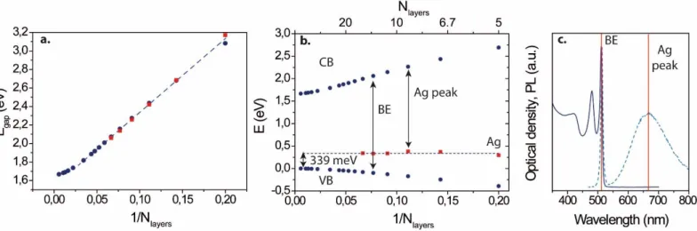
In the second part of the paper, we discuss the location of the Ag state within the CdSe band gap. The scaling of the band edge energy with thickness present a 1/N dependence with N the number of atomic plane in the NPL44, see Figure 2a. It results from a combination of quantum and dielectric confinements45. Thus contrary to what is expected for quantum well text book, the energy of the colloidal NPLs bands doesn’t scale a 1/N2 dependence in the case of ultrathin nanoparticles. Using a tight binding approach (see supplementary information), with, as only adjustable parameter, the nature of the orbitals ligands and their energies level estimated from the thinnest NPLs, we determine the gap of the NPLs. We indeed observe a linear dependence as function of 1/N (see figure 2a). From this, it was then possible to plot the theoretical dispersion of both the valence and conduction band independently (see figure 2b). We then reported the silver state for all 5 different populations of doped CdSe NPLs assuming that the broad PL transition results from a recombination of the conduction band to the silver state. By doing so, we observe that the Ag energy state is independent of confinement and is found to be 339 meV above the bulk valence band.46 In other word the energy of the silver state is constant with respect to vacuum, which is a clear signature of its strongly bound character. This contrasts with the case of spherical QD for which the binding of the Ag state has been found to be rather weakErreur ! Signet non défini.29. This difference of bonding in the case of NPL is likely at the origin of the observation of the red emission already at room temperature.
Figure 2 a band edge energy as a function of the inverse of the NPL thickness. b. Conduction, valence band and silver state energy as a function of the inverse of the NPL thickness. c Absorption and PL spectra for a given silver doping of 2D CdSe NPL, highlighting how the experimental band edge and conduction to silver state energy are determined.
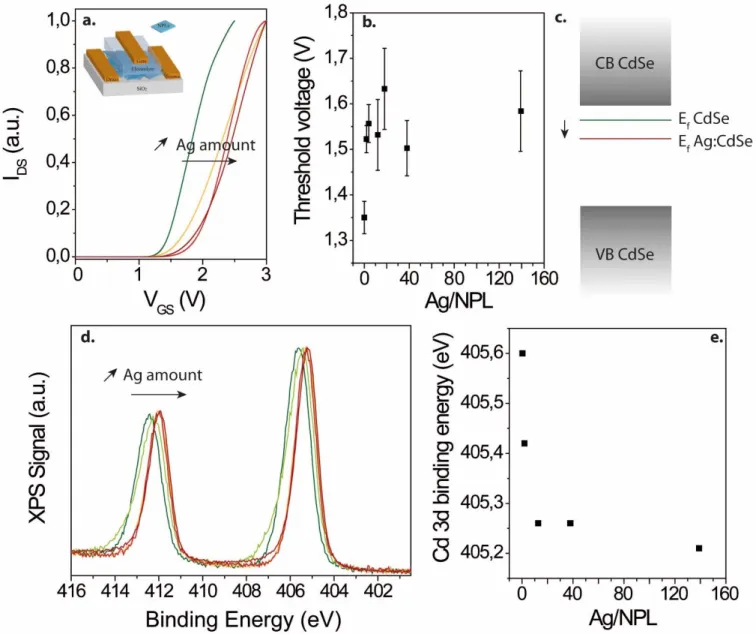
To complete the understanding of the electronic spectrum of Ag doped CdSe NPL we want to determine the position of the Fermi level and determine its shift with the doping. To do so, we use a combination of transport and photoemission measurements. For transport, we conduct measurement into an ion gel electrolyte configuration4,28 which is the only strategy to tune the doping magnitude up to several carrier per nanocrystals. In addition ion gel gating allows air operation and low operating bias. See the inset of Figure 3a for a scheme of the device. In all case the material present a n-type character, see Figure 3a, with an increase of the conductance under electron injection (ie under positive gate bias). We also observe a shift of the threshold voltage toward more positive value as Ag doping increase, in agreement with previous results by Sahu et alErreur ! Signet non défini.28,29, see Figure 3b. This shift is a signature of the displacement of the fermi level more deeply within the band gap of CdSe, see Figure 3b. Thus it is important to mention that CdSe due to its slight Cd rich character is a n-type material and will remain n-type even after the introduction of Ag traps state close to the valence band.
Figure 3 a. Drain current as a function of gate bias for thin film of CdSe NPL doped with various amount of Ag. The inset is a scheme of the used electrolytic transistor configuration. b. Threshold bias of the transfer curve as a function of the silver doping. c Scheme of the position of the Fermi level with and without silver doping with respect to valence and conduction band. d. Photoemission signal associated with the Cd 3d state for various amount of Ag doping. e. Binding energy of the Cd 3d state as a function of the silver doping.
Photoemission is also a very efficient tool to probe the electronic environment of nanocrystals. On the photoemission overview spectrum no signature of Ag peak has been observed unless the doping ratio reach 100 dopant per nanoparticle (see figure S6). On the other hand we observe a clear shift of the Cd 3d state with the introduction of silver, see Figure 3d. In CdSe, the excess of Cd is responsible for the n-type nature of the material. As Ag is introduced, the Cd 3d state shift toward lower binding energy, meaning that Cd2+ become more electron rich and now behave as Cd2+-δ.47 Thus the doped material is behaving as if the excess of Cd was reduced and thus a lower n-type doping is expected. Assuming a rigid shift of the whole photoemission spectrum with doping, we can estimate the shift of the Fermi level with doping to be around 400 meV. This is fully consistent with the picture depicted by the transport measurement.
CONCLUSION
To summarize we have demonstrated the possibility to use doping as a possible path to tune the color of semiconductor nanoparticle in addition of traditional quantum confinement and alloying of semiconductor. In the specific case of CdSe NPL, this strategy is especially promising for the design of wide gamut display. Using tight binding simulation and photoluminecnce spectroscopy we have been able to locate the Ag trap state to be 339 meV above the valence band of the bulk material, with an energy (vs vacuum) independent of the confinement. The
strong binding of the Ag state allows the observation of the PL associated to the Ag state already at room temperature. The Ag doped CdSe NPL, behave as n-type material with a Fermi level remaining in the upper band of the band gap.
ACKNOWLEDEGMENTS
We acknowledge the use of clean-room facilities from the “Centrale de Proximité Paris-Centre”. We acknowledge Islah El Masoudi UMR 7178 who did the ICP-MS measurements. This work has been supported by the Region Ile-de-France in the framework of DIM Nano-K (grant dopQD). This work was supported by French state funds managed by the ANR within the Investissements d'Avenir programme under reference ANR-11-IDEX-0004-02, and more specifically within the framework of the Cluster of Excellence MATISSE and also by the grant Nanodose and IPER-Nano2. EL thanks the support ERC starting grant blackQD (grant n°756225).
REFERENCES
(1) Chen, Z.; Nadal, B.; Mahler, B.; Aubin, H.; Dubertret, B. Quasi-2D Colloidal Semiconductor Nanoplatelets for Narrow Electroluminescence. Adv. Funct. Mater. 2014, 24 (3), 295–302.
(2) Fan, F.; Kanjanaboos, P.; Saravanapavanantham, M.; Beauregard, E.; Ingram, G.; Yassitepe, E.; Adachi, M. M.; Voznyy, O.; Johnston, A. K.; Walters, G.; Kim, G.-H.; Lu, Z.-H.; Sargent, E. H. Colloidal CdSe 1– X S X
Nanoplatelets with Narrow and Continuously-Tunable Electroluminescence. Nano Lett. 2015, 15 (7), 4611– 4615.
(3) Giovanella, U.; Pasini, M.; Lorenzon, M.; Galeotti, F.; Lucchi, C.; Meinardi, F.; Luzzati, S.; Dubertret, B.; Brovelli, S. Efficient Solution-Processed Nanoplatelets-Based Light Emitting Diodes with High Operational Stability in Air. Nano Lett. 2018, 18, 3441–3448.
(4) Lhuillier, E.; Ithurria, S.; Descamps-Mandine, A.; Douillard, T.; Castaing, R.; Xu, X. Z.; Taberna, P. L.; Simon, P.; Aubin, H.; Dubertret, B. Investigating the N- and P-Type Electrolytic Charging of Colloidal Nanoplatelets. J.
Phys. Chem. C 2015, 119 (38), 21795–21799.
(5) Lhuillier, E.; Dayen, J. F.; Thomas, D. O.; Robin, A.; Doudin, B.; Dubertret, B. Nanoplatelets Bridging a
Nanotrench: A New Architecture for Photodetectors with Increased Sensitivity. Nano Lett. 2015, 15 (3), 1736– 1742.
(6) Lhuillier, E.; Robin, A.; Ithurria, S.; Aubin, H.; Dubertret, B. Electrolyte-Gated Colloidal Nanoplatelets-Based Phototransistor and Its Use for Bicolor Detection. Nano Lett. 2014, 14 (5), 2715–2719.
(7) Sharma, M.; Gungor, K.; Yeltik, A.; Olutas, M.; Guzelturk, B.; Kelestemur, Y.; Erdem, T.; Delikanli, S.; McBride, J. R.; Demir, H. V. Near-Unity Emitting Copper-Doped Colloidal Semiconductor Quantum Wells for
Luminescent Solar Concentrators. Adv. Mater. 2017, 29 (30), 1–10.
(8) She, C.; Fedin, I.; Dolzhnikov, D. S.; Demortière, A.; Schaller, R. D.; Pelton, M.; Talapin, D. V. Low-Threshold Stimulated Emission Using Colloidal Quantum Wells. Nano Lett. 2014, 14 (5), 2772–2777.
(9) Guzelturk, B.; Kelestemur, Y.; Olutas, M.; Delikanli, S.; Demir, H. V. Amplified Spontaneous Emission and Lasing in Colloidal Nanoplatelets. ACS Nano 2014, 8 (7), 6599–6605.
(10) Nasilowski, M.; Mahler, B.; Lhuillier, E.; Ithurria, S.; Dubertret, B. Two-Dimensional Colloidal Nanocrystals.
(11) Dufour, M.; Steinmetz, V.; Izquierdo, E.; Pons, T.; Lequeux, N.; Lhuillier, E.; Legrand, L.; Chamarro, M.; Barisien, T.; Ithurria, S. Engineering Bicolor Emission in 2D Core/crown CdSe/CdSe1-xTexnanoplatelet Heterostructures Using Band-Offset Tuning. J. Phys. Chem. C 2017, 121 (39), 24816–24823.
(12) Tenne, R.; Pedetti, S.; Kazes, M.; Ithurria, S.; Houben, L.; Nadal, B.; Oron, D.; Dubertret, B. From Dilute Isovalent Substitution to Alloying in CdSeTe Nanoplatelets. Phys. Chem. Chem. Phys. 2016, 18 (22), 15295– 15303.
(13) Norris, D. J.; Efros, A. L.; Erwin, S. C. Doped Nanocrystals. Science (80-. ). 2008, 319 (5871), 1776–1779. (14) Nag, A.; Chakraborty, S.; Sarma, D. D. To Dope Mn 2+ in a Semiconducting Nanocrystal. J. Am. Chem. Soc.
2008, 130 (32), 10605–10611.
(15) Nag, A.; Sarma, D. D. White Light from Mn2+-Doped CdS Nanocrystals: A New Approach. J. Phys. Chem. C 2007, 111 (37), 13641–13644.
(16) Schimpf, A. M.; Knowles, K. E.; Carroll, G. M.; Gamelin, D. R. Electronic Doping and Redox-Potential Tuning in Colloidal Semiconductor Nanocrystals. Acc. Chem. Res. 2015, 48 (7), 1929–1937.
(17) Wang, C.; Shim, M.; Guyot-Sionnest, P. Electrochromic Nanocrystal Quantum Dots. Science (80-. ). 2001, 291 (5512), 2390–2392.
(18) Jagtap, A.; Livache, C.; Martinez, B.; Qu, J.; Chu, A.; Gréboval, C.; Goubet, N.; Lhuillier, E. Emergence of Intraband Transitions in Colloidal Nanocrystals [Invited]. Opt. Mater. Express 2018, 8 (5), 1174–1183. (19) Leach, A. D. P.; Shen, X.; Faust, A.; Cleveland, M. C.; La Croix, A. D.; Banin, U.; Pantelides, S. T.; Macdonald, J.
E. Defect Luminescence from Wurtzite CuInS 2 Nanocrystals: Combined Experimental and Theoretical Analysis. J. Phys. Chem. C 2016, 120 (9), 5207–5212.
(20) Berends, A. C.; Rabouw, F. T.; Spoor, F. C. M.; Bladt, E.; Grozema, F. C.; Houtepen, A. J.; Siebbeles, L. D. A.; de Mello Donegá, C. Radiative and Nonradiative Recombination in CuInS 2 Nanocrystals and CuInS 2 -Based Core/Shell Nanocrystals. J. Phys. Chem. Lett. 2016, 7 (17), 3503–3509.
(21) Leach, A. D. P.; Macdonald, J. E. Optoelectronic Properties of CuInS 2 Nanocrystals and Their Origin. J. Phys.
Chem. Lett. 2016, 7 (3), 572–583.
(22) Nelson, H. D.; Gamelin, D. R. Valence-Band Electronic Structures of Cu + -Doped ZnS, Alloyed Cu–In–Zn–S, and Ternary CuInS 2 Nanocrystals: A Unified Description of Photoluminescence across Compositions. J. Phys.
Chem. C 2018, 122 (31), 18124–18133.
(23) Knowles, K. E.; Hartstein, K. H.; Kilburn, T. B.; Marchioro, A.; Nelson, H. D.; Whitham, P. J.; Gamelin, D. R. Luminescent Colloidal Semiconductor Nanocrystals Containing Copper: Synthesis, Photophysics, and Applications. Chem. Rev. 2016, 116 (18), 10820–10851.
(24) Sharma, M.; Olutas, M.; Yeltik, A.; Kelestemur, Y.; Sharma, A.; Delikanli, S.; Guzelturk, B.; Gungor, K.; McBride, J. R.; Demir, H. V. Understanding the Journey of Dopant Copper Ions in Atomically Flat Colloidal Nanocrystals of CdSe Nanoplatelets Using Partial Cation Exchange Reactions. Chem. Mater. 2018, 30 (10), 3265–3275. (25) De Trizio, L.; Manna, L. Forging Colloidal Nanostructures via Cation Exchange Reactions. Chem. Rev. 2016,
acs.chemrev.5b00739.
(26) Almeida, A. J.; Sahu, A.; Riedinger, A.; Norris, D. J.; Brandt, M. S.; Stutzmann, M.; Pereira, R. N. Charge Trapping Defects in CdSe Nanocrystal Quantum Dots. J. Phys. Chem. C 2016, 120 (25), 13763–13770.
(27) Kompch, A.; Sahu, A.; Notthoff, C.; Ott, F.; Norris, D. J.; Winterer, M. Localization of Ag Dopant Atoms in CdSe Nanocrystals by Reverse Monte Carlo Analysis of EXAFS Spectra. J. Phys. Chem. C 2015, 119 (32), 18762– 18772.
(28) Kang, M. S.; Sahu, A.; Frisbie, C. D.; Norris, D. J. Influence of Silver Doping on Electron Transport in Thin Films of PbSe Nanocrystals. Adv. Mater. 2013, 25 (5), 725–731.
(29) Sahu, A.; Kang, M. S.; Kompch, A.; Notthoff, C.; Wills, A. W.; Deng, D.; Winterer, M.; Frisbie, C. D.; Norris, D. J. Electronic Impurity Doping in CdSe Nanocrystals. Nano Lett. 2012, 12 (5), 2587–2594.
(30) Ott, F. D.; Spiegel, L. L.; Norris, D. J.; Erwin, S. C. Microscopic Theory of Cation Exchange in CdSe Nanocrystals.
Phys. Rev. Lett. 2014, 113 (15), 1–5.
(31) Naskar, S.; Schlosser, A.; Miethe, J. F.; Steinbach, F.; Feldhoff, A.; Bigall, N. C. Site-Selective Noble Metal Growth on CdSe Nanoplatelets. Chem. Mater. 2015, 27 (8), 3159–3166.
(32) Wu, K.; Li, Q.; Du, Y.; Chen, Z.; Lian, T. Ultrafast Exciton Quenching by Energy and Electron Transfer in Colloidal CdSe Nanosheet-Pt Heterostructures. Chem. Sci. 2015, 6 (2), 1049–1054.
(33) Mahler, B.; Guillemot, L.; Bossard-Giannesini, L.; Ithurria, S.; Pierucci, D.; Ouerghi, A.; Patriarche, G.;
Benbalagh, R.; Lacaze, E.; Rochet, F.; Lhuillier, E. Metallic Functionalization of CdSe 2D Nanoplatelets and Its Impact on Electronic Transport. J. Phys. Chem. C 2016, 120 (23), 12351–12361.
(34) Zhukovskyi, M.; Tongying, P.; Yashan, H.; Wang, Y.; Kuno, M. Efficient Photocatalytic Hydrogen Generation from Ni Nanoparticle Decorated CdS Nanosheets. ACS Catal. 2015, 5 (11), 6615–6623.
(35) Kalesaki, E.; Evers, W. H.; Allan, G.; Vanmaekelbergh, D.; Delerue, C. Electronic Structure of Atomically
Coherent Square Semiconductor Superlattices with Dimensionality below Two. Phys. Rev. B - Condens. Matter
Mater. Phys. 2013, 88 (11), 1–9.
(36) Kim, Y. D.; Klein, M. V.; Ren, S. F.; Chang, Y. C.; Luo, H.; Samarth, N.; Furdyna, J. K. Optical Properties of Zinc-Blende CdSe and ZnxCd1-xSe Films Grown on GaAs. Phys. Rev. B 1994, 49 (11), 7262–7270.
(37) Benchamekh, R.; Gippius, N. A.; Even, J.; Nestoklon, M. O.; Jancu, J. M.; Ithurria, S.; Dubertret, B.; Efros, A. L.; Voisin, P. Tight-Binding Calculations of Image-Charge Effects in Colloidal Nanoscale Platelets of CdSe. Phys.
Rev. B - Condens. Matter Mater. Phys. 2014, 89 (3).
(38) Kumagai, M.; Takagahara, T. Excitonic and Nonlinear-Optical Properties of Dielectric Quantum-Well Structures. Phys. Rev. B 1989, 40 (18), 12359–12381.
(39) Delerue, C.; Lannoo, M. Nanostructures: Theory and Modelling; Spinger, Berlin, 2004.
(40) Ithurria, S.; Tessier, M. D.; Mahler, B.; Lobo, R. P. S. M.; Dubertret, B.; Efros, A. L. Colloidal Nanoplatelets with Two-Dimensional Electronic Structure. Nat. Mater. 2011, 10 (12), 936–941.
(41) Morgan, D.; Kelley, D. F. Role of Surface States in Silver-Doped CdSe and CdSe/CdS Quantum Dots. J. Phys.
Chem. C 2018, 122 (19), 10627–10636.
(42) Antanovich, a.; Achtstein, a. W.; Matsukovich, a.; Prudnikau, a.; Bhaskar, P.; Gurin, V.; Molinari, M.; Artemyev, M. A Strain-Induced Exciton Transition Energy Shift in CdSe Nanoplatelets: The Impact of an Organic Ligand Shell. Nanoscale 2017, 9 (45), 18042–18053.
(43) Nelson, H. D.; Hinterding, S. O. M.; Fainblat, R.; Creutz, S. E.; Li, X.; Gamelin, D. R. Mid-Gap States and Normal vs Inverted Bonding in Luminescent Cu+- and Ag+-Doped CdSe Nanocrystals. J. Am. Chem. Soc. 2017, 139 (18), 6411–6421.
(44) Chu, A.; Livache, C.; Ithurria, S.; Lhuillier, E. Electronic Structure Robustness and Design Rules for 2D Colloidal Heterostructures. J. Appl. Phys. 2018, 123 (3).
(45) Rajadell, F.; Climente, J. I.; Planelles, J. Excitons in Core-Only, Core-Shell and Core-Crown CdSe Nanoplatelets: Interplay between in-Plane Electron-Hole Correlation, Spatial Confinement, and Dielectric Confinement. Phys.
Rev. B 2017, 96 (3).
(46) Avinor, M.; Meijer, G. Emission of Activated Cadmium Selenide Phosphors. J. Chem. Phys. 1960, 32 (5), 1456– 1458.
(47) Liu, H.; Brozek, C. K.; Sun, S.; Lingerfelt, D. B.; Gamelin, D. R.; Li, X. A Hybrid Quantum-Classical Model of Electrostatics in Multiply Charged Quantum Dots. J. Phys. Chem. C 2017, 121 (46), 26086–26095.