HAL Id: hal-03177349
https://hal.archives-ouvertes.fr/hal-03177349
Submitted on 23 Mar 2021HAL is a multi-disciplinary open access archive for the deposit and dissemination of sci-entific research documents, whether they are pub-lished or not. The documents may come from teaching and research institutions in France or abroad, or from public or private research centers.
L’archive ouverte pluridisciplinaire HAL, est destinée au dépôt et à la diffusion de documents scientifiques de niveau recherche, publiés ou non, émanant des établissements d’enseignement et de recherche français ou étrangers, des laboratoires publics ou privés.
Potential substitutes for critical materials in white
LEDs: Technological challenges and market
opportunities
Pierre Gaffuri, Elena Stolyarova, Daniel Llerena, Estelle Appert, Marianne
Consonni, Stéphane Robin, Vincent Consonni
To cite this version:
Pierre Gaffuri, Elena Stolyarova, Daniel Llerena, Estelle Appert, Marianne Consonni, et al.. Potential substitutes for critical materials in white LEDs: Technological challenges and market opportunities. Renewable and Sustainable Energy Reviews, Elsevier, 2021, 143, �10.1016/j.rser.2021.110869�. �hal-03177349�
1
Potential substitutes for critical materials in white LEDs:
technological challenges and market opportunities
Pierre Gaffuria,b, Elena Stolyarovac, Daniel Llerenac, Estelle Apperta, Marianne Consonnid, Stéphane Robinc,*, Vincent Consonnia,*
a Univ. Grenoble Alpes, CNRS, Grenoble INP, LMGP, F-38000 Grenoble, France b Univ. Grenoble Alpes, CNRS, Grenoble INP, Institut Néel, F-38000 Grenoble, France c Univ. Grenoble Alpes, CNRS, INRAE, Grenoble INP, GAEL, F-38000 Grenoble, France d Univ. Grenoble Alpes, CEA, Leti, F-38000 Grenoble, France
CORRESPONDING AUTHOR FOOTNOTE: *E-mail: vincent.consonni@grenoble-inp.fr
*E-mail: stephane.robin@univ-grenoble-alpes.fr
ABSTRACT
White light emitting diodes (wLEDs) have become, in the last decade, the most efficient device for most lighting applications. They are mainly composed of indium and gallium for the blue emitting LED, and rare-earth elements for the phosphor producing the yellow component of the white light. Those elements are crucial to achieve the excellent lighting properties of wLEDs, but they are systematically ranked among the most critical materials. In the present review, the essential roles of indium, gallium and rare-earth elements in wLEDs are specified, and their criticality through the main criteria of supply shortage risk and economic importance is discussed in detail in the light of the wLED market. The opportunities and technological challenges of their reduction using nano-sized objects and substitution using non-critical materials are considered in relation to the resulting changes in the performance of wLEDs, but also to the stated preference of consumers of the final product, creating an opportunity for trade-offs between the performance and avoidance of critical materials in wLEDs. The economic value that a consumer could place in a critical material-free wLED is further estimated through a choice experiment conducted with 297 consumers. The results obtained show a positive, significant willingness to pay for
2
critical material-free wLEDs. On average, consumers are ready to pay €2.82 more for a wLED sold at €10. The present approach addresses the transdisciplinary problem of the reduction and substitution of critical materials in functional devices intended for consumers, and can be generalized to other energy-related materials and devices.
HIGHLIGHTS
• White LED energy efficiency is based on critical materials such as Ga, In, Y and Ce • Criticality is assessed using geopolitical, economic, and environmental factors • Alternative solutions to reduce/replace critical materials in white LEDs are shown • Alternative materials and structures for both LEDs and phosphors are discussed • Consumer behavior study shows high willingness to pay for alternative white LEDs
KEYWORDS
Light emitting diode, Critical materials, Reduction and substitution, Technological alternatives, Sustainable materials, Consumer behavior
WORD COUNT
10283 words3
TABLE OF CONTENT
1. INTRODUCTION ... 4
2. CURRENT PC-WLED TECHNOLOGY AND SPECIFICATIONS ... 6
3. CRITICAL MATERIALS IN COMMERCIAL PC-WLEDS ... 11
3.1 Definition of critical materials ... 11
3.2 Criticality assessment of Ga, In, Y and Ce ... 12
4. REDUCTION AND SUBSTITUTION PATHS IN ALTERNATIVE PC-WLEDS ... 18
4.1 Reduction of Critical Materials with Optimal Efficiency: Alternative Structures for pc-wLEDs 19 4.1.1 InGaN-GaN nanorod and nanowire-based blue LEDs ... 19
4.1.2 Nanoscale YAG:Ce yellow phosphors ... 21
4.2 Partial or Entire Substitutions of Critical Materials: Alternative Materials for pc-wLEDs ... 22
4.2.1 Alternative blue LEDs ... 22
4.2.2. Alternative Phosphors ... 26
5. CONSUMERS INTEREST FOR REMOVAL OF CRITICAL MATERIALS IN PC-WLEDS ... 29
6. CONCLUSIONS ... 36
ABBREVIATIONS
wLED: white light emitting diode
pc-wLED: phosphor converted white light emitting diode GaN: gallium nitride
InGaN: gallium indium nitride QW: quantum well
YAG:Ce: cerium doped yttrium aluminium garnet RE: rare earth
CM: critical materials
IQE: internal quantum efficiency (of an LED) LEE: light extraction efficiency (of an LED) EQE: external quantum efficiency (of an LED) QYP: quantum yield (of a phosphor)
4 CE: conversion efficiency
CRI: color rendering index CTT: correlated color temperature EC: European Commission EI: economic importance SR: supply risk
HHI: Herfindahl-Hirschman-index QDs: quantum-dots
WTP: willingness to pay CE: choice experiment RUM: random utility model
1. INTRODUCTION
With an expected decrease of 85% of current energy consumption related to lighting, i.e. 15% of the world's electricity and 5% of greenhouse gas emissions, the widespread implementation of efficient lighting such as white light emitting diodes (wLEDs) is identified as a "high impact opportunity" by United Nation Environmental Program [1]. In more economically developed countries, wLEDs are already dominating the lighting market thanks to their energy efficiency, as well as their high robustness, long-term stability, and easy integration into smart lighting technologies. However, this recent domination has emerged abruptly, such that several alternative lighting technologies were still used in the past two decades. During the last four decades, efficient discharge lamps based on the luminescence of an excited gas followed by the photoluminescence of a phosphor for the light conversion have led to the phasing out of incandescent light bulbs. Thus, in the previous decade, except in niche applications, the lighting market was shared by two discharge devices, namely the fluorescent tubes and high-pressure sodium lamps for indoor and outdoor use, respectively [2]. At the beginning of the 2010’s, as the effort of miniaturizing fluorescent tubes leading to compact fluorescent devices was starting to pay off, wLEDs
5
with high energy efficiency, high robustness, long-term stability, and small size appeared on the market as invaluable devices with high potential. The reduction of the light source in wLEDs has specifically limited the amount of materials required as well as the size of the optical system. It took only a few more years to improve the quality of their emission and lifetime, while drastically lowering their price [3–5], which resulted in the recognition of their technological and environmental superiority [6].Recent studies on the implementation of dimmable wLED luminaires have shown a 26% reduction in energy consumption for indoor lighting [7], as well as a 31-60 % reduction by replacing high-pressure sodium for outdoor lighting, which has mainly been attributed to the ease of dimming control including static and dynamic modes [8]. As a result, numerous cities of different sizes are investing in public wLED lighting.
The working of commercial wLEDs is based on the electroluminescence phenomenon occurring at the interface between a p-type and n-type doped semiconductor, which results in the direct conversion of electrons into blue photons in the case of wLEDs. A part of the emitted blue photons is further converted into photons with a lower energy by a photoluminescent material called a phosphor. The resulting white lighting in these devices originates from the mix of both blue and down-converted photons, typically including yellow photons. However, red or green photons are often involved as well through the use of dedicated phosphors to provide an optimal white light quality. Commercial wLEDs therefore belong to the category of phosphor-converted wLEDs (pc-wLEDs). This disruptive technology was allowed by the successful development of efficient blue LEDs through the elucidation of p-type doping in gallium nitride (GaN) by Shuji Nakamura, Hiroshi Amano, and Isamu Akasaki awarded by the Physics Nobel Prize in 2014 [9]. The present technology is based on a semiconductor-type architecture comprising p-type and n-type doped GaN layers, in which indium gallium nitride (InGaN) quantum wells (QWs) are inserted to tune the emitted light properties and exalt its efficiency. Then, the dominant phosphor material used in pc-wLEDs to convert a part of the blue radiation (i.e. 450 nm) into yellow radiation (i.e. 540 nm) is typically made of yttrium (Y) aluminium garnet (YAG) micro-powders, which are doped with cerium (Ce) as a rare-earth (RE) element.
6
Consequently, the high efficiency of pc-wLEDs extensively relies on the use of In and Ga for the blue-emitting chip, and of RE elements including Y, Ce, and Eu in the phosphors. All these chemical elements are currently identified as critical materials (CMs) owing to their high supply risk and to their high economic importance. Similarly to long-identified energy-related critical fuels such as oil and gas, CMs have recently raised economic, geopolitical, and environmental concerns. Pavel et al. listed the nature of CMs in the existing lighting and display devices [10]. They forecasted the changes of their demand due to the coming replacement of fluorescent lighting by pc-wLEDs, and suggested a few substitution materials. Nevertheless, the role of each CM in the pc-wLEDs has not been mentioned, and the substitution path has not been assessed either. Chiuriu et al. provided extensive requirements for a RE-free phosphor by emphasizing the optical properties of RE-based phosphors, yet without evaluating existing CM-free phosphors [11].
In the present article, we intend to provide a general, but clear overview focused on i) the role of each CM involved in pc-wLED structures, ii) the reasons for their criticality, iii) the potential alternative technologies to reduce their amount in pc-wLEDs, and iv) the potential alternative technologies to substitute them as a first step to develop sustainable CM-free pc-wLEDs with low energy consumption. An additional aspect of the issue is devoted to discussing the role of consumers in the acceptance and valorization of the present potential sustainable CM-free pc-wLEDs as a market opportunity.
2. CURRENT PC-WLED TECHNOLOGY AND SPECIFICATIONS
Due to the huge investment in the manufacturing of InGaN-GaN-based blue LEDs coupled with YAG:Ce-based phosphors, their steadily decreasing price while increasing high-level performance, and their overall lower environmental impact compared to previous lighting technologies, pc-wLEDs are expected to lead the lighting technologies in the coming decades. We therefore concentrate our analysis on these materials constituting the active part of the pc-wLED, which are responsible for the conversion of electrons into the white light. We elude the packaging, cooling, and printed circuit board materials, mainly glass, aluminium and plastics, which are both more easily substitutable and based on abundant
7
elements. Although promising for printed and flexible electronics, the organic LED (OLED) structures are not assessed either. Indeed, they represent a minority part of the lighting market mainly due to their lack of stability originating from oxidation and recrystallization phenomena [12], further addressing niche applications where conformable devices with original design are required. However, CM issues are also relevant for these devices, owing to the increased use of In in the transparent electrodes for instance.
Figure 1 shows the structure of a commercial pc-wLED consisting of the blue LED in the bottom right and yellow-emitting YAG:Ce micropowders on the top right. The zoom-in area on the left hand side shows the emissive regions of blue and yellow photons, alternating GaN and InGaN layers (barriers/quantum wells) and a Ce atom substituting for a Y atom in the YAG:Ce crystal, respectively.
Figure 1 Schematic diagram of a commercial pc-wLED based on the coupling of an InGaN-GaN-based blue LED with a YAG:Ce phosphor, converting a fraction of the blue photons into yellow photons to ultimately produce white light.
8
The working of the blue LED is based on the electroluminescence phenomenon, taking place in the InGaN-GaN based semiconducting material. It corresponds to the direct conversion of electrons injected from the power supply into photons. A photon is created in a semiconducting material when an electron (e-) from the n-type doped region recombines with a hole (h+) from the p-type doped region. The color of the emitted photon is determined by its wavelength/energy, both of them being related by the Planck’s law, and depends on the electronic band structure specific of each semiconductor, namely the so-called band-gap. Basically, a wide band-gap energy leads to the emission of photons with a large energy. While the band gap of pure GaN is of 3.4 electron volt (eV) at room temperature and leads to the emission of UV photons (375 nm), it decreases, with the addition of In forming InGaN, to 2.7 eV, leading to the emission of blue photons (450 nm). The internal quantum efficiency of a blue LED (IQE) is defined as the ratio between the number of photons emitted inside the InGaN/GaN structure and the number of electrons entering the system. Several factors can reduce the IQE, such as non-radiative electron-hole recombination or re-absorption of a photon. Non-radiative electron-hole recombination creating heat (i.e. phonons) instead of photons are predominant in indirect band-gap semiconductors including silicon. They also take place in direct band-gap semiconductors used for the blue LEDs, in which crystallographic defects are formed during their processing. On the other hand, to promote radiative recombination, nanoscale layers of GaN and InGaN (barriers and quantum wells) are stacked between the n- and p- type GaN regions, strongly favoring the formation of blue photons in the InGaN multi-quantum wells. A current limitation of the blue LED is nevertheless related to its non-optimal IQE value around 80 % at low current density (i.e. < 30 A/cm2). The common strategy aiming at boosting the IQE by increasing the current injection is hampered by the so-called efficiency droop, which has extensively been investigated in the community [13,14].The IQE decline at high injection current density has been attributed to internal non-radiative losses in the multi-quantum wells including Auger recombination and reduced effective volume, as well as electron leakage phenomena outside the active structure including polarization charges and poor hole injection to name a few [13]. Additionally, the polar orientation of the InGaN/GaN structure has a detrimental effect on the performance of the blue LED.
9
The polarization discontinuities at the interfaces produce an electric field leading to the bending of energy bands, reducing recombination efficiency and red-shifting the emission wavelength through the so-called quantum-Stark effect [15].This has led to the development of the InGaN/GaN structure on the nonpolar and semipolar orientations to annihilate and reduce this effect, respectively, besides the reduction of the droop efficiency [16,17]. Finally, when escaping the blue LED, an emitted photon can also be re-absorbed by a crystallographic defect, converting its energy into heat instead of light. More importantly, the internal total reflection underwent by the emitted photons represent a major drawback in the blue LED owing to the large differences in the refractive indices of GaN-based materials and air. These optical phenomena show the significance of engineering the light extraction efficiency (LEE) in the blue LED. This has typically been achieved by patterning the surface of the sapphire substrate [18] or texturing the top surface of the blue LED through surface roughening [19] for instance to enhance the extraction of photons. As a result, the overall efficiency of a blue LED – i.e. its external quantum efficiency (EQE) - is defined as the product of IQE by LEE, corresponding to the ratio between the number of photons extracted out of the device and the number of electrons entering the system. In short, an efficient blue LED consists of a stack of p- and n-type doped defect-free semiconductors having a direct band-gap between 2.7 to 3 eV, leading to the efficient emission of blue photons, and this is what GaN-InGaN-based blue LEDs primarily are, with an overall efficiency exceeding 70% [9,20]. The controlled manufacture of these blue LEDs requires to deposit the GaN and InGaN layers by metal-organic vapor phase epitaxy operating at high temperature and low pressure onto a sapphire substrate. This most suitable substrate material limits, to some extent, defect formation during the nucleation and growth of the GaN and InGaN layers through heteroepitaxy, ultimately resulting in a higher IQE than on other substrate materials like silicon that is highly desirable for large area manufacturing and cost-reduction. Like most semiconductors, GaN and InGaN are brittle inorganic materials and their integration into flexible electronics has therefore been limited so far, especially in the form of thin films. Recently, the mechanical transfer of InGaN-GaN thin films using a 2D layered structure including graphene [21] or hexagonal boron nitride [22] has however been developed by benefiting from the weak
10
bonds at the interface. Also, the micro-transfer printing has emerged as a valuable process relying on elastomeric stamps for the heterogeneous integration on virtually any types of substrates including the flexible ones [22]. To produce the perception of white light (i.e. the sum of all colors), the emissions of blue, red, and green LEDs may be combined. If this approach is relevant for display applications that require a color tuning on each pixel, it remains costly due to the complex integration of the different LEDs, i.e. several semiconducting materials, in one single device. In addition, due to the intrinsic narrow spectral emission of the LEDs, the resulting white light quality is poor, which is not appropriate for lighting applications. Consequently, in order to produce a broad spectral emission while minimizing the size and costs of the device operating at high power, the poorly efficient and stable green and yellow LEDs are basically replaced by a phosphor material, producing a broader spectral emission.
The main physical feature of a phosphor material relies on its photoluminescence properties, which correspond to the down-conversion of high energy photons into lower energy photons. In the case of pc-wLEDs, the dominant phosphor material is made of YAG:Ce, a crystalline yttrium and aluminium oxide, in which about 0.1 % of the Y atoms are substituted by Ce. Commercial phosphor layers are typically composed of micrometric grains of YAG:Ce, encapsulated into a transparent polymer. When a photon from the InGaN-GaN based blue LED goes through the YAG:Ce phosphor, there is a probability that it gets absorbed by a Ce atom, and then transformed into a yellow photon. The quantum yield of a YAG:Ce phosphor (QYP) is defined as the ratio between the number of yellow photons extracted out of the phosphor and the number of absorbed blue photons. Because of their peculiar electronic structure, RE-elements such as Ce and Eu allow phosphors to reach very high QYP, reaching almost 90 % for the case of YAG:Ce. Similarly to the IQE, the value of QYP is drastically decreased by the introduction of defects into the phosphor material. The overall efficiency of a phosphor – i.e. its conversion efficiency (CE) – is defined as the product of QYP by Absorption, corresponding to the ratio between the number of photons extracted out of the phosphor and the number of incident photons entering the phosphor layer. The overall luminous efficiency of the final pc-wLED device, deriving from IQE, QYP, Absorption, and of the light extraction features of the LED component is calculated as the luminous flux produced, in
11
lumen unit, divided by the electrical power from the plug, in Watt unit. Depending on the white light emission spectrum, today’s regular pc-wLED exceed the high efficiency of 100-150 lumen per watt, while that of compact fluorescent lamp is around 70 lm/W, and 25 lm/W for incandescent halogen lamps [4].
Finally, pc-wLED configuration can provide a high spectral quality of the white light, which is central in the field of lighting. Indeed, the quality of light is usually characterized by an international color rendering index (CRI), which is an indicator of the spectral richness of the emission, reaching a maximum value of 100 for black-body like emissions as produced by hot objects such as the sun, candles, or incandescence-based lamps. In contrast to the narrow emission of LEDs that is close-centered around the value of the semiconductor band-gap energy, YAG:Ce phosphors emit photons with a broader range of energy that is centered in the yellow part of the electromagnetic spectrum, thus improving the CRI compared to RGB solutions. Then, the chromaticity of the white emission is characterized by its correlated color temperature (CTT), varying from 2500 K for “warm” white (reddish) to over 6000 K for “cool” white (blueish). CRI and CCT of commercial pc-wLED varies widely, from 75 to 95, and from 2700 to 5000 K, respectively, depending on the amount of YAG:Ce in their core, but also on the addition of supplementary red-emitting phosphors to complement the visible spectra, such as nitrides or sulfides doped with Eu. These additional phosphors are essential for reaching a good white light quality. Nevertheless, as the dominant phosphor used in lighting application is YAG:Ce, we focus our study on the four main chemical elements essential for efficient pc-wLEDs, namely Ga, In, Y, and Ce, all of them being considered as CMs.
3. CRITICAL MATERIALS IN COMMERCIAL PC-WLEDS
3.1 Definition of critical materials
Critical or strategic minerals were defined in its modern term by U.S. governments in the 1970’s in recognition of the risk of outsourcing the supply of minerals that are vital to strategic industries (e.g., aerospace), which implied the possibility of stockpiling and lifting restrictions on mining on public lands
12
[23].. For the sake of simplicity, CMs are typically listed by chemical elements, rather than by minerals. The list of CMs varies from study to study, as the methodology to assess the material criticality is far from being universal although a consensus is being established. It depends on the considered factors (e.g. geological, geopolitical, social, and environmental factors to name a few) as well as the considered geographic area (local, such as an enterprise, nation-wide, economic region, or on a global level), considered technologies, and time frame (present, medium or long term) [24]. Moreover, the quality of the data have a large impact on the results and may account for the differences from study to study.
The methodologies used to define and identify CMs have extensively been reviewed in Refs [6,25– 31]. Overall, the criticality of a material is systematically assessed by quantifying its economic importance (EI), and the corresponding risk of supply shortage (SR). The former is mainly derived from the strategic character of the main applications involving the given chemical element. The latter is determined by the global resources, the reserves, and the distribution of the ores in countries as well as their political stability, the import reliance, but also the recycling rates. Another issue is for instance related to the fact that CMs are by-products whose their production is largely dependent upon the demands of primary products. The extraction of CMs is further affected by environmental regulations and social acceptance, while maintaining a significant level of profitability. When both the EI and SR values of a given material are larger than a subjective threshold value, this material is considered as critical. The presence of substitute materials, described later for the case of wLED, is taken into account for both EI and SR categories. Finally, the environmental implication of a material extraction has only recently been added in certain assessment methodologies, such as the third criterion of criticality, aggregating greenhouse gas emissions and pollution in the broadest sense [28,29,31].
3.2 Criticality of Ga, In, Y and Ce
Despite the discrepancy in criticality assessment methods, In, Ga, Y, and Ce (and other RE elements), as essential elements for ensuring the high performance of pc-wLEDs, not only belong to governmental CM lists as defined by the European Commission (EC) [32] or US Department of the Interior[33], but
13
consistently fall in the highest criticality group, along with antimony and metals from the platinum group [26,29,31,34].
Table 1 shows the main criticality attributes of Ga, In, Y, and Ce, which are separated into the usual categories of EI and SR. The criticality indexes of Ga and In, as the two essential elements for efficient blue LEDs, are shown on the left-hand side of Table 1. The main applications involving the element Ga are integrated circuits, where it is combined with arsenic or nitrogen to form GaAs and GaN, as two semiconducting materials necessary for the fabrication of cell phones, wireless communication systems, and military devices. Secondly, it is widely used in optoelectronic applications, such as LEDs, display devices, and photovoltaic cells. The main applications involving the element In are instead those integrating transparent conductive oxides, where it is combined with tin and oxygen to form indium tin oxide (In2O3:Sn) as a semiconductor with a very fast growing market. As such, it is necessary in a large amount for all display devices from flat screens to laptops and mobile phones, but also for the new generations of photovoltaic cells. Overall, the EC indexes of EI of Ga and In exceed the criticality threshold of 2.8, with a value of 3.2 and 3.1, respectively.
The estimated reserves of Ga and In, related to identified and economically exploitable ores are low when comparing to their abundance on the earth crust. This originates from the fact that they are only found as by-products in other mineral ores. Indeed, the average concentration of Ga in bauxite, as the primary aluminum ore, is 50 parts per million (ppm) on average. Similarly, the average concentration of In in zinc ores ranges from 1 to 100 ppm. Accordingly, the annual production of the two chemical elements is modest. The global concentration of a market, as described by a typical Herfindahl-Hirschman-Index (HHI), is quite large for Ga and In, reaching a value of 3.5 and 2.5, respectively. These values are significantly larger than the average HHI of all exanimated materials in the EC report pointing at 2.06. Additionally, the end-of-life recycling rates of Ga and In, in other words the ratio of Ga or In in end-products that goes back to fabrication, are nil, due to their very dispersed use in functional materials leading to high recycling costs. Eventually, the EC indexes of SR of Ga and In are both above the
14
criticality threshold of 1 with a value of 1.4 and 2.4, respectively [28]. The difference between both elements arises mainly from the lower In reserves.
To fabricate blue LEDs, Ga and In are deposited in the form of GaN and InGaN layers using high temperature metal-organic vapor phase epitaxy on a sapphire substrate. The estimated mass of Ga and In precursors – i.e. trimethylgallium and trimethylindium - required for the deposition on a 3-inch sapphire wafer is equal to about 1.47 and 0.01 g, respectively [35]. This approximately represents a mass of 4.2 mg for Ga and of 0.035 mg for In in the case of a typical 12 watt wLED, using 12 blue LEDs units [35], which is in good agreement with ref. [36], where 5-inch substrates are considered. On the one hand, the application of wLED represents 25 % of the Ga market, while other electronic applications account for 70 %. Both markets are expanding, making Ga for wLEDs a critical element [32]. On the other hand, the amount of In required for wLEDs is an order of magnitude lower, which limits the impact on the LED market in the likely event of a price increase. Indeed, the market for this rare element, of which more than half is used in transparent electrodes, is precarious [32,37]. Its market could be stabilized by new methods of recycling In-rich flat panel displays [38], as well as by emerging substitute materials [39].
15 Table 1
Overview of the main criticality attributes of Ga, In, Y, and Ce, based on the 2017 European Commission report (EC) [32] and the 2017 and 2020 USGS reports (USGS) [40].
Blue LED Yellow emitting phosphor
Ga In Y Ce
Material in pc-wLED GaN (>99 %) InGaN (<1 %) YAG Substituting ~1 % of
Y atoms in YAG
Mass per pc-wLED* (mg) 3.8 [36]
to 4.2 [35] to 0.14 [36] 0.035 [35] 300 [35] 6 [35]
Role in pc-wLED Transports
electrons to InGaN layers Creates blue photon Suitable matrix to host Ce atoms
Converts blue photon into yellow photon Economic importance Economic importance index Criticality threshold=2.8 3.2 3.1 3.2 3.2 Main application
(% for lighting) Integrated circuits 70% (25%) conductive oxide Transparent 60% (3%)
Phosphors for
lighting 46% Catalyst 35% (1%)
Refinery production
(tonnes / year ) (USGS) 320
760 (USGS) 10 000 - oxide (USGS) 51 000 (EC) Supply risks Supply risks index
Criticality threshold=1 1.4 2.4 3.8 5.7 Estimated reserves (tonnes) < 100 000 (USGS) 18 800 (EC) > 500 000 - oxide (USGS) 9 600 000 - oxide (USGS) Herfindahl-Hirschman-Index (HHI)** 3.5 2.5 9.2 Avg concentration in exploited ores 50 ppm (Bauxite) (USGS) 1–100 ppm (Zinc-sulfide ores) (USGS) 300 ppm to 2% of mixed RE (USGS) Recycling rate
(End of life) 0% (EC) 0% (EC) Insignificant (USGS)
* in a typical 12 watt wLED. ** Avg of the 61 assessed materials = 2.06 for EC
The criticality indexes of Y and Ce, as the two essential RE elements for efficient phosphors in pc-wLEDs, are shown on the right hand side of Table 1. The main application involving Y is related to the fabrication of phosphor materials, due to the large amount required in the uncontested YAG:Ce phosphors. In contrast, Ce, composing less than one percent of YAG:Ce, is primarily used in catalysts and ceramics. Only 1 % of its production is devoted to lighting. The annual production of the two RE
16
elements is considerably larger than for Ga and In, and their EI index of 3.2 according to the EC report is similar. Nevertheless, their SR index is significantly larger than those of Ga and In, with a value of 3.8 for Y and of 5.7 for Ce, stemming from the very peculiar repartition of RE ores in operation in the world. Contrary to what their name suggests, RE elements are not particularly rare [41]. However, their extraction is very concentrated with an annual production of more than 95 % in China, leading to an HHI index of 9.2 as the highest one of all assessed materials. This monopoly led to market tensions, peaking in 2010-2011 with strong export restriction of RE elements from China and resulting in a 12-fold increase in the RE element prices. It should be noted that the high supply risk associated with Ce, as the most abundant RE element, is expected to drop as it is extracted as a by-product of neodymium, which is necessary in large amount for the fast growing market of permanent magnets [34,42]. Finally, despite the high prices and supply risks associated with Y and Ce, their end-of-life recycling rate is insignificant. This is due to their very dispersed use in functional materials leading to high recycling costs, similarly to Ga and In [43–45].
To fabricate phosphors for wLEDs, Y, Ce and Al oxide are mixed and heated at high temperature to form YAG:Ce. The amount of Y and Ce required at beneficiation for a typical 12 watt wLED are equal to about 300 mg and 6 mg, respectively [35]. Despite its high SR index, Ce is the most abundant RE element, and the cheapest one. It is often used in low-value markets such as abrasives and catalysts, and we do not foresee a supply shortage for wLED phosphors in a short-term. The mass of Y required for the preparation of wLED is the highest one of the four elements studied, and 47% of its worldwide production is devoted to phosphors for lighting. Nevertheless, given the phasing out of discharge based lighting device, where Y loading ranges from 1 to 5 g per device [46], a shortage of Y is normally not expected in the short-term either, but is still uncertain in the mid-term [10] : given the forecast of 16 billion LED units shipped per year [47], the world's unevenly distributed reserves would be exhausted before the end of the century, preceded by severe market tensions.
The growth of the LED market today relies on pc-wLED for lighting, as the historical LED markets (displays, mobile applications and signage) are stagnating. Similarly, while the global lighting market
17
has slowly grown from $100 billion to $120 billion over the last decade, the market share of LEDs for lighting has increased from 5 % to over 60 % today, and is expected to exceed 80 % by 2025 [47]. In other words, the demand of Ga-, In-, Y- and Ce-based pc-wLED is increasing significantly. Additionally, the current increase in the size of the sapphire substrate is expected to lower the overall cost of packaging and processing, while maintaining a constant cost associated with the manufacture of emissive components (i.e. GaN and InGaN epitaxial layers and YAG:Ce phosphors). The resulting cost share attributable to Ga, In, and Y and Ce in pc-wLEDs increases, e.g. from 17 to 26% of the upstream pc-wLED manufacturing when the wafer diameter increases from 4 to 6 inches [48], providing further incentive to find substitute materials.
The environmental impact of the extraction of a chemical element has only been recently taken into account in the assessment of its criticality. Yet, it provides rationales for its criticality status, the historical example being the withdrawal of mining from most developed countries due to the significant pollution induced [23]. Indeed, if the RE element richness of the Chinese ore and their economic policies largely contribute to the monopoly situation, one should also consider the characteristic of the extraction of RE elements. It is particularly intensive both in energy and in polluting chemical additives such as strong acids, due to the very similar chemical nature of RE elements [43]. Moreover, radioactive elements such as uranium and thorium are generally found also in RE element ores [41]. Therefore, the extraction cost is largely dependent upon the environmental regulations in force in the country. In that sense, the relative low cost of RE element-based devices such as pc-wLEDs can be counterbalanced, to some extent, by the polluting extraction that is harmful for both the environment and workers [49].
Finally, it should be stressed that, while the presence of CMs in pc-wLEDs entails supply, economic, and environmental risks, their development is globally more sustainable than previous incandescent and discharge lamp technologies. Life cycle analyses were extensively produced on this matter [50], clearly showing that the high energy efficiency of pc-wLEDs (high IQE and QYP) drives their low environmental impact, especially considering the current carbon-based electricity production in the world. With a cleaner energy mix, the difference between the impact of pc-wLEDs and fluorescent
18
lamps is reduced, due to the complexity of pc-wLED manufacturing leading to a high embodied energy (i.e. the energy necessary to fabricate the device) [51]. Nevertheless, in addition to a higher amount of RE elements, fluorescence lamps also contain strongly polluting mercury and cannot be dimmable, while this feature in pc-wLEDs leads to a significant decrease in energy consumption [52]. Therefore, to reduce the environmental impacts and supply risks of CMs in lighting applications, the efficient pc-wLED structure should be kept and manufactured by lower-impact methods to lower their embodied energy. Additionally, the use of CMs in their core should be reduced as much as possible or substituted by abundant and non-toxic elements.
4. REDUCTION AND SUBSTITUTION PATHS IN ALTERNATIVE PC-WLEDS
The EC report on CMs uses a substitution index that affects both EI and SR indexes. Nevertheless, they recognize the difficulty of obtaining relevant information, as substitutes are generally not present on the market, neither publicly developed by industries and nor promoted by research laboratories. This strongly limits the reliability of the data. Therefore, only a substitution index; taking into account the already available substitute materials that are inexistent for the case of pc-wLEDs, is used. Here, we present the wide scope of alternative technological solutions that would lead to a reduction or a substitution of CMs in pc-wLEDs. We qualitatively describe the associated modification in embodied energy, as well as the expected performances of these alternative pc-wLEDs. The main reduction and substitution paths of CMs in pc-wLEDs are presented in Figure 2 and commented in the next two sub-sections. If the substitute materials are very different for blue LEDs and for phosphors, the methodology is the same and can be summarized in three cases: i) reduction of the CM amount, ii) partial substitution of the CMs, and iii) entire substitution of the CMs.19
Figure 2 Strategies to reduce, partially substitute, and entirely substitute CMs in pc-wLEDs
4.1 Reduction of Critical Materials with Optimal Efficiency: Alternative Structures for
pc-wLEDs
The strategy to reduce the amount of CMs in pc-WLEDs has mainly been based on the development of blue LEDs and phosphors with nano-sized dimensions while keeping the overall architecture. The decrease in their size is expected to reduce the number of defects in their center and induce efficient optical phenomena when the dimensions are in the same order of magnitude as the light wavelength, namely from several tens to several hundreds of nanometers. In particular, these efficient optical phenomena are liable to boost the LEE in blue LEDs and phosphors, while retaining the same values of EQE and EC as the targeted main objectives. The present development has benefited from the overwhelming interest in nanoscience and nanotechnology over the last two decades, along with the large optimization of related technologies.
20
GaN-based semiconducting materials are ideal for blue LEDs, owing to their direct, wide band gap along with their large exciton binding energy of 25 meV leading to an efficient emission of blue photons at room temperature. The development of blue LEDs with a reduced amount of CMs using nano- and micro-structuring within to the top-down and bottom-up approaches has emerged as credible alternative structures. Nano- and micro-structured blue LEDs are likely to reduce the density of defects to further increase the IQE value beyond 80 % and to boost the LEE through efficient optical phenomena including the efficient coupling with specific optical modes [53,54]. The top-down approach aims at micro-structuring standard blue LEDs to perform the fabrication of micro-LEDs [55]. The bottom-up approach relies on the fabrication of GaN nanowires using molecular beam epitaxy with a typical diameter ranging from 50-100 nm [56]or of GaN nanorods using metal-organic vapour phase epitaxy with a typical diameter of several hundreds of nanometers [57].The nanowire/nanorod morphology efficiently relieves the epitaxial strain with the substrate through the lateral surfaces composed of non-polar m-plane sidewalls [58], leading to the strong reduction of the density of defects in the associated blue LEDs. This further opens the way for developing the heteroepitaxy on alternative nucleation surfaces including silicon wafer and metals to favor large surface area production and reduce manufacturing cost [59]. The integration of InGaN quantum wells has been achieved i) in the axial configuration, where they are placed along the growth axis of nanowires corresponding to the polar c-plane, or ii) in the radial configuration, where they are positioned on their sidewalls corresponding to the non-polar m-planes. Both configurations are liable to increase the LEE through an efficient coupling with wave-guided modes [60] and whispering gallery modes [61], respectively. In the radial configuration shown in Figure 3b, the geometry also avoids the decrease in the recombination efficiency and the quantum-confined Stark effect, while drastically increasing the emission surface area as a major asset [62], Also, the nanowire geometry may unravel the issue of efficiency droop in blue LEDs [63,64]. Until now, the major problem remains the low IQE value lying in the range of 20 - 50 % in the present blue LEDs made of nanowires [63,65] and nanorods [66–68], which is not compensated by the potential increase in the LEE, resulting in a fairly low EQE inferior to 50 %. The optimization of interfaces between the different
21
layers as well as the different architectures and processing to improve the current injection however open the door for an increase in the IQE of such blue LEDs [69]. At last, InGaN-GaN nanowires or nanorods are compatible with the fabrication of flexible LEDs using two different routes in the framework of the bottom-up approach as reviewed in Ref. [70]. They can be directly deposited on flexible substrates using metal foils [71,72], forming inorganic flexibles LEDs. Alternatively, they can be formed on graphene [73,74] for their subsequent transfer to flexible substrates or encapsulated into a polymer matrix like PDMS for their subsequent peeling off [75]. In this case, fragile nanowires or nanorods are embedded in a polymeric matrix, and can move relative to each other without breaking [70]. However, the performance of flexible electrical contacts, such as graphene [76,77] or metallic nanowires [78], are still inferior to their fragile counterparts, hindering the commercial development of nanowire-based flexible LEDs until now.
4.1.2 Nanoscale YAG:Ce yellow phosphors
YAG:Ce phosphors are ideal phosphor materials, efficiently converting blue photons into a quite broad yellow emission. Commercial YAG:Ce phosphor powder composed of micron-sized grains are fabricated through high temperature synthesis. A mixture of Al, Y, and Ce oxide powders is typically heated for several hours at a temperature in the range of 1500 to 1700 °C under Ar/H2 atmosphere to avoid Ce3+ → Ce4+ oxidation [79–81]. To reduce the embodied energy of YAG:Ce phosphors, the synthesis path including a heating at temperatures below 500 °C has been developed, such as combustion [82] and solvothermal synthesis [83,84]. If the efficiency of YAG:Ce phosphors synthesized by such low temperature methods is still inferior to that of commercial ones, their size is also drastically decreased to the nano-scale dimensions, as shown in Figures 3f. The so-called nano-YAG:Ce phosphors have a diameter ranging from 20 to 80 nm and can form stable colloidal solutions in ethanol [85], which facilitates the processing and homogeneity of the phosphor layers covering the blue LEDs. This approach is particularly relevant for the fabrication a conformal and homogeneous phosphor films covering InGaN-GaN nanorods / nanowires with radial QWs, taking advantage of the entire emitting surface. Finally, due to their diameter well below the wavelength of visible light, the scattering of the
22
blue light in the phosphor is lowered. This is expected to increase the beam collimation and decrease backscattering of the emission into the blue LED. Then, a tradeoff is required to monitor the diffusion and absorption components in the phosphor to decrease its amount needed for obtaining white LED light.
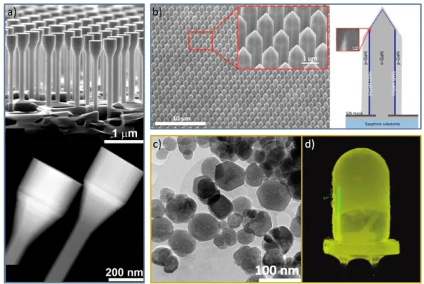
Figure 3 Alternative structures to reduce CMs. (a) Electron microscopy image of InGaN/GaN nanorods with axial QWs (bright strips), fabricated by top down methods. Reprinted with permission from Ref. [55]. Copyright Optical Society of America 2011. (b) Electron microscopy image and schematics of InGaN/GaN nanorods with radial QWs, fabricated by bottom-up method. Reprinted with permission from Ref. [62]. Copyright American Chemical Society 2014. c) Transmission electron microscopy image of YAG:Ce single-nanocrystals obtained by solvothermal method. Reprinted with permission from Ref. [84]. Copyright Royal Society of Chemistry 2018. d) Photograph of a YAG:Ce nanocrystals encapsulated in epoxy, excited at 460 nm. Reprinted with permission from Ref. [85]. Copyright American Chemical Society 2009.
4.2 Partial or Entire Substitutions of Critical Materials: Alternative Materials for
pc-wLEDs
23
If the removal of InGaN quantum wells in GaN-based blue LEDs is technically possible, the associated reduction of IQE and eventually of luminous efficacy would compensate the decrease in the manufacturing impact through the substitution of In. Instead, InGaN-GaN materials should be partially or entirely substituted, by suitable direct wide band gap p- and n-type semiconductors based on abundant and non-toxic elements that could be manufactured with low impact synthesis methods, as shown in Figure 4.
The first materials used for blue LEDs were silicon carbides (SiC), with an emission around 455 nm [86,87]. Due to its indirect bandgap, the EQE is low, only reaching 1% in most recent SiC blue LEDs [88]. It would take a scientific breakthrough to achieve a SiC-based commercial blue in lighting applications.
Then, ZnO is an abundant material possessing excellent properties for blue and UV electroluminescence owing to its direct wide band gap energy of 3.37 eV and its large exciton binding energy of 60 meV at room temperature. For these reasons, homojunctions based on n- and p-type doped ZnO were extensively studied. Most notably, Tsukazaki et al. presented a blue and green light emitting diode with a strong rectifying behavior, based on ZnO layers deposited by molecular beam epitaxy [89]. Nevertheless, other ZnO-based LEDs have been scarcely shown in the literature in the last fifteen years. Indeed, the p-type doping of ZnO is experimentally non-reproducible, and its instability has been attributed to a self-compensation mechanism multiplying the density of shallow donors and favoring the formation of n-type doped ZnO [90,91].
Accordingly, ZnO has been associated with other p-type semiconductors to form heterojunctions and create LEDs [92,93]. The main technological challenge resides in the formation of a defect-free heteroepitaxy, the interface at the atomic scale between ZnO and a suitable p-type semiconductor having a compatible crystal structure. Indeed, the recombination of electrons and holes forming a blue photon occurs precisely at this axial junction. To prevent the formation of interface defects, a general strategy has been to grow an array of ZnO nanowires instead of a thin film, onto the p-type semiconductor. Many publication have recently been devoted to efficient blue LEDs based on n-type doped ZnO nanowires
24
deposited on p-type doped GaN (Figure 4a), producing an emission centered in the range of 397 to 430 nm with a low turn-on forward bias voltage of about 3 V, yet the IQE is not reported [94–97]. Moreover, the growth of a ZnO layer onto GaN nanowires and vice versa has been performed [98–100], which would allow radial junctions increasing the emitting surface as compared to axial junctions.
Additionally, ZnO nanowires have been deposited on other p-type materials such as p-SiC (Figure 4b) [101,102], p-Si [103], or p-polymers [104,105], forming CM-free LEDs yet emitting mostly a broad emission spectrum centered around 520, 535, and 600 nm, respectively, which is less relevant for pc-wLED. Blue emitting CM-free LEDs based on n-type doped ZnO nanowires deposited on p-NiO [106] and p-CuAlO2 [107] were reported, but operating at the high voltage of 18 and 15 V, respectively. Interestingly, it should be point out that ZnO nanowires can be deposited by various physical and chemical methods [108], including low-temperature and low-cost chemical synthesis such as electrodeposition and chemical bath deposition. This opens perspectives towards LED devices with a lower embodied energy [109], also promoting the development of inorganic flexible LEDs, where the use of low-temperature deposition techniques can be achieved on otherwise thermally unstable polymers [110].
25
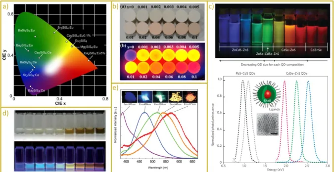
Figure 4 a) Schematics and scanning electron microscopy images of n-ZnO nanorods grown on p-GaN with a hole array-patterned mask layer, and corresponding photomicrograph of the electroluminescent light emission. Reprinted with permission from Ref. [109]. Copyright American Institute of Physics 2016. b) Schematic of n-ZnO nanorods / p–SiC heterojunction LED. Reprinted with permission from Ref. [101]. Copyright Elsevier 2013. c) Electroluminescence spectrum of solution-processed CdS/ZnS based QD-LED measured at the bias of 5.5 V, and corresponding photomicrographs. Reprinted with permission from Ref. [111]. Copyright American Chemical Society 2007. d) Schematic, energy level diagram and normalized photo and electroluminescence of a layered QD-LED device, based on ZnSe/ZnS core/shell QDs. Reprinted with permission from Ref. [112]. Copyright Royal Society of Chemistry 2015. e) Schematic and electroluminescence of a perovskite LED. Reprinted with permission from Ref. [113]. Copyright Nature Publishing 2018.
LEDs based on quantum-dots (QDs) that are nano-sized semiconducting materials with quantum confinement [114] have also undergone significant development in the last decade [115]. Indeed, the whole visible spectrum can be achieved with QDs based on cadmium sulfide (CdS), surrounded by zinc sulfide (ZnS) shell to increase the IQE [111,116,117]. An example of blue emitting CdS/ZnS-based
26
LED is shown in Figure 4c. As in the case of nanowires or nanorods, their nanometric size is compatible with their integration into flexible electronics [118]. Their main drawback is the presence of toxic Cd, together with their sharp drop in the IQE for blue emission. Nevertheless, a Cd- and CM-free LED based on ZnSe/ZnS core/shell QDs shown in Figure 4d produced a emission at 430 nm, with a EQE of 7.83% and a threshold voltage of 8V [112], allowing optimistic perspectives on the implementation of QDs in lighting devices.
Finally, we should mention emerging hybrid halide perovskite-based LEDs that recently showed an interesting EQE of 20% in the green (Figure 4e) [113] and red [119] parts of the electromagnetic spectrum. This emerging class of materials can be deposited by low-temperature solution processes, but contains toxic lead (Pb) in their structure.
4.2.2. Alternative Phosphors
The most relevant partial substitution path leading to efficient phosphors consists in using a CM-free matrix hosting a RE element as dopant and thus removing Y as the majority CM in YAG:Ce phosphors. The dopant RE element, used in very little amount to ensure a high QYP, is either Ce or most frequently Eu, due to their strong emission in the visible part of the electromagnetic spectrum [120]. Thus, several families of matrix suitable to host Ce and Eu for pc-wLED application have extensively been studied [120–123], such as sulfides, oxynitrides, nitrides, and silicates. In each family, CM-free phosphors can be found, by discarding frequent CMs such as Ga, Y, but also barium (Ba), gadolinium (Ga) and lanthanum (La).
27
Figure 5 a) Emission color of Eu- and Ce-doped silicon sulfide matrix. Reprinted with permission from Ref. [124]. Copyright MDPI 2010. b) Photograph of CaZn1-xMnx under daylight and under excitation at
254 nm, with varying Mn content. Reprinted with permission from Ref. [125]. Copyright American Chemical Society 2015. c) Photograph of the photoluminescence of Cd-based QDs of various size and composition, under UV excitation. Schematic and transmission electron microscopy image of core-shell QDs (scale bar is 1.5 nm), and photoluminescence spectra of such QDs. Reprinted with permission from Ref. [117]. Copyright Nature Publishing 2013. d) Photographs of carbon dots under white and UV light. Reprinted with permission from Ref. [126]. Copyright Wiley & Sons 2007. e) Photoluminescence spectra and photographs of BCNO phosphors. Reprinted with permission from Ref. [127]. Copyright Wiley & Sons 2008.
Eu-doped sulfide phosphors have been developed for several decades, and are suitable for warm-light emissions [124]. CM-free compositions can be found, such as calcium sulfide, calcium silicon sulfide, calcium zinc oxysulfide, as shown in Figure 5a. The main drawback of this family is their lack of chemical stability, being easily deteriorated by humidity and gases. More stable Eu- and Ce-doped oxynitrides and nitrides have extensively been developed in the last two decades [128], with QYP reaching 80% [120], leading to their integration into commercial fluorescent lamps. Their composition includes abundant elements, such as silicon, aluminium nitrogen and oxygen, associated either with lithium, calcium, strontium, barium, or lanthanum elements, from the least critical to the most critical
28
chemical element. Finally, one should mention the case of abundant-material-based amorphous matrix such as borate, phosphate, and aluminosilicate, hosting RE elements [129–131]. Nevertheless they often require an excitation in the ultra-violet part of the electromagnetic spectrum and their efficiency is lower than previously described phosphors.
The challenge of synthesizing efficient CM-free phosphors is related to the incomparable efficiency of Ce and Eu to down-convert blue or near ultra-violet emissions into suitable visible spectra for pc-wLEDs, except the case of manganese (Mn). The latter is an abundant element and an efficient red-emitter, as shown in Figure 5b. Thus, it is often used in combination with conventional RE-based phosphor, although harder to be excited and subject to saturation [125,132,133]. Hence, white (or green if combined with Mn) emitting CM-free materials are key to be developed.
Conversion layers based on semiconducting QDs have also received attention in the last decade, due to their QYP above 70%. By showing a narrow emission leading to pure colors (Figure 5c), such particles have been implemented in commercial flat panel displays [115]. Accordingly, they may be implemented as a supplement to traditional phosphors (or their substitutions) for allowing a fine adjustment of CRI and CCT. Nevertheless, the most efficient QDs are based on toxic Cd, lack thermal stability with a threefold decrease in QYP from room temperature to 200°C, and suffer from reabsorption decreasing the overall CE [123]. Finally, Cd-free alternatives contains CMs, such as red emitting InGaP/ZnS core/shell QDs.
Carbon dots, nano-sized carbonaceous clusters named in reference to the previously described semiconducting QDs, have attracted a lot of attention as they are mainly based on carbon, the most iconic abundant element, and synthesized by soft chemistry using low temperature. These non-toxic particles exhibit tunable luminescence [134,135] as shown in Figure 5d, yet their QYp and thermal stability do not meet the commercial phosphor requirements [136]. Carbon is also involved in the photoluminescence properties of defect-related materials. This diverse class of phosphor materials synthesized by low-temperature chemical methods comprises abundant matrix such as alumina [137], boron carbon oxynitrides (BCNO) (Figure 5e) [127], or aluminium borate [83,138], where the
29
luminescence properties of carbon molecules or clusters are enhanced and protected by a rigid inorganic matrix, allowing optimistic perspectives toward CM-free phosphors.
Finally, the emerging hybrid halide perovskites also possess strong and tunable photoluminescent emission, but their poor stability is prohibitive for an implementation in pc-LED [139], in addition to their toxicity from the lead (Pb) in their structure.
We have shown here the role of each CM included in pc-wLED, and the alternative technologies currently developed for reducing or even replacing them partially or entirely. Nevertheless, the determination of reliable data on the economic viability of these alternative technologies requires to define the time and geographic frame, as well as the related cost increase. This depends on fluctuating raw material prices, past, present, and future industrial investments leading to mass production, and regular fluctuations in product supply and demand. Finally, the benefits originating from each of the substitution of CMs in these alternative technologies would require state-of-the-art criticality analysis [140], together with state-of-the-art life cycle assessments.
5. CONSUMERS INTEREST FOR REMOVAL OF CRITICAL MATERIALS IN
PC-wLEDS
The implementation of new materials substituting critical or polluting ones can cause an extra production cost that is difficult to estimate. The reverse reasoning raises the question of what price a consumer would be willing to pay for less material-intensive products. This question is key, not only to investigate alternative market opportunities, but also to assess consumer awareness of the effect of mineral resource consumption, which is ultimately required to build a global mineral resource governance [141]. According to a standard economic approach, consumer preferences focus on the product attributes that have a direct effect on its use or its consumption. Then, an ecological performance that would have no effect on these attributes should not induce a particular valuation. However, many empirical studies have shown that the usual view of rationality as a strictly welfare-maximizing behavior should be replaced by a wider notion of rationality, where the welfare of others and the quality of the
30
environment matter. Individuals not only care about their own interest, but also take into account the well-being of others either directly or indirectly through the consideration of the environment. Such behaviors rely on pro-social preferences where the well-being of others influences one's well-being. There is a lot of experimental evidences of such preferences in many sectors including organic food [142,143], recycled products [144], or remanufactured devices [145].
Instead of pricing the substitute solution (that should be done for each substitute), we chose to estimate the economic value that a consumer could place in a CM free pc-wLED. Even if the cost of the substitute solution could be ultimately lower than the traditional wLED, the consumer preference about such environmentally friendly products must be analyzed in order to estimate the market opportunities for their development. One possible way to measure the economic value for CM free pc-wLED is achieved through the willingness to pay (WTP) defined as the maximum price one would be willing to pay under normal market conditions for a good or service or a specific product feature. When it is not possible to deduce the WTPs from direct observation of buying behavior on the markets, it is often possible to mobilize other methods. For this research, we conducted an experiment with consumers based on the choice experiment (CE) methodology [146]. This discrete choice methodology provides the advantage to simultaneously vary several attributes of a product and to estimate the marginal rates of substitution between these attributes, and especially the WTP for specified characteristics. It provides great flexibility in the sense that many different scenarios can be presented in a single study, as in the case of a store where consumers have to choose between different wLEDs. In order to define our exploration of the relevant attributes of wLED, we carried out focus groups in order to investigate consumers’ understanding and perception of wLED products, but also their production processes. While participants in these focus groups were relatively well informed about the impacts of using CMs in general, it is noteworthy that they were particularly surprised to learn that wLED contain such materials. These focus groups mainly showed that the type of light (warm, cold or neutral), the price and the electrical consumption of the wLED are the most important attributes. According to our main research objectives, we added two other attributes: i) production impact on the environment (a composite
31
indicator which take into account carbon emission, waste treatment, energy consumption, land use and contamination for the production of the wLED), and ii) the use or not of CMs (presented through their three dimensions: environmental impact, dependence on producer countries and working condition). All other characteristics of products were kept constant. Including conjointly these two attributes in the study is intended to allow us to estimate the specific impact of the presence of CMs beyond the general concern for environmental protection.
By taking into account the technical specificities of wLEDs currently on the market and their selling conditions, we determined 2-4 levels of specification for the five attributes of our CE. Table 2 displays the levels of the five attributes defining the wLED offered during the experiment.
Table 2
Attributes and their different levels of wLEDs in the CE.
Attributes Level 1 Level 2 Level 3 Level 4
Color temperature Warm Neutral Cold -
Critical Material With Without - -
Electrical
consumption 5 kWh/year kWh/year 10 kWh/year 15 -
Production impact Low Medium High -
Unit price €2 €5 €10 €15
The combination of all attributes and levels would result in 2 × 3 × 4 = 216 different wLED profiles, which would be impractical to present as a whole to the respondents. To reduce the number of choice sets while maintaining statistical efficiency, we used a D-efficient design generated by software Ngene© (see www.choice-metrics.com). The final number of choice sets was 108 grouped in four blocks of 36 wLED profiles.
The scenario proposed to the participants is that of an in-store purchase of a wLED for their living room. The choice task is intended to resemble actual purchase decisions with the inclusion of a ‘do not buy’ option. This feature ensured that subjects were never forced to purchase a wLED. As in a real shopping situation, they had the possibility of not purchasing any wLED if none of the alternatives suited
32
them in a choice set. Consumers were asked to choose between three wLED and ‘do not buy’ option. In total, they made 9 different choices displayed on 9 different cards as shown in Figure 6.
Figure 6 Example of choice task used in the CE as presented to the participants
The experiments were run between the 8th and 16th of July 2019, in Grenoble. The session started with a presentation of LED attributes, on which participants must have based their choices. This introduction lasted about 20 minutes, then the CE began. There were 297 participants for this study, 12 of them were excluded because they declared to use only two attributes to make a choice. Participants were aged between 20 and 65, and the mean age was 40 years-old. There were 66 % of female and 34 % of male, and about 40 % were employee. Compared to the general French population, female and employee are over-represented in our sample.
Consumer preferences were elicited on the basis of the random utility model (RUM) [147]. This general estimation framework provides the opportunity to estimate the effects of product attributes and to compute willingness to pay indicators. Our data were analyzed with a nested logit model [148]. which includes the branch of « do not by a wLED » and the branch grouping the three wLED alternatives. The widely adopted paradigm of utility maximization provides a link by which choice probabilities can be estimated as a function of the characteristics of the wLED. The session ended with a sociodemographic questionnaire. Participants were also asked about their preferred attributes for purchasing wLED light bulbs.
The final model representing utility 𝑈 of person 𝑛 from choosing alternative 𝑗 in the choice scenario 𝑡 is given by:
33
𝑈 , , = 𝑤𝐿𝐸𝐷 + 𝛼 × 𝑝𝑟𝑖𝑐𝑒, , , + 𝛽 × 𝑋 , , , + 𝜖 , ,
where 𝑤𝐿𝐸𝐷 is the parameter representing the preference to buy a wLED instead of choosing not to buy option. The 𝑝𝑟𝑖𝑐𝑒, , , is a price attribute (€5, €10 and €15 compared to €2) and 𝛼 is the corresponding parameter to estimate, 𝑋 , , , is a vector of no price attributes and 𝛽 is the corresponding parameter vector, finally 𝜖 , , is the random part of utility assimilated to the error term of estimation. We separated the effect of each price level to take into account no linear preference for price. The color attribute was replaced by dummy variable that was equal to 1 if the color of wLED offering corresponds to consumer 𝑛 preferred color. In fact, 47% consumers prefer warm color for living room, 11 % cold color and 42 % neutral color, respectively.
Table 3 shows the results of estimated parameters 𝑤𝐿𝐸𝐷, 𝛼 and 𝛽: the marginal impact of the different attributes on the probability that a wLED will be chosen compared to a reference wLED. The reference wLED (RefwLED) is characterized by a price of €2, with the color different from preferred color, using CMs and with a high level of production impacts. Since electrical consumption is a cardinal quantity, the impact of an increase of 1 kWh/year on the probability of purchase is directly measured.
34 Table 3
Results of the nested logit regression
Variable Coefficient Standard
Err. Z stat P-value wLED -0.0336 0.007 -4.8 0 Price €5 vs €2 -0.0129 0.073 -0.18 0.86 Price €10 vs €2 -0.4314 0.0783 -5.51 0 Price €15 vs €2 -1.1174 0.1096 -10.19 0 Preferred color 0.8309 0.0713 11.66 0 Without CM 1.2147 0.0894 13.58 0
Medium vs High impact 1.1816 0.0937 12.6 0
Low vs High impact 1.6949 0.1185 14.3 0
Electrical consumption -0.1226 0.0119 -10.29 0
𝝉 (wLED nest) 0.818234 0.0629 CI 95% [0.6949 ;0.9415]
𝝉 (do not buy nest) Constrained to 1
RUM-consistent nested logit regression Number of cases: 2466 Alts per case: 4 Number of obs.: 9864 Wald chi2(11) = 518.31 Log likelihood = -2497.5492 Prob > chi2 = 0.0000
Only €5 price parameter is not significant; it means that there is no difference for consumer to buy a wLED at €2 or to buy it at €5. This indifference between the two low prices is explained by the current high prices of LEDs and level of income of consumers in France. The probability of choosing a wLED decreases by increasing its price (negative coefficients -0.4314 and -1.1174 for respectively €10 and €15 prices). Concerning electrical consumption, a higher consumption implies a lower probability of being chosen. Finally, wLEDs without CM and wLEDs with medium or low environmental impacts have been chosen more frequently, indicating the existence of pro-social preferences.
In order to estimate the market opportunities for the development of CM-free wLED, we determined the marginal WTP that consumers are ready to pay for such product. The marginal WTP are computed as the marginal rate of substitution between the « quantity » expressed by the attributes and the price or more simply as a ratio between parameter of attribute 𝑘 multiplying by −1 and price parameter 𝛼 :