HAL Id: lirmm-00616949
https://hal-lirmm.ccsd.cnrs.fr/lirmm-00616949
Submitted on 14 Sep 2019
HAL is a multi-disciplinary open access
archive for the deposit and dissemination of
sci-entific research documents, whether they are
pub-lished or not. The documents may come from
teaching and research institutions in France or
abroad, or from public or private research centers.
L’archive ouverte pluridisciplinaire HAL, est
destinée au dépôt et à la diffusion de documents
scientifiques de niveau recherche, publiés ou non,
émanant des établissements d’enseignement et de
recherche français ou étrangers, des laboratoires
publics ou privés.
Ultra Compact Non-Volatile Flip-Flop for Low-Power
Digital Circuits Based on Hybrid CMOS/Magnetic
Technology
Gregory Di Pendina, Guillaune Prenat, Khouldoun Torki, Yoann Guillemenet,
Lionel Torres
To cite this version:
Gregory Di Pendina, Guillaune Prenat, Khouldoun Torki, Yoann Guillemenet, Lionel Torres. Ultra
Compact Non-Volatile Flip-Flop for Low-Power Digital Circuits Based on Hybrid CMOS/Magnetic
Technology. PATMOS: Power And Timing Modeling, Optimization and Simulation, Sep 2011, Madrid,
Spain. pp.83-91, �10.1007/978-3-642-24154-3_9�. �lirmm-00616949�
J.L. Ayala et al. (Eds.): PATMOS 2011, LNCS 6951, pp. 83–91, 2011. © Springer-Verlag Berlin Heidelberg 2011
for Low Power Digital Circuits
Based on Hybrid CMOS/Magnetic Technology
Gregory Di Pendina1, Kholdoun Torki1, Guillaume Prenat2,Yoann Guillemenet3, and Lionel Torres3
1
CMP – Circuits Multi-Projets, 46 Avenue Felix Viallet, Grenoble, France {gregory.dipendina,kholdoun.torki}@imag.fr
2
SPINTEC, CEA, CNRS, UJF, INPG; CEA/INAC 17 Rue des Martyrs, 38054 Grenoble Cedex, France
guillaume.prenat@cea.fr
3
University of Montpellier 2 – LIRMM – UMR CNRS 161 Rue ADA, 34 392 Montpellier, Montpellier, France {yoann.guillemenet,lionel.torres}@lirmm.fr
Abstract. Complex systems are mainly integrated in CMOS technology, facing
issues in advanced process nodes, in particular for power consumption and heat dissipation. Magnetic devices such as Magnetic Tunnel Junction (MTJ) have specific features: non-volatility, high cyclability (over 1016) and immunity to radiations. Combined with CMOS devices they offer specific and new features to designs. Indeed, the emerging hybrid CMOS/Magnetic process allows integrating magnetic devices within digital circuits, modifying the current architectures, in order to contribute to solve the CMOS process issues. We present a high performance innovative non-volatile latch integrated into a flip-flop which can operate at high speed. It can be used to design non-volatile logic circuits with ultra low-power consumption and new functionalities such as instant startup. This new flip-flop is integrated as a standard cell in a full Magnetic Process Design Kit (MPDK) allowing full custom and digital design of hybrid CMOS/Magnetic circuits using standard design tools.
Keywords: Non-volatile, Latch, Flip-Flop, Magnetic Tunnel Junction, Low
Power, Full Custom Design, Digital Design, Process Design Kit, Standard Cell.
1 Introduction
For almost 40 years, the development of electronic circuits is evolving according to more or less Moore’s law: speed and density double every 18 months. But in advanced technology nodes, this trend tends to get out of breath. Indeed, due to the small dimensions of the devices and the high speed operations, the power consumption of logic circuits becomes larger and larger, resulting in heat dissipation and reliability issues. Several techniques have been implemented to decrease the power consumption of logic circuits [1] (clock and power gating, dynamic voltage
84 G. Di Pendina et al.
frequency scaling...). Power gating consists in cutting off the power supply of unused blocks of a circuit to reduce the standby power consumption. With volatile memories, this technique requires copying the data into non-volatile or very low leakage memory, resulting in delays and dynamic power consumption. Using a non-volatile flip-flop (NVFF) allows cutting off the power supply without any additional operation and with very low area overhead, allowing an efficient instant on/off policy. In this way it allows the circuit to be stopped and restarted at once on demand with full performance, leading to the concept of “normally off electronics”. This also improves the circuit reliability in particular against power failures. Radiation immunity is a further advantage of this hybrid CMOS/Magnetic technology. In this paper, we present a compact and high performance non-volatile latch integrated into a flip-flop and a full Magnetic Process Design Kit (MPDK) allowing full custom and digital design of hybrid CMOS/Magnetic circuits. The first part deals with the magnetic technology, the second part is dedicated to the description of the non-volatile latch and finally, we present the MPDK embedding the latch into a flip-flop as a standard cell to be used in a conventional CMOS design flow.
2 Technology and Device
2.1 Magnetic Tunnel Junction Using Thermally Assisted Switching Method
A Magnetic Tunnel Junction (MTJ) is a nano-structure basically composed of two ferro-magnetic layers separated by an oxide layer as shown in Fig.1. The magnetization of one of the magnetic layer, called the hard layer, is pinned and acts as a reference, while the magnetization of the second layer, called the soft layer, can be switched by an external magnetic field, or a current. The resistance of the MTJ depends on the relative magnetization of the two layers (Tunnel Magneto-Resistance, TMR): the resistance in the parallel state (RP) is lower than the resistance in the antiparallel state (RAP). These two values typically differ by a factor 2 to 3. The MTJ pillar has typically an elliptical shape. Due to shape anisotropy, the long axis of the ellipse constitutes an easy axis of magnetization. In the absence of external solicitation, the magnetization of the soft layer lies in one direction or the opposite one along this axis. In practice, for memory and logic applications, the magnetization has two stable states, parallel or antiparallel to the hard layer magnetization, with an hysteretic behavior. In this case, the value stored in the MTJ is represented by its magnetic configuration and the associated resistance value. Writing an information in the MTJ consists in orienting the magnetization of the storage layer either parallel or antiparallel to that of the reference layer. In the first MRAM generation [2], this is performed by a pulse of magnetic field generated by a pulse of current flowing in a current line located above or below the MTJ. This approach suffers from selectivity and scalability problems. The Thermally Assisted Switching (TAS) approach relies on the strong dependency of the magnetic properties upon temperature: a pulse of current is first applied throughout the MTJ to heat it above a so-called “blocking” temperature. It can then be easily switched by a low-magnetic field. Subsequently, the heating current is switched off so that the MTJ cools down to ambient temperature. This heating and cooling process only takes about 20ns. It insures an excellent retention of the information in standby for more than 10 years. This technology is being developed by the MRAM manufacturer CROCUS-Technology.
Fig. 1. MTJ Device Principle
2.2 Technology and Post Process of the Hybrid CMOS/Magnetic Process
The hybrid technology presented here has been developed in the framework of a French national project SPIN [3]. The magnetic devices are fabricated at CEA-LETI and CROCUS-Technology, in post-process above the STMicroelectronics 130nm CMOS process. Fig. 2 shows a cross-section of the technology: it integrates the whole standard CMOS process, the magnetic layers with the MTJ itself, top and bottom electrodes plus vias to connect the MTJ to the CMOS layers. An interesting feature of this post process is its full compatibility with any standard CMOS process.
Fig. 2. Hybrid CMOS/Magnetic Process Cross Section
3 Innovative Cell and Tools
3.1 4 Transistor Loadless Non-volatile Cell
An innovative non-volatile SRAM cell, made by Black and Das (B&D), has been proposed in [4]. It has been adapted to the TAS technology in [5] and integrated into a non-volatile flip-flop in [6] and [7]. The SRAM cell has been modified adding two MTJ acting in differential mode: one MTJ is in parallel state while the other is in antiparallel state. Thus, two logic values are coded in the cell: one in the magnetic
86 G. Di Pendina et al.
part and one in the latch itself. They are independent since it is possible to write the magnetic information without affecting the latch and vice-versa. This cell requires 9 transistors instead of 6 in a classical SRAM cell, two of them being dedicated to heating the junction. The B&D can be used as any CMOS latch. A simple pulse of voltage on a so-called “Autozero” (Az) additional transistor allows transferring the value of the MTJ into the latch.
Several years ago, on previous generation processes, the 6 transistor (6T) SRAM were modified by replacing 2 transistors by 2 resistor loads above the 4 remaining transistors in order to improve the density, yielding a 4T SRAM. To operate correctly, the device requires high resistance values to ensure good logic levels and to limit the power consumption. Moreover, the resistance’s area increases with advanced technology nodes compared to transistors area, so that the size of the resistors becomes prohibitive. In addition, the 4T SRAM suffers from intrinsic static power consumption and is sensitive to noise and soft errors because of the high resistance values. To solve these problems, a loadless 4T SRAM cell has been proposed in [8], in which the access transistors are also used as load transistors: when they are “on”, they are connected to the bit lines and allow the access to the SRAM cell for read and write operations. When they are “off”, they are connected to the power supply and maintain the output logic levels “Q” and “Q_” by leakage currents. To operate correctly, the leakage current at “off” state has to be higher in the access transistors than in the latch transistors, to ensure logic levels to be compatible with the technology. This is performed by using low-threshold access transistors and high-threshold latch transistors.
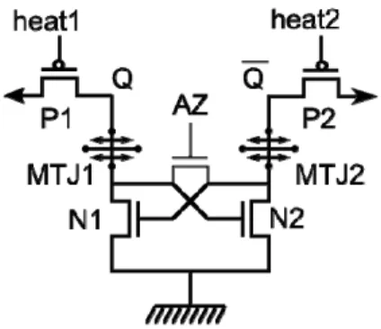
We propose here a new non-volatile cell based on the 4T loadless SRAM. Two MTJ are added in the 4T SRAM cell as illustrated on Fig. 3.
The main innovation of this cell is that it uses the same path to write the MTJs and to read their state. Writing the MTJs is performed in two cycles, with the access transistors connected to vdd: first, one access transistor is activated for example applying a low level on the heat2 control signal. This saturates the N1 transistor. A low level on heat1 control signal allows the generation of the heating current for the MTJ1. The writing magnetic field can then be applied to write to the MTJ. This operation is repeated to write to MTJ2. In standby state, the access transistors are connected to vdd, but in “off” state. To restore the value of the magnetic part into the latch, P1 and P2 are on, connected to the power supply again and an Az pulse is applied: the latch operates as a sense amplifier to read the difference of resistances in the two branches. In non-magnetic operations, data can be read or written directly to the latch. In this case, P1 & P2 are connected to the bit lines and activated at the same time. Since the resistance of the MTJs is comparable to the “on” resistance of the transistors, their presence does not disturb the writing/reading operations. The heating resulting from the current passing through the MTJs is not a problem since no magnetic field is applied at this time.
The main advantage of this approach is that it requires only 5 transistors instead of 9 in the classical TAS B&S cell. Moreover, since the heating current is proportional to the surface of the junction, it decreases very quickly with the technology node. It is possible to use minimum size transistors to generate the heating current from 65nm CMOS technology and below, which means that a SRAM can be made fully non-volatile with a very low area overhead.
Fig. 3. 5 Transistor Loadless Non-volatile Cell
This compact innovative non volatile cell could be used in Magnetic RAM (MRAM) architectures which would enable to reduce the memory area in the design or to increase the storage capability for a given area. However we present below how this cell can be implemented in a flip-flop to make it non volatile. This innovative cell is used as the first latch of a flip-flop, while the second latch is a classical 6T SRAM.
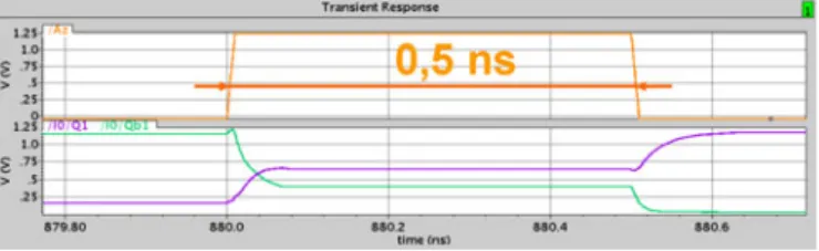
This cell can be used as a classical register for high-speed operation. It also offers the possibility to backup its content into the magnetic part at any time and to restore it with an Az pulse shorter than 1ns as illustrated in Fig. 4, to restart the logic on a known state.
Fig. 4. Ultra Compact Non-volatile Flip-Flop
The total write time of this NVFF is typically around 40ns, driven by the heating/cooling rates, themselves depending on the materials. This allows a high frequency and low-power backup of the data in the non-volatile part in comparison with Flash for example. For applications which do not require a very high operation speed, it is even possible to write the MTJ at each clock cycle, resulting in a fully non-volatile logic circuit. This cell can be used for example to ease the power gating technique: in operation, the cell acts as a standard latch. When the block has to be deactivated, the
88 G. Di Pendina et al.
active data of the latch can be copied in the magnetic part, and the power supply totally switched off using ultra low leakage transistors. Thus, the standby consumption is lower than the technics consisting in lowering the voltage for SRAM data retention. When the block has to be used again, a simple Az pulse allows for immediate recovery of the data, to retrieve the state of the block.
Fig. 5. Flip-flop Reading Operation Simulation with TAS method
3.2 Full Custom Flow and Tools
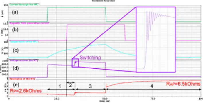
Concerning the front-end, an electrical model of the MTJ has been developed [9]. The result is a dynamic library which can be loaded by an electrical simulator (for instance Spectre). The use of this model is very similar to that of the bsim model of the transistor: the model is a generic representation of the MTJ, which contains a given number of parameters. Some of these parameters are chosen independently for each instance. It is typically the case for geometrical parameters (size, shape...). They can be chosen by the designer when instantiating the device, according to the post process capabilities. The other parameters are linked to the technology and cannot be modified by the designer. They are provided by the manufacturer in a corner file. This compact model enables one to run an electrical simulation of a design including both standard CMOS devices such as transistors, resistors, capacitors and so on, and the MTJ with its specific signals. A symbol view is available to design a full custom circuit using MTJs. In Fig. 5, (a) is the heating control signal, (b) is the signal to control the generation of the magnetic field, (c) represents the temperature, (d) the voltage across the MTJ and (e) its resistance. During the period (1), a pulse of current is applied to the MTJ, resulting in a temperature increase. Then, a magnetic field is applied. After a delay (2) corresponding to the intrinsic switching duration, the resistance changes, as a consequence of the soft layer magnetization switching whose dynamic behavior is detailed in the inset. Then (3) is the end of the heating phase and (4) the cooling phase during which the temperature returns to the standby value. Fig. 5 (e) clearly shows the effect of temperature and voltage on the electrical resistance.
Concerning the back-end design flow, all necessary technology files have been developed and implemented in the design kit: specific layers have been added to insert the MTJs coupled with their connections. This is fully integrated with CMOS layers in the Cadence Layer Selection Window (LSW). A parameterized cell (PCell) has been developed to ease the MTJ design and to enable interactive parameter modifications when running the simulations and adjusting the full custom design. Regarding the verification, all MTJ’s specific design rules have been implemented in the Design Rule Checks (DRC) with 2 different switches, offering the possibility to run the DRC either on both CMOS and magnetic layers or on the magnetic layers
only. This gives the designers some flexibility. A full extraction is also possible with this design kit which enables one to run Layout Versus Schematic (LVS) checks on the entire design, including magnetic tunnel junctions. As a consequence, a netlist including all devices and parasitics can be extracted from the layout for post layout simulations and validation before manufacturing.
Fig. 6. MTJ Writing Operation Simulation with TAS method
3.3 Digital Flow and Tools
A complex digital architecture can be made of standard volatile CMOS blocks and non-volatile CMOS/Magnetic blocks. Each of them needs to be described in a Hardware Description Language (HDL) before the synthesis. In order to be able to run digital simulation for advanced and complex designs, a full Verilog description of the NVFF has been developed. It takes into account the behavior and also the timing checks for the MTJ’s heating duration, writing and reading. Indeed, the TAS method has very strict intrinsic timing constraints which need to be taken into account to ensure the simulation reflects the real MTJ behavior, as we have in full custom simulations using the compact model.
To design non volatile blocks using the innovative flip-flop standard cell described above, the synthesis uses a specific library containing only registers made of CMOS and MTJs. The connections between all the magnetic signals such as Heat1, Heat2 and Az are defined in the HDL description where all these signals need to be declared and interconnected to manage the MTJ writing and reading. As a consequence, the netlist extracted from the synthesis includes the NVFF and both connections of CMOS signals (D, Clk, Q, Rst, Set …) and magnetic signals. The abstract view of the NVFF is given in order to place and route a full block composed of standard cells, using standard tools. Once the place and route job is completed, only the write signal paths need to be placed over all the rows composed of non volatile flip-flops and connected to current generators to generate the switching field. Since these specific cells can be neither flipped nor mirrored because of the importance of the write field direction, MTJs are placed only every 2 rows. To complete final simulations, an SDF file including the NVFF internal timings can be extracted from the placed and routed layout to back annotate the netlist to run more accurate simulations. Fig. 6 shows the layout of a digital filter described in HDL format, simulated with Mentor Graphics /
90 G. Di Pendina et al.
Modelsim, synthesized under Synopsys / Design Compiler, placed and routed with Cadence / Encounter. This filter includes about 1100 standard cells in which about 290 are non volatile flip-flops described above.
Fig. 7. Automatically Placed and Routed Circuit using Non-volatile Flip-Flop Standard Cell
4 Conclusion
Non-volatile technologies and in particular the CMOS/Magnetic are more and more considered as a way to circumvent the limits of advanced CMOS circuits, combined with existing design techniques or technologies. This requires evaluating the use of these new devices in complex systems, and probably adapting the existing techniques and architectures correspondingly. Such studies can only be carried out using tools that integrate these devices in standard design suites. The proposed full MPDK has been developed and used to realize a demonstrator which is currently under fabrication within the SPIN research project. This design kit is compatible with design suites supported by most of the foundries and can be easily improved with the evolution of the technology. It could be adapted to fit accurate characterization results and made available for any designer interested in the design of hybrid Magnetic/CMOS circuits.
References
1. Hu, Z., Buyuktosunoglu, A., Srinivasan, V., Zyuban, V., Jacobson, H., Bose, P.: Microarc-hitectural techniques for power gating of execution units. In: Proceedings of International Symposiumon Low Power Electronics and Design (ISLPED) (August 2004)
2. Andre, T.W., Nahas, J.J., Subramanian, C.K., Garni, B.J., Lin, H.S., Omair, A., Martino, W.L.: A 4-mb 0.18-μm 1t-1mtj toggle mram with balanced three input sensing scheme and locally mirrored unidirectional write drivers. IEEE Journal of Solid State Circuits 23(1), 301–309 (2005)
3. http://www.lirmm.fr/SPIN
4. Black Jr., W.C., Das, B.: Programmable logic using giant-magneto-resistance and spinde-pendent tunneling devices. J. Appl. Phys. 87(9), 6674–6679 (2000)
5. Guillemenet, Y., Torres, L., Sassatelli, G.: A Non-Volatile Run-Time FPGA structures us-ing Thermally Assisted Switchus-ing MRAMs. Journal IET Computers and Digital Tech-niques 4(3), 211–226 (2010), doi:10.1049/iet-cdt.2009.0019
6. Lakys, Y., Zhao, W., Klein, J.-O., Chappert, C.: Low power, High Reliability Magnetic Flip-Flop. Electronics Letters 46(22), 1493, 2 pages (2010)
7. Sakimura, N., Sugibayashi, T., Nebashi, R., Kasai, N.: Nonvolatile Magnetic Flip-Flop for Standby-Power-Free SoCs. IEEE Journal of Solid State Circuits 44(8) (August 2009) 8. Noda, K., Matsui, K., Takeda, K., Nakamura, N.: A loadless CMOS four-transistor SRAM
cell in a 0.18-μm logic technology. IEEE Transactions on Electron Devices 48(12), 2851–2855 (2001), doi:10.1109/16.974716
9. ElBaraji, M., Javerliac, V., Guo, W., Prenat, G., Dieny, B.: Dynamic compact model of thermally assisted switching magnetic tunnel junctions. Journal of Applied Physics 106(12), 123906 (2009)