Bipolar Cascade Lasers
by
Steven G. Patterson
B.S. University of Cincinnati (1993)
S.M. Massachusetts Institute of Technology (1995)
Submitted to the
Department of Electrical Engineering and Computer Science
In partial fulfillment of the requirements for the degree of
Doctor of Philosophy
at the
MASSACHUSETTS INSTITUTE of TECHNOLOGY
SEPTEMBER 2000
@ 2000 Massachusetts Institute of Technology
All rights reserved
MASSACHUSETTS INSTITUTE OF TECHNOLOGY
OCT 2 3 2000
LIBRARIES
r
Department of Electrical Engineering and Computer Science July 31, 2000
Rajeev J. Ram
Srofessor of Electrical Engineering
Thesis Supervisor
Accepted by
ArtlZr C. Smith Chairman, Department Committee on Graduate Students Autho
Certified by 'I 1
/
'I
Bipolar Cascade Lasers
bySteven G. Patterson
Submitted to the Department of Electrical Engineering and Computer Science on August 4, 2000 in Partial Fulfillment of the
Requirements for the Degree of Doctor of Philosophy in Electrical Engineering
ABSTRACT
This thesis addresses issues of the design and modeling of the Bipolar Cascade Laser (BCL), a new type of quantum well laser. BCLs consist of multiple single stage lasers electrically coupled via tunnel junctions. The BCL ideally operates by having each injected electron participate in a recombination event in the topmost active region, then tunnel from the valence band of the first active region into the conduction band of the next active region, participate in another recombination event, and so on through each stage of the cascade. As each electron may produce more than one photon the quantum efficiency of the device can, in theory, exceed 100%. This work resulted in the first room temperature, continuous-wave operation of a BCL, with a record 99.3% differential slope efficiency. The device was fully characterized and modeled to include light output and voltage versus current bias, modulation response and thermal properties. A new single-mode bipolar cascade laser, the bipolar cascade antiresonant reflecting optical waveguide laser, was proposed and modeled.
Thesis Supervisor: Rajeev J. Ram
Acknowledgements
The graduate experience varies greatly amongst students for a variety of reasons, not the least of which is one's faculty advisor. In this regard I have been most fortunate. Rajeev was kind enough to take me on as a student late in my graduate career, provided tremendous guidance throughout the course of this work, is truly gifted in his amazing physical insight which he readily shares, has always seemed to remember that graduate school is also about educating students and, perhaps most importantly, supported me when others might have (and did) run for cover.
I'd like to thank my thesis committee, Terry Orlando and Shaoul Ezekiel, for reading the thesis and making numerous helpful comments. Thanks to Terry for also
attempting to provide valuable help at a more difficult time during this thesis work. My most sincere appreciation goes to the members of my research group. I'd like to thank Matthew for his sense of humor, for always being supportive, for always having something positive to say, for getting everything together the day of my defense, and for never turning me away whenever I needed a friendly ear. Erwin always seemed to have something nice to say about everyone, even me, and provided entertaining and lively conversation about women, dating and many other aspects of life. Erwin deserves special mention for daring to be different, particularly in an institution that (despite its remonstrations to the contrary) admires only homogeneity in thought and action. Harry generated plenty of laughter and good will through his boyish enthusiasm and charm, was always eager to help out even without being asked, saved me endless hours of mindless drudgery through his mastery of Matlab and Labview, and often reminded me that engineering can still be fun. Kevin was a breath of fresh air to the group bringing in an enthusiasm for things outside the lab, filling me in on the many aspects of life in Cambridge, Boston and at MIT. Thanks also to Kevin for tolerating the mini-music (especially the country stuff), oh and of course, for being the only really normal guy in the group. My first impressions of Margaret (a.k.a. Bob) were of an extremely warm and sweet person and these initial impressions have only grown stronger with time. Her genuine smile and easy going manner, not to mention her baking, have made her presence in and about the lab a delight. Farhan's mastery of condensed matter physics, his willingness to share his knowledge of the same and our common ground of prior military service made for many interesting and fruitful interactions. A special thanks to Holger for maintaining the soft spoken and humble manner with which he arrived, particularly in an institution that seems to honor pomposity and arrogance above all else. Peter is relatively new to the group and the unfortunate paucity of available time has not permitted a closer acquaintance but his friendly manner and insightful questions have made him a welcome addition to the group.
I have been equally blessed to have acquired so many wonderful friends over the years. Dave, as different as we may be, has remained a true friend over the years, providing countless hours of conversation and a tireless patience with my miscellaneous ramblings. Thanks also, in no small measure, for the splendid bottle of scotch. Amy has helped me better understand the other half, always seemed to be in the office during her MIT years whenever I needed a quick chat or to share a cup of coffee, and embraces life in a manner which I find truly inspiring. Enrique, the salsa king of Boston, livened my days at MIT with many a trip to the Muddy, by continuing to attempt to teach me to
dance even when I was clearly a danger to myself and those around me, and by just being what is best described as a buddy. Mark has helped me prove that there is indeed hope for the world if a highly intelligent, double majoring, avowed liberal, Rhodes Scholar, professor of physics could provide such enduring friendship to such an uncredentialed, barely made it to college, Neanderthal former Ranger-type. Glenn I met as an undergrad while interning and it is through his encouragement that I realized that MIT was not beyond my grasp. He has remained a dear friend in spite of the large physical distance separating us over the years. Reggie is the sort of friend whom, no matter the length of time since we last spoke, immediately allows me to feel at home, welcome and reconnected. Bob and Kirstin have been supportive beyond mere description in words and no amount of space is adequate to do justice to the contributions they've made over the years to the betterment of my life. Felicia has always been a source of inspiration, encouraging me long ago to take the road which brought to where I am today. It would be hard to imagine a better sister. My parents taught me long ago about the importance of self-reliance and that hard work eventually does indeed pay off.
Finally, I'd like to express my continuing admiration for the men, past, present and future, of the Ranger Regiment. It is there that I learned almost everything of intrinsic value in life. The rest has been mere technical details.
Contents
1 Introduction 15
1.0 Introduction 15
1.1 Cascade lasers 16
1.2 A brief history of cascade lasers 22
1.3 An alternative: The gain-lever laser 23
1.3.1 Achieving RF gain by other means 25
1.4 Dissertation overview 25
2 Semiconductor Tunnel Junctions 29
2.0 Introduction 29
2.1 Tunnel junctions 30
2.2 Tunnel junction modeling 32
2.3 Materials considerations for semiconductor tunnel junctions 45
3 Bipolar cascade lasers 59
3.0 Overview 59
3.1 Cascade laser theory 59
3.2 Materials growth of semiconductor lasers 66
3.2.1 Single stage lasers 66
3.2.2 Active region growth 71
3.2.3 Growth consideration at interfaces 72
3.2.4 BCL growth and design 73
3.3 BCL Characterization 75
3.4 Thermal modeling of the bipolar cascade laser 79
3.5 Antiguiding and other non-ideal behavior in BCLs 90 3.6 Modulation properties of the bipolar cascade laser 93
3.7 The second generation bipolar cascade laser 95
4 Antiresonant reflecting optical waveguide lasers 105
4.0 Introduction 105
4.1 The optical fiber coupling problem 106
4.2 The antiresonant reflecting optical waveguide bipolar cascade laser 111
5 Summary and directions for further work 125
5.0 Introduction 125
5.1 Summary 125
5.2 Directions for future work 128
A Mathematical description of the tunnel junction 135
B Laser physics basics 143
D Single stage ARROW laser design 155
List of Figures:
1-1 A unipolar cascade laser...17
1-2 The type-Il bipolar cascade laser...17
1-3 Conventional QW laser band diagram...18
1-4 The circuit equivalent of Fig. 1-3...18
1-5 A bipolar cascade laser...19
1-6 The circuit equivalent of Fig. 1-5...20
1-7 The proof-of-concept experimental set-up used in generating the data of Fig. 17b....21
1-8 The gain lever laser... 24
2-1 The unbiased p-n tunnel junction...30
2-2 The tunnel diode under forward bias...31
2-3 The tunnel junction biased to the point where tunneling current no longer flows...31
2-4 The tunnel junction in reverse bias...32
2-5 The tunneling potential used to calculate the tunneling probability...34
2-6 Components of momentum perpendicular to the direction of tunneling result in an increase in the effective bandgap energy for interband tunneling...35
2-7 Calculated and measured tunneling currents...39
2-8 Tunneling current versus applied voltage for a 20 gm wide by 500 gm long device doped 2x10'9 cm-3 on the n-side...40
2-9 The forward tunelling currents of Fig. 2-8...41
2-10 The tunneling current versus voltage for 20 gm by 500 pim device with In mole fractions varying from 0-15% in 5% increments...42
2-11 The junction resistance versus p-type doping density of a 20 jm by 500 jm tunnel junction doped to 2x10 19 cm-3 on the n-side of the junction over a bias range of 20-50 m A ... . . ..4 3 2-12 The differential resistance for the device of Fig. 2-11...43
2-13 The resistance of a 20 jm by 500 jm tunnel junction versus acceptor concentration doped 2x10'9 on the n-side of the junction for GaAs and Ino.15GaO.85As devices...44 2-14 The differential resistance versus acceptor concentration for the device of Fig. 2-13. ... 4 4 2-15 The differential resistance versus acceptor concentration for the device of Fig. 2-13. ... . . 4 5
2-16 Peak achieved doping densities versus substrate temperature for Si and Be in GaAs.
... 4
2-17 Secondary ion mass spectroscopy measurement of a GaAs tunnel junction embedded in a two stage bipolar cascade laser...51
2-18 A tunnel junction containing a large density of deep level impurities...53
2-19 The effect of the deep level states upon the current versus voltage characteristics of the ideal tunnel junction...53
2-20 Bipolar cascade laser at equilibrium...55
3-1 The carrier density versus bias current in a 20 gm by 500 gm two-stage bipolar cascade laser... ... ... 64
3-2 The voltage versus bias current of the device of Fig. 3-1...65
3-3 The normalized increase in Vth/Vtho, IID/rIDo, Ith/Itho versus the number of gain stages. ... . . . ..6 6 3-4 The test structure used to study the effect of substrate temperature upon the optical qualities of a single stage edge-emitting laser...67
3-5 The photoluminescence intensity versus energy of the three test structures used to determine acceptable substrate temperatures for growth of the bipolar cascade laser...68
3-6 The light power versus bias current for a an aluminum free single stage edge emitting lasers. The continuous wave threshold current density is 330 A/cm ... 70
3-7 The device structure for the first bipolar cascade laser...74
3-8 The-light power versus bias current of the first room temperature, continuous wave bipolar cascade laser...76
3-9 The voltage versus current of the device of Fig 8...77
3-10 The bias current versus emission wavelength for a two-tone BCL...79
3-11 The light power versus bias current for a 20 gm wide, 300 gm long device...80
3-12 The definition of T0... . . . .. . . ...81
3-13 The differential slope efficiency versus heat sink temperature for the device of Fig. 3-1 1 ... . . 83
3-14 The definition of T1... .. . . .. . . 84
3-15 The differential slope efficiency versus heat sink temperature for the device of Fig. 3 -1 1 ... . . 8 5 3-16 The surface temperature versus current density of a device similar to the device of F ig . 3-11... . . 86
3-18 Antiguiding behavior in an oxide-stripe defined, gain guided, Fabry-Perot BCL... 91
3-19 The light power versus bias current characteristics of a gain guided, oxide-stripe, Fabry-Perot laser 40 Rm wide by 500 gm long BCL...92
3-20 The relative intensity noise versus frequency for a 7 pm wide, 300 Rm long BCL with a single facet high reflection coated at 95% reflectivity...93
3-21 The spurious free dynamic range of a 7 gm wide, 500 pm long HR-coated (R=95%) B C L ... 9 5 3-22 The cladding confinement factor (a) and the quantum well confinement factor (b) versus w aveguide w idth...97
3-23 The second generation BCL design...100
4-1 The near field profile of a single waveguide BCL...106
4-2 The farfield pattern generated by the 2"n order mode...107
4-3 Moving two guided mode lasers closer together such that they evanescently couple forces the odd m ode to lase...108
4-4 The near field optical mode of an anti-guiding structure...108
4-5 Two antiguiding structures coupled via a high index section...110
4-6 The farfield intensity pattern that would be generated by the near field pattern of Fig. 4 -5 ... 1 10 4-7 The concept of an antiresonant reflecting optical waveguide bipolar cascade laser. ... 1 12 4-8 A top down view of the antiguide...113
4-9 Nearfield optical field intensity for a three-core ARROW-BCL...117
4-10 Farfield intensity pattern for the device of Fig. 4-3...117
4-11 Free carrier absorption loss in the DBRs and spacers (left ordinate) and the optical field intensity overlap with the spacer regions in a three-core ARROW-BCL...118
4-12 Threshold current density versus core width for 5, 10 and 15 quantum wells per core for a three-core ARROW-BCL...121
List of Tables:
4.1 Parameters used in the calculation of ARROW-BCL characteristics...122
C. 1 Growth parameter data for the bipolar cascade laser...153
Chapter 1: Introduction
1. IntroductionSemiconductor lasers are becoming increasingly pervasive in a wide variety of fields. They have become an enabling technology in areas as diverse as basic science, telecommunications, medicine, atmospheric sensing, manufacturing, home entertainment and beyond. In each case the laser's properties are engineered to meet the requirements of the specific task at hand; everything from the laser's output power, modulation bandwidth, and emission wavelength to thermal properties, differential slope efficiency, and threshold current may be optimized by the clever designer. Until fairly recently one element of the laser's properties remained beyond the control of the laser engineer, however. For each electron injected into the laser one could hope to get but a single photon from the laser.
The ratio of the number of emitted photons to the number of electrons injected into the semiconductor laser is known as the quantum efficiency of the device [1]. If each injected electron produces a single output photon the device has a quantum efficiency of 100%. In practice, for conventional semiconductor lasers, it is never the case that a quantum efficiency of 100% is achieved. Some of the electrons injected into the laser do not reach the active region, others reach it but leak out before they can combine with a hole in a radiative emission process. Other electrons recombine with holes in non-radiative processes. Even when the electron produces a photon it may not couple out of the laser's optical cavity before being lost through absorption or scattering at an interface. Photons may also emit into modes of the optical cavity other than the desired lasing mode. Even very careful design, where all the latter mentioned processes are carefully engineered to ensure maximum conversion of injected electrons to photons and maximum output coupling of the photons, has only resulted in a peak slope efficiency of 97.6% at an emission wavelength of 806 nm [2].
Most applications are in some way sensitive to the lasers quantum efficiency. In particular, for optical links requiring direct modulation of the semiconductor laser, the signal-to-noise ratio of the link goes to the square of the laser's quantum efficiency [3].
It is therefore desirable to build lasers that maximize the device's quantum efficiency; specifically, to build lasers that are capable of emitting more than one photon for each injected electron. Recently a class of laser, known as the cascade laser, has been developed which allows more than one photon to be emitted for each injected electron.
1.1 Cascade lasers
A number of different types of cascade lasers exist. There are unipolar (intraband) cascade lasers [4], type-Il bipolar (interband) cascade lasers [5], and type-I bipolar (interband) cascade lasers [6]. The first uses only electrons in the stimulated emission process (hence the name unipolar), while the latter two use both electrons and holes (bipolar) in indirect and direct interband transitions, respectively. Independent of type, all cascade lasers operate on a similar principle. An injected electron goes through a radiative transition, then quantum mechanically tunnels from a low energy state to a high energy state where it may participate in another recombination event and so on through each stage of the cascade. In this way more than one photon may be emitted for each injected electron. Cascade lasers are capable of demonstrating voltage, incremental resistance, and differential slope efficiencies that are ideally the sum of the individual laser junctions in the cascade.
Fig. 1-1 shows a schematic of a unipolar cascade laser. The laser operates by the injection of an electron into a gain section consisting of one or more quantum wells. The gain section has been bandgap engineered so that the electron participates in an intersubband (intraband) transition. A superlattice section lies adjacent to the gain layers acting as a forbidden region to prevent the electron from escaping the gain section prior to recombining. After recombining the electron may tunnel to the next gain section and so on through the cascade.
photon
superlattice
3 well gainphoton
injector
stage
miniband
3 well active
4F
stage
Figure 1-1. A unipolar cascade laser. Each gain stage is separated from the next by a superlattice. The superlattice miniband serves as a blocking layer to prevent carrier leakage from the active stages prior to intraband radiative recombination. The electron then tunnels to the next stage and so on through the cascade.
Fig. 1-2 shows a schematic of a type-Il bipolar cascade laser. In this type of cascade laser the electron participates in an indirect transition between the conduction and valence band prior to the tunneling process which allows the electron to continue down the cascade. In both the unipolar cascade laser and the type-Il bipolar cascade laser the emission wavelength is in the range of 2-10 pm. In order to reach wavelengths more compatible with those required by telecommunications systems the use of direct
interband transitions is dictated.
photons photons
electron
electron
--- hole "
Figure 1-2. The type-II bipolar cascade laser. The radiative transitions are interband (conduction-to-valence band) but are indirect. This type of cascade laser is also referred to as a broken gap device.
The primary aim of this work was the investigation of direct interband transition bipolar cascade laser, heretofore referred to simply as the bipolar cascade laser (BCL). In order to better appreciate the difference between a conventional multiple quantum well laser and a BCL the reader is referred to Fig. 1-3. In the conventional laser an injected electron may go into any one of the multiple quantum wells, but never more than one. The quantum wells may therefore be viewed as being in parallel. This is conceptually equivalent to the arrangement of Fig. 1-4, wherein three single quantum well diode lasers are electrically attached in parallel with a single current source. Fig. 1-5 shows a three quantum well (or, equivalently, three gain section) BCL. In this case the injected electron can participate in a recombination event in the first quantum well, quantum mechanically tunnel from the valence band of the first gain section to the conduction band of the second gain section, and on through to the third gain section. In this case the electron goes through all the quantum wells and they are seen as being connected in
series.
electron
Figure 1-3. In a conventional multiple quantum well laser an injected electron may go into any one of the quantum wells and recombine, but only one. The wells can be viewed as being connected in parallel.
Figure 1-5. A cascade laser. The laser contains three quantum wells as in Fig.3 but now each electron may recombine in the first well, tunnel to the next well and so on through the cascade. The quantum wells may then be seen as being electrically in series.
Fig. 1-6 shows the discrete circuit schematic of the latter described device. Several diode lasers are connected in series with a single current source. Assuming that enough photons can be generated (by connecting a sufficiently large number of lasers in series) to compensate for any loss in transporting the photons to a photodetector, it is conceivable that more electrons will be generated at the receiver than were put in at the source. This results in the concept of radio frequency (RF) gain. More signal electrons are detected than are put in to the source laser. It is important to realize that this is not "creating energy". The voltage drop across the series connected diodes is equal to N times the voltage drop across a single diode, where N is the number of diodes in series. Gain only occurs in the "small signal" sense.
:ID = N times
f
~o :single diodea) b)
Figure 1-6. a) The circuit equivalent of Fig. 1-5. b) The result of placing the quantum wells in series is to increase the slope efficiency of the device from r to N-ID, where N is the number of stages in the cascade.
Fig. 1-7a shows the realization of this concept using off-the-shelf Fujitsu distributed feedback lasers [5]. The lasers were electrically coupled in series via wire bonding. The output of each laser was coupled into a single mode fiber, and the fiber bundle was end-coupled into a broad area photodiode. Link transparency (i.e. one electron was detected for each electron injected) was achieved with four lasers in the series and link gain (i.e. more than one electron was detected for each injected electron) was achieved with five and six lasers in the cascade (Fig. 1-7b). A concomitant reduction in the noise figure of the cascade was measured with each additional laser in the cascade. Unfortunately, the parasitics introduced by the bonding of the lasers in series reduced the modulation bandwidth from the 3 GHz obtainable using a single laser to only 50 MHz for the series cascade. A more viable approach is to achieve the electrical series connection of the individual lasers during the epitaxial process through the use of highly doped tunnel junctions. This thesis concerns itself with such devices.
a) 4 24 2 - 23 0 - - 22 0 0 0 -2 -- 21 -n 0 -4 -- 20O--6 19 C 18 -10 17 -12 16 1 2 3 4 5 6
Number of Lasers in Cascade b)
Figure 1-7. a) The proof-of-concept experimental set-up used in generating the data of Fig. 1-7 b. Off-the-shelf Fujitsu distributed feedback lasers were connected in series via wire bonding. Each laser was individually coupled into a single-mode optical fiber. The fiber bundle was end coupled into a broad area photodetector. b) With 4 lasers in the cascade, link transparency was achieved (1 electron injected for each electron detected). Using 5 and 6 lasers in the cascade resulted in link gain (more than one electron detected for each electron injected). Increasing the number of lasers in the cascade also reduced the noise figure. Each laser had a modulation bandwidth of 3 GHz but the cascade bandwidth was only 50 MHz. [5]
1.2 A brief history of bipolar cascade lasers
It is worthwhile to consider the historical evolution of the BCL. While all the devices described below operate on the same principle each is different from the others in some critical way. Careful study of each of these devices indicated the design flaws that prevented them from demonstrating room temperature, continuous wave performance. The necessary design details and physics to achieve this end will be addressed thoroughly in Chapters 2 and 3.
The BCL was first introduced by van der Ziel, et al. in 1982 [6]. Three bulk 850 nm active region edge emitting lasers were connected electrically in series during the epitaxial process via two tunnel junctions. The device operated pulsed at room temperature with a duty cycle of -0. 1 %. A differential efficiency of 80% was achieved.
Little was done with the concept until Garcia, et al. [7] realized a similar device with an eye toward high power arrays in 1997. The devices consisted of a two-stage
cascade operating at 950 nm in the topmost junction and 980 nm in the bottom most junction. The active regions were made of three quantum wells each. These devices also
operated room temperature and pulsed. A differential efficiency of 79% was achieved. Kim, et al. [10] also achieved room temperature pulsed operation of a three-stage device operating at 1.55 pm in 1999. This edge emitter was unique in that all of the three gain stages were contained inside of a single waveguide. A pulsed slope efficiency of
125% was obtained.
BCL designs were not limited to edge emitters. Schmid, et al. [8] achieved
continuous wave operation of a two stage BCL in a vertical cavity surface emitting laser
(VCSEL) at an operating temperature of 95 K in 1998. Two gain sections of three quantum wells each were cascaded at an emission wavelength of 980 nm.
We achieved the first room temperature, continuous wave operation of a BCL [9].
A two-stage device operating at 990 nm achieved a quantum efficiency of 99.3%. Since that time a continuous wave, room temperature demonstration of a BCL VCSEL has been
made by T. Kn6dl, et al. [12] at 980 nm and a room temperature pulsed VCSEL by Kim,
1.3 An alternative: the gain lever laser
As outlined above, the BCL has been the focus of extensive research in recent years. Another laser design capable of producing RF gain, the gain lever laser, has also been extensively studied [13,14]. In this section a qualitative description of the physics needed to understand the gain lever laser is given. The interested reader is referred to Appendix B where a more quantitative treatment is presented.
A schematic of the gain lever laser is shown in Fig. 1-8a. The gain lever laser makes use of the nonlinear gain versus carrier density for a quantum well as shown in Fig. 1-8b. In the gain lever laser there are two separate gain sections biased to different points on the gain curve as shown in Fig. 1-8. When a modulation is applied to gain section A it briefly increases its optical gain. Since the total gain of the laser structure must be maintained just below the total optical losses, section B must reduce its gain by reducing the carrier density in the quantum well active region. The laser is biased by a constant current source, implying section B must reduce its carrier density by radiative carrier transitions; i.e. the emission of photons. Since section A is biased at a point of higher differential gain (dgA/dN> dgB/dN) small carrier density modulations of section A lead to relatively large carrier density modulations in section B. The large output modulation resulting from the small input modulation yields small signal gain (increased differential efficiency. For reasons that won't be discussed at length here, the gain lever laser suffers from some problems when used in its intended application. Very short cavity lengths (200-300 gm) must be used in order to limit the photon lifetime and achieve reasonable modulation bandwidths [15]. Furthermore, due to the physics of the carrier lifetime the gain lever effect only occurs for modest output power [15]. Most importantly, the fact that the laser's gain is not clamped leads to appreciable signal distortion and the gain lever has not found acceptance in actual applications [16]. Nevertheless, it is a truly clever idea and well worth mentioning.
1
A
B
-_r
a) dgB/dN d.. ... A/N ... dgA/dN n b)Figure 1-8. a) The gain lever laser. Sections A and B are biased to different points of the gain curve of b). A small signal modulation is applied to section A. The differential gain at bias point A (dgA/dN) is much larger than at point B (dgA/dN). Small changes to the bias point at A lead to very large changes at B, and hence small signal gain is achieved.
Gain
1
1.3.1 Achieving RF gain by other means
It is worthwhile to mention that it is possible to achieve RF gain by considering components of the optical link external to the laser itself. While such methods are beyond the interests of this thesis they are briefly presented here for completeness. One such method is known as transformer matching [17]. This method achieves RF gain by using a transformer at the input to match the signal current source to the laser and another transformer to match the detector to the load. While this method can achieve substantial gain, it can do so only over a relatively narrow band of frequencies as set by the Bode-Fano limit [17].
A second such technique uses external modulation to realize gain in the optical link [17]. In external modulation the output of a shot noise limited laser is passed through an electro-optic modulator. A figure 1-of merit for the modulator, V., indicates the voltage that must be placed across the modulator to bring the output light power to zero. The achievable link gain goes to the square of the ratio of the laser optical power to V., thereby dictating a minimum amount of laser optical power in order to achieve link gain. In many applications the necessary amount of optical power may be unacceptably high. Additionally, the use external modulators may be cost prohibitive for some systems. The bipolar cascade laser then warrants study both as a viable technology in low-power, direct modulation optical links and to gain a greater appreciation of the properties of this new class of semiconductor laser.
1.4 Dissertation Overview
The keystone element of the BCL is the tunnel junction which electrically connects the gain stages. Chapter 2 begins by qualitatively discussing the underlying physics and modeling of the semiconductor tunnel junction. The characteristics of the junctions are then quantitatively modeled. The growth and materials issues associated with making high electrical quality tunnel junctions to include deep state effects are then addressed. Chapter 2 concludes with a discussion of the band structure of the BCL.
Chapter 3 begins with a review of the basic laser physics relevant to the BCL. Determining the conditions compatible with the growth of high quality active regions and tunnel junctions proved to be an early challenge in achieving a room temperature, continuous wave BCL. The details of the materials considerations necessary to grow a BCL structure within the constraints imposed by the available resources are therefore discussed next in Chapter 3. The light power versus current, current versus voltage, modulation and thermal properties of the first generation BCL follow next. The results of these studies of the first BCL led to a redesign of the BCL structure. This design of this device is presented in the final section of Chapter 3.
The intended application for the BCL requires efficient coupling into single mode fiber, an end not readily achievable using the designs discussed in Chapter 3. Chapter 4 begins by discussing the theory associated with a new type of device, the bipolar cascade antiresonant reflecting optical waveguide (ARROW) laser. Calculations of the threshold current, near and far fields patterns, radiation and absorption loss, and the effect of the number of quantum wells are presented.
Chapter 5 summarizes the work of this thesis and highlights its major contributions. Chapter 5 concludes with a discussion of directions for future work in the area of bipolar cascade lasers.
References:
[1] L.A . Coldren, S. W. Scott, "Diode lasers and photonic integrated circuits", John Wiley and Sons, Inc., 1995.
[2] J. Wang, B. Smith, X. Xie, X. Wang, and G. T. Burnham, "High-efficiency diode lasers at high output power", App. Phys. Lett., vol. 74, no. 11, 1525-1527, 1999.
[3] C. Cox III, E. Ackerman, R. Helkey, G. E. Betts, "Techniques and performance of Intensity-Modulation Direct-Detection Analog Optical Links", IEEE Trans. on Micro. Theory and Tech., vol. 45, no. 8, 1375-1383, 1997.
[4] J. Faist, F. Capasso, D. L. Sivco, C. Sirtori, A. L. Hutchinson, A. Y. Cho, "Quantum Cascade Laser", Science, vol. 264, 553-555, 1994.
[5] C. H. Cox III, H. V. Roussell, R. J. Ram, R. J. Helkey, "Broadband, directly modulated analog fiber link with positive intrinsic gain and reduced noise figure",
IEEE International Topical Meeting on Microwave Photonics, Technical Digest, Piscataway, NJ, 157-60, 1998.
[6] B. H. Yang, D. Zhang, R.
Q.
Yang, S. S. Pei, Appl. Phys. Lett., vol. 72, no. 18, 2220-2222,1998.[7] J. P. van der Ziel, W.T. Tsang, "Integrated multilayer GaAs lasers separated by tunnel junctions," App. Phys. Lett., vol. 41, 499-501, 1982.
[8] Ch. Garcia, E. Rosencher, Ph. Collot, N. Luarent, J. Guyaux, B. Vinter, J. Nagle, "Epitaxially stacked lasers with Esaki junctions: A bipolar cascade laser," App. Phys. Lett., vol. 71, no. 26, 3752-3754, 1997.
[9] J. K. Kim, E. Hall, 0. Sjolund, L. A. Coldren, "Epitaxially-stacked multiple-active-region 1.55 gm lasers for increased differential efficiency", App. Phys. Lett., vol. 74, no. 22, 3251-3253, 1999.
[10] W. Schmid, D. Wiedenmann, M. Grabherr, R. Jager, R. Michalzik, K.J. Ebeling, "CW operation of a diode cascade InGaAs quantum well VCSEL," Elec. Lett., vol. 34, no. 34, 553-556, 1998.
[11] S. G. Patterson, G. S. Petrich, R. J. Ram, and L. A. Kolodziej ski, "Continuous-wave room temperature operation of bipolar cascade laser", Elec. Lett., vol. 35, no. 5, 395-397, 1999.
[12] T. Knodl, R. Juger, M. Grabherr, R. King, M. Kicherer, M. Miller, F. Merderer, and K. J. Ebeling, "CW room temperature operation of a diode cascade InGaAs-AlGaAs quantum well VCSEL", 1999 IEEE LEOS Conf. Proceed., Piscataway, NJ, vol.1, 143-1444, 1999.
[13] K. J. Vahala, M. A. Newkirk, and T. R. Chen, "The optical gain lever: A novel gain mechanism in the direct modulation of quantum well semiconductor lasers", Appl. Phys. Lett., vol. 64, no. 25, 2506-2508, 1989.
[14] N. Moore, and K. Y. Lau, "Ultrahigh efficiency microwave signal transmission using tandem-contact single quantum well GaAlAs lasers", Appl. Phys. Lett. Vol. 55, no. 4, 936-938, 1989.
[15] K. Y. Lau, "Dynamics of quantum well lasers", in Quantum well lasers, P. S. Zory, Jr., ed., Academic Press, Inc., 1993.
[16] L. D. Westbrook, C. P. Seltzer, "Reduced intermodulation-free dynamic range in gain-lever lasers", Elec. Lett., vol. 29, no. 5, 488-489, 1993.
[17] C. H. Cox Ill, E. Ackerman, R. Helkey, G. E. Betts, "Techniques and performance of intensity-modulation direct-detection analog optical links", IEEE Trans. On Microwave Theory and Tech., vol. 45, no. 8, 1375-1383, 1997.
Chapter 2: Semiconductor Tunnel Junctions
2.0 Introduction
The semiconductor tunnel junction was first investigated by Esaki [1]. While studying the internal field emission in a degenerate germanium p-n junction, he discovered that a portion of the forward bias current-voltage characteristic had a region of negative differential resistance. Since its discovery, the tunnel junction has been developed into a mature technology in the field of microwave and millimeter wave electronics. The region of negative differential resistance present in the current versus voltage characteristics of these devices has been exploited in making high frequency
oscillators.
The tunnel diode is a majority carrier effect device. It is capable of high modulation speeds because the transport time is not given by the classical value t = W/v where t is the transport time, W the width of the junction, and v the velocity of the particle. It is shown in [2] that the tunneling time is proportional to exp(2k(0)W) where k(0) is the average value of the momentum encountered in the tunneling path corresponding to an incident carrier with zero transverse momentum and energy equal to the Fermi energy. This tunneling time is very short compared with any other transport time in the device and hence allows the tunnel junction to be used in devices out to the millimeter wave regime (-300 GHz).
When employed in the BCL, tunnel junctions are operated in the reverse bias regime. Their use in this mode of operation allows electrons to tunnel from the valence band of one gain section into the conduction band of the next gain section. The tunnel junction is the keystone element in the bipolar cascade laser as it permits the cascading to take place between, what are in practice, ordinary edge emitting lasers. Section 2.1 provides a phenomenological description of the physics of the tunnel junction. In Section 2.2 the numerical modeling of the tunnel junction and some non-idealities of the tunnel junctions are presented. The interested reader is referred to Appendix A where the necessary mathematical and physical background is provided to arrive at the starting point of Section 2.2. While the fundamental physics of the tunnel junction has been well
understood for some time now, its implementation in an epitaxially grown structure does present some interesting materials challenges. These challenges are the topic of Section 2.3. Section 2.4 details the band diagram of a two gain stage BCL at equilibrium and under bias. Section 2.5 concludes by summarizing the major results of the chapter.
2.1 Tunnel Junctions
Fig. 2-1 shows the band diagram of a tunnel junction at zero bias (and zero temperature for demonstrative purposes). Both the n-doped and p-doped sides of the junction are degenerately doped. Typically, doping levels are used such that the depletion width of the p-n junction is on the order of 100-200
A.
Equivalently, the peak of the built-in electric field is of the order of 106-107 V/cm. Fig. 2-la shows the locations of the degenerately doped junctions at equilibrium while Fig. 2-lb shows the tunnel diode current versus voltage (I-V) characteristics. As a forward bias is applied, the quasi-Fermi level on the n-doped side raises with respect to the quasi-Fermi level on the p-doped side of the junction. Assuming the barrier width and height are both sufficiently small, an electron from the n-doped side of the junction may now tunnel to an empty state on the p-doped side of the junction. As the forward bias is increased the number of occupied states on the n-doped side of the junction aligned with unoccupied states on the p-doped side of the junction increases yielding a monotonically increasing current. Fig. 2-2a shows the current-voltage characteristics of the tunnel. Fig. 2-2a shows the junction in the forward bias regime at the current maximum.EC
EFp EFn
Ev
V
(a) (b)
Figure 2-1. a) The unbiased p-n tunnel junction. Both the n- and p-sides are degenrately doped. b) The current versus voltage characterisitcs of the tunnel junction.
I
EC
, EFn
Ev
V
(a) (b)
Figure 2-2. a) The tunnel diode under forward bias. At this bias point the maximum number of filled states on the n-side are in alignment with the maximum number of unoccupied states on the p-side. b) The dot indicates the operating point for the bias of part a).
As the forward bias is increased further, the occupied states on the n-doped side of the junction begin to come out of alignment with the unoccupied states on the p-doped side of the junction. As a result, past the tunnel current peak, the forward current diminishes with increasing forward bias, ideally going to zero when there are no longer any occupied states on the n-type side of the junction in alignment with unoccupied states on the p-type side of the junction. This region of decreasing current with increasing forward bias represents the negative differential region of operation of the tunnel junction and is the region of operation exploited in microwave oscillators. When a large enough bias is applied such that there are no longer any occupied states on the n-side aligned with unoccupied states on the p-side, the tunneling current goes to zero (Fig.3). Further increasing the forward bias places the junction in normal forward biased diode behavior.
EFn EFp
V
(a) (b)
Figure 2-3. a) The tunnel junction bias at which the tunneling current no longer flows. b) The operating point for part a).
When a reverse bias is applied to the tunnel diode, the quasi-Fermi level on the p-doped side of the junction is raised with respect to the quasi-Fermi level on the n-p-doped side of the tunnel junction (Fig. 2-4). Now electrons on the p-doped side may tunnel to the unoccupied states on the n-doped side of the junction. The greater the reverse bias the larger the electric field in the junction becomes with an associated increase in the tunneling probability. The tunnel junction is employed in the bipolar cascade laser in the reverse bias regime.
Ec
EFp EFn
V
Ev
a) b)
Figure 2-4. a) The tunnel junction in reverse bias. b) The operating point for the bias of part a).
2.2 Tunnel junction modeling
The modeling of the junction will proceed along the lines of the work of E. 0. Kane [3, 4, 5]. The key results needed for this section will be presented and motivated below, but the details of the derivations are relegated to Appendix A. The current-voltage (I-V) characteristics of the tunnel junction depend critically upon the tunneling probability of the electrons. Kane derived the following equation to describe the probability for the electron tunneling:
T = e [2ddh
(2.1) where m* is the effective mass, Eg is the energy gap of the material, q is the electron charge, Efield is the electric field, Ei is the energy associated with the portion of the k-vector which is perpendicular to the junction normal and where:
-2qEfieldh E = 2tm 2E
(2.2) Kane's result may be motivated by considering the standard form for the Wentzel-Kramers-Brillioun (WKB) tunneling approximation to be found in any text on quantum mechanics:
x2*
-2 dx -- (E-U) T ~- e
(2.3) where T is the tunneling probability, E is the electron energy, U is the potential function through which the electron tunnels, and x ,2are the classical turning points.
The potential is taken to be of the form:
El -U E -/ E.2
Eg
(2.4)
where Ell is the energy associated with momentum parallel to the junction normal, E is the energy associated with momentum perpendicular to the junction normal, U the potential function in which the electron moves, Eg is the energy bandgap and EO is given by qEfield x for a uniform field. Fig. 2-5 shows the form of this potential, with and
without a momentum element perpendicular to the direction of transport. Fig. 2-6 illustrates that the effective bandgap (and effective barrier height) increases when kll is non-zero. The classical turning points occur at those positions in space where Ell -U goes to zero. The inclusion of the perpendicular component of energy therefore modifies the classical turning points (Fig. 2-5). Substituting Eqn. 2.4 into Eqn. 2.3 and carrying out the integral leads directly to Eqn. 2.1.
E
.
0Ec\
4.fIectron
xl . Xl
Potential energy
X
x
2E =
E =O0
Figure 2-5. The tunneling potential used to calculate the tunneling probability. The tunneling potential is parabolic in shape reaching a maximum of Egap/4 at x=O. The electric field is assumed to be uniform across the junction. Two band k-p theory and calculations using a weak periodic potential both yield potentials that are, or are near, parabolic. Two band k-p theory also substantiates the use of the WKB integral in calculating the tunneling probability. When there are components of crystal momentum perpendicular to the direction of tunneling the effective barrier height is increased. The potential width also increases moving the classical turning points from x1,2to x'1,2
-X
A
Energy
E'gap
Pk_Figure 2-6. Components of momentum perpendicular to the direction of tunneling result in an increase in the effective bandgap energy for interband tunneling. This result is in contrast to intraband tunneling,
wherein perpendicular components of momentum have no effect on the height of the tunneling potential.
The second exponential term on the right of Eqn. 2.1 accounts for the decrease in tunneling probability due to momentum components perpendicular to the direction of tunneling. Eqn. 2.2 may then be regarded as describing the meaningful range of allowable energies associated with momentum components perpendicular to the direction of tunneling which still possess a high probability of tunneling. While relatively simple in form, equation 2.1 bears further discussion. Inspection of Eqn. 2.1 reveals tunneling may be enhanced by using a material with a narrow band gap, with a small effective mass, and a large built-in electric field (or equivalently, a high active doping density). In the InxGa1xAs system both the electron/hole effective masses and bandgap diminish with increasing In mole fraction. By using an x = 0.15 In mole fraction the bandgap energy drops from 1.42 eV in GaAs to 1.21 eV. The electron/hole mass drops from 0.063/0.5 m. to 0.057/0.35 m, where m, is the electron mass. Of course, if the quantum wells of the gain stages are 20% In mole fraction, then the In mole fraction of the tunnel junctions must be kept below this to prevent interband absorption in the tunnel junctions.
Although incorporating InGaAs as the tunneling material is a relatively straightforward endeavor, the benefits of the reduced bandgap energy and effective mass
won't be realized if suitably high doping densities are unobtainable. The n- and p-type doping densities of, and dopant properties in low mole fraction (x < 0.20) InxGai.xAs have not been extensively studied as they have been in GaAs. InGaAs lattice matched to InP has been doped in excess of 1019 cm~3 for both n- and p-type dopants, however. It seems unlikely that achieving doping densities of this magnitude would present any great challenges for lower In mole fraction InGaAs. An alternative design possibility lies in using the narrower gap material to reduce the amount of doping necessary to achieve a given tunneling probability. The limitation to this technique occurs when the diminished critical thickness, resulting from the increasing In mole fraction, becomes thinner than the enlarged depletion layer width, resulting from the diminished doping levels.
A number of the assumptions made in deriving the tunneling probability deserve additional attention. In the derivation of Eqn. 2.1 it was assumed the electric field across the junction is uniform. While this is certainly true for p-i-n structures it is not true in general for abrupt junction p-n tunnel diodes. In a constant electric field junction the field is given precisely by (Vbi-Va)/W, while in a p-n junction the peak field is given by
2x(Vbi-Va)/W, where Vbi is the built-in junction voltage and Va is the applied voltage. Hence it is clear that Eficid may be replaced by one to two times the quantity (Vbi-Va)/W as was argued by Moll [6]. In this work a factor of two was used.
The effective mass to be used in Eqn. 2.1 is difficult to pin point. Since the electron tunnels from the conduction band to the valence band it is far from obvious if the conduction band effective mass should be used, the valence band effective mass, or some weighted average of the two. If the effective mass tensor is not isotropic the situation becomes even more complicated. In reality this question can only be rigorously answered through the use of k-p theory thereby making the effective mass in the forbidden region of the tunneling potential position dependent. This position dependent effective mass would then have to be taken inside the integral of the WKB approximation to determine the tunneling probability. Using two-band k-p theory the correct effective mass to be used is given by:
1 _ 1 1
m m m
(2.5)
where mc* is the conduction band effective mass and mv* is the weighted (heavy and light hole) valence band heavy hole mass [7, 8].
An even more fundamental difficulty in calculating Eqn. 2.1 results when considering the functional form the tunneling potential should take. While the assumption may be to use a triangular potential, Kane [3, 5] used the equivalent of a parabolic potential of the form given in Eqn. 2.3. This potential is of the simplest form while still having the correct behavior at the band edges [5, 6]. It has been rigorously shown using two band k-p theory that the form of the tunneling potential is indeed near parabolic in form and the tunneling probability reduces to the WKB approximation [7]. The difference in the argument of the exponential in Eqn. 2.1 for a triangular potential versus a parabolic potential is only a matter of the value of the multiplicative constant. In fact, the same can be said of all the aforementioned difficulties. The form of the spatial dependence of the electric field, the effective mass, and the electron potential will only result in changes in the multiplicative factor in the exponential of Eqn. 2.1 and, hence, the constant can be viewed as a fitting parameter.
Using the tunneling probability the tunneling current versus applied voltage can then be calculated using [3,4]:
fE qm
= f E c (E) - f (E)) 2-- TdEdE
(2.4) where fc(E) and f(E) are the Fermi functions for the n- and p-type materials respectively. The limits of integration for the integral over E run from the top of the conduction band on the n-side of the junction (Ec is taken to be zero for convenience) to the bottom of the valence band on the p-side of the junction. The limits of integration for the perpendicular energy, E, require a little more consideration. Since EL can never exceed E, it is integrated from 0 to E if E < Ev/2, from 0 to (Ev-E) if E > Ev/2. The effect of an applied
voltage is calculated by appropriately modifying the Fermi functions and the tunneling probability.
To ascertain the validity of the model, a calculation of the I-V characteristics using Eqns. 2.1-2.4 was compared to measurements made on a tunnel junction. The structure was grown on an n-type (~1-3x1018 cm-3) GaAs wafer. After a 1 gm GaAs:Si buffer layer, 0.375 of GaAs:Si (nominally ND .6x10 9 cm-3) was grown followed by
0.25 of GaAs:Be (nominally NA = 8x108 cm-). No direct measurement was made of the doping densities in the tunnel junction. The assumed doping values were based upon measurements of Hall samples grown under the same conditions. After lithography and e-beam deposition of Ti (300 A):Pt (200 A):Au (3000 A) an etch of NH30H:H202:H 20 (10:5:240) was done to form 0.75 [tm tall posts. Measurements of the tunnel junction were done on an HP8545 semiconductor parameter analyzer. Measured values of the substrate (4.5 Q) and contact resistance (5x 10⁻⁴ Q.cm2) were subtracted from the
measured tunnel junction I-V characteristics. Fig. 2-7 shows the measured (dashed line) and calculated (solid line) current density versus voltage. The solid line represents the calculated current using a parabolic tunneling potential (described above) while the dashed line represents the calculated tunneling current using a triangular potential. The tunneling probability through a triangular potential is over three orders of magnitude lower than through the parabolic potential. The agreement between the measurement and calculation is very good and lends validity to the model in predicting the I-V characteristics of tunnel junctions of various doping, bandgap and effective mass parameters. The inset to Fig.7 is a magnified view of the measured and calculated tunneling current in the forward bias regime. The agreement is reasonably good between theory and experiment but the measured current shows excess tunneling current (Section 2.3). The reader is cautioned, however, that a much more thorough study of measured tunneling I-V characteristics over a broader range of doping densities, and their agreement with theory, is in order.
U Meas.- dotted U, Calc. (parabolic)-solid Calc. (triangular)-dashed x E c-2 0.07 0.06 ... 0.05 V 0.04 e - 0.03/ -5-0.01. -6- 0 0 0.02 0.04 0.06 0.08 0.1 0.12 -7 -0.4 -0.35 -0.3 -0.25 -0.2 -0.15 -0.1 -0.05 0 0.05 0.1 Voltage (Volts)
Figure 2-7. Measured (dotted lines), calculated using a parablic potential (solid line) and calculated using a triangular potential (dashed line) tunneling current density versus applied voltage. Note that the calculated tunneling current for the triangular potential is over three orders of magnitude smaller than for the parabolic potential. Inset is the measured and calculated forward bias characteristic of the junction.
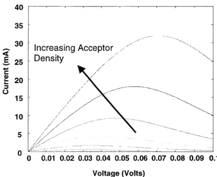
Fig. 2-8 shows the tunneling current density versus voltage for a GaAs tunnel junction doped 2x1019 cm-3 on the n-side (which results in a degeneracy of EF-Ec ~12kT at room temperature) over a range of acceptor densities on the p-side. An acceptor doping density of 6x 108 cm-3 is required to achieve degeneracy on the p-side as a result of the large density of states in the valence band of GaAs. If degeneracy is not achieved a reverse bias equal to the voltage difference between the Fermi level and the valence band edge must be applied before any tunneling commences. In the forward bias regime substantial tunneling current density and large negative differential resistance again occur only at high acceptor doping levels. If degeneracy isn't present on the p-type side of the junction then a vanishingly small number of unoccupied states are available for tunneling in forward bias with a resultant absence of forward tunneling current. Such a diode is known as a back diode. Similar but less pronounced trends result, due to the smaller conduction band density of states, from holding the p-doping constant while sweeping the donor concentration. Most importantly, with large doping values very little resistance
A-need drop across the tunnel junction to get sizeable currents. It can then be expected that the I-V characteristics of the entire BCL structure will be dominated by the voltage drops across the contacts, bulk regions and the laser diodes in the cascade. Fig. 2-9 is an enlargement of the forward I-V characteristics of Fig. 2-8. As stated above, the trend is for increased peak current at an increased voltage with increasing doping concentration. The greater degeneracy permits a greater applied voltage to reach the point where the
maximum number of occupied states on the n-side aligns with the maximum number of unoccupied states on the p-side of the junction. The increased numbers of such states
with increasing doping (degeneracy) leads to a larger peak current.
E C 0 -50 -100 -150 -200 -250 -300 -350 -400 -450_ .4 -0.35 -0.3 -0.25 -0.2 -0.15 -0.1 -0.05 Voltage (Volts) 0 0.05 0.1
Figure 2-8. Tunneling current versus applied voltage for a 20 im wide by 500 Rm long device doped 2x1019 cm-3 on the n-side. The p-type doping values are 0.6, 0.8, 1.1, 1.5, 2.1, 2.9, 3.9, 5.4, 7.3, 10xiO1 9 cm3. At high doping levels large currents flow for small applied voltages.
ensity Increasing Acceptor D
40 35 30 30 Increasing Acceptor 25 Density 20 15 10 5 .. 0 0 0.01 0.02 0.03 0.04 0.05 0.06 0.07 0.08 0.09 0.1 Voltage (Volts)
Figure 2-9. The forward tuneling currents of Fig. 2-8. The peak current increases, as does the voltage at which the peak current occurs, with increasing doping densities.
As is evident in Fig. 2-8, doping well in excess of degeneracy is required to achieve any appreciable reverse tunnel current. The substantial bandgap of GaAs (1.42 eV at room temperature) requires a sizable built-in electric field (2x10⁶ V/cm) to achieve a high tunneling probability. The exponential nature of the I-V curve in reverse bias is evident. This nonlinearity can result in signal distortion in the output of a modulated BCL. While the nonlinear nature of the reverse bias I-V characteristics cannot be completely eliminated, the deleterious effects can be minimized by reducing the resistance of the tunnel junction below that of any other in the BCL.
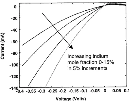
The most substantial gains in tunnel junction conductivity are realized by using InxGai xAs as the tunneling material. Fig. 2-10 shows the I-V curves of x = 0, 0.05, 0.10, 0.15 InGaAs junctions doped on both sides to 2x1019 cm-3. A 15% In mole fraction junction performs comparably to a GaAs junction doped twice as heavily. As expected, at a given doping density the incorporation of any amount of In into the tunnel junction improves the conductivity of the junction over a GaAs junction.
0 -20 -40 -60 -80 0 0J Increasing indium -100 mole fraction 0-15% in 5% increments -120 -1401 -0.4 -0.35 -0.3 -0.25 -0.2 -0.15 -0.1 -0.05 0 0.05 0.1 Voltage (Volts)
Figure 2-10. The tunneling current versus voltage for 20 gm by 500 .tm device with In mole fractions varying from 0-15% in 5% increments. The doping densities are 2x1019 cm-3 on both the n- and p-sides of the junction. Increasing the In mole fraction reduces the bandgap and effective mass leading to improved tunneling characteristics.
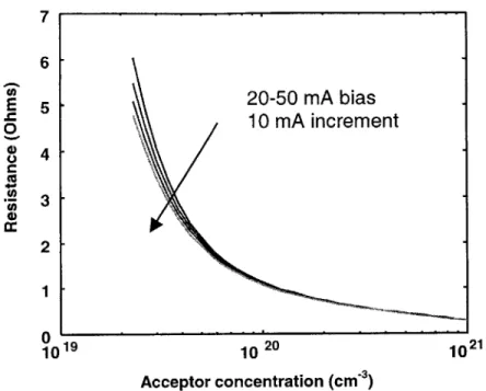
From a circuit theoretical point of view, what is of greatest interest are the large signal and differential resistances of the tunnel diodes. Fig. 2-11 shows the large signal resistance versus doping density over a range of bias points of a tunnel diode. At low doping densities, the resistance shows a rather substantial dependence upon bias point while at higher densities the junction resistance is relatively insensitive to bias. The same holds true for the differential resistance (Fig. 2-12). Holding the doping densities constant at 2x10'9 cm~3 but switching to 15% In mole fraction InGaAs from GaAs yields substantial improvement in both large signal and differential resistance (Fig.'s 12a and
12b). The advantage gained in using narrow bandgap semiconductors is diminished when very high doping densities are used. This is important in BCL structures which may contain many cascades as the accumulated strain of several In containing junctions could exceed the limit for pseudomorphic growth.
-7 6 E 0 0 5 4 3 2 1 U 1019 10 20 1021 Acceptor concentration (cm-3 )
Figure 2-11. The junction resistance versus p-type doping density of a 20 Rm by 500 pm tunnel junction doped to 2x1019 cm-3 on the n-side of the junction over a bias range of 20-50 mA. At lower doping densities the device resistance is sensitive to bias point while at densities in excess of Ix1020 cm-3 the bias point
sensitivity is negligibly small.
a:E .C C c .: 5 4.5 4 3.5 3 2.5 2 1.5 1 0.5 0 10 19 10 20 Acceptor concentration (cm-3) 1021
Figure 2-12. The differential resistance for the device of Fig. 2-11. The same trends that were evident in the resistance also appear in the differential resistance.
20-50 mA bias 10 mA increment
20-50 mA bias 10 mA increment '