HAL Id: hal-03017013
https://hal.archives-ouvertes.fr/hal-03017013
Submitted on 20 Nov 2020HAL is a multi-disciplinary open access
archive for the deposit and dissemination of sci-entific research documents, whether they are pub-lished or not. The documents may come from teaching and research institutions in France or abroad, or from public or private research centers.
L’archive ouverte pluridisciplinaire HAL, est destinée au dépôt et à la diffusion de documents scientifiques de niveau recherche, publiés ou non, émanant des établissements d’enseignement et de recherche français ou étrangers, des laboratoires publics ou privés.
High temperature operation of a monolithic
bidirectional diamond switch
Cédric Masante, Julien Pernot, Aurélien Maréchal, Nicolas Rouger
To cite this version:
Cédric Masante, Julien Pernot, Aurélien Maréchal, Nicolas Rouger. High temperature operation of a monolithic bidirectional diamond switch. Diamond and Related Materials, Elsevier, 2020, 111, pp.108185. �10.1016/j.diamond.2020.108185�. �hal-03017013�
High temperature operation of a monolithic bidirectional
diamond switch
C´edric Masante∗1, Julien Pernot1, Aur´elien Mar´echal2, and Nicolas Rouger3 1Institut N´eel, Universit´e Grenoble Alpes, CNRS, Grenoble 38031, France.
2G2Elab, Universit´e Grenoble Alpes, CNRS, Grenoble 38031, France. 3LAPLACE, INP Toulouse, CNRS, Toulouse 31071, France.
August 27, 2020
Keywords: Diamond, Electrical properties characterization, High power electronics, MOS-FET, Bidirectional
Abstract
We report the 250◦C operation of a diamond-based monolithic bidirectional switch. A normally-ON double gate deep depletion MOSFET was fabricated with a 400 nm p-type channel with a boron doping of [NA-ND]= 2.3×1017cm−3and an Al2O3gate oxide thickness
of 50 nm. The Istand IIIrdquadrants transistor characteristics are successfully measured by controlling the channel conductivity with both gates separately, with a clear ON and OFF state. A threshold voltage around 35 V is obtained with a low minimum gate leakage current of 1.00 × 10⁻⁴ mA/mm at a gate-source bias VGS = 50 V. The bidirectional switch is then
obtained by operating the MOSFET in the Ist quadrant of each gate setup. This first proof of concept offers a reverse conducting and reverse blocking diamond MOSFET, with only one drift region layer.
1
Introduction
The use of wide bandgap semiconductor material is of high interest for power electronics appli-cations, which requires devices able to withstand both large current densities and large electric
∗
fields. Diamond meets these requirements thanks to its attractive physical properties, particu-larly its high breakdown field (up to more than 10 MV/cm) and superior thermal conductivity (22 W/cm.K). A focus is made on high temperature and high blocking voltage applications in which it is considered that diamond has the greatest potential[1]. In recent years diamond based power MOSFETs have been demonstrated[2]–[7], mostly relying on the surface transfer doping effect[8] (HFET) due to their relative ease of fabrication compared to the more stan-dard MOSFET architectures (which require both p-type and n-type doping in the same device). Complementary to these structures a bulk conduction diamond MOSFET was recently intro-duced, the diamond deep depletion MOSFETs (D3MOSFET), to take full advantage of the diamond bulk properties[9]–[11]. Such diamond MOSFETs devices have been shown to exhibit a diode-like reverse conduction[12], but no reverse blocking capability, similar to SiC JFETs or GaN HEMTs[13], [14].
In several applications (e.g. matrix converters, multi-level converters, AC/AC converters), reverse conducting (RC) and reverse blocking (RB) power devices, also known as bidirectional power transistors, with the lowest on-state resistance are required. In this context, monolithic bidirectional power devices have been previously demonstrated[15]–[20], and we report here the first monolithic bidirectional diamond power FET (RC+RB) based on the D3MOSFET design. In the view of limiting the on-state resistance of the bidirectional diamond MOSFET, only one drift region is proposed with two isolated gates. Its high temperature operation and low specific on-state resistance is demonstrated in this article.
2
Device structure, fabrication and experimental method
The sample consists of a 400 nm boron-doped p-type layer grown by microwave plasma assisted CVD, on a 4 × 4 mm2 High Pressure High Temperature (HPHT) Nitrogen-doped electrically insulating diamond substrate (fig 1). This p-layer is used for the drift region of the bidirectional P-MOSFET, since boron doping is the best option for volume conduction in diamond (activation energy of boron is 0.38 eV, doping dependent, and a hole mobility up to 2000 cm2·V−1·s−1). The doping level of the p-type layer was measured to be [NA-ND]= 2.3 × 10¹⁷± 0.5 × 1017 cm−3
by capacitance voltage measurements on MOS capacitors fabricated on the same sample. This was performed at temperatures ranging from room temperature to 250◦C, with an AC signal amplitude of 30 mV and a frequency carefully chosen to avoid frequency dependent effects. This
Figure 1: a) Schematic representation of the double gate lateral p-type D3MOSFET at left, the 0.2 µm selectively grown heavily boron doped layer ([B] > 5×1020cm−3) is deposited on top of a boron doped layer ([NA-ND]= 2.3×1017 cm−3) with thickness of 0.4 µm. The metallic contacts
all consist of a Titanium/Platinum/Gold (30 nm/20 nm/30 nm) stack. b) SEM top view of one of the fabricated device.
high doping range for the drift region was chosen to demonstrate a high electric field and a high current capability with diamond FETs as previously demonstrated in[12]. To lower the contact resistances, a 200 nm of highly boron-doped ([B]> 4 × 1020cm−3) diamond is selectively grown at the source and drain contacts. A Titanium/Platinum/Gold (30 nm/20 nm/30 nm) stack is then deposited by electron beam evaporation and annealed for 30 min at 500◦C in high vacuum condition (< 10−7 mBar) to form the drain and source contacts. In order to limit the gate surface required, reducing the risk of critical failure and lowering the leakage current, a mesa structure has been designed; A reactive ion etching of O2 plasma is used to etch down
to the insulating diamond substrate around devices, as depicted in fig 1a). After an UV ozone treatment to saturate the diamond surface with oxygen bonds, the 50 nm Al2O3 gate oxide
layer was deposited following the process detailed by T. T. Pham et al. [21] to decrease the interface state density. The Savannah 100 deposition system from Cambridge NanoTech was used with a deposition temperature of 380◦C, followed by a 30 min annealing at 500◦C. Finally, the Titanium/Platinum/Gold (30 nm/20 nm/30 nm) gate metal stack is deposited by electron
beam evaporation. Elementary p-type D3MOSFETs with only one gate were also fabricated on the same diamond substrate, which showed a normally-on behavior, with a threshold voltage of +35V and a low gate leakage of 10nA/mm under a high electric field of more than 6MV/cm both in diamond and gate oxide [12] .
The measured MOSFET dimensions are LG1D = 4 µm, LG1 = LG2 = 2 µm, LG1G2 =
LG2S = 5 µm and a width of W = 60 µm. They can ideally be further reduced but were
chosen towards a first proof of concept and related to lithography and fabrication limitations. Considering the measured doping level of [NA-ND]= 2.3 × 1017 cm−3, the drift lengths should
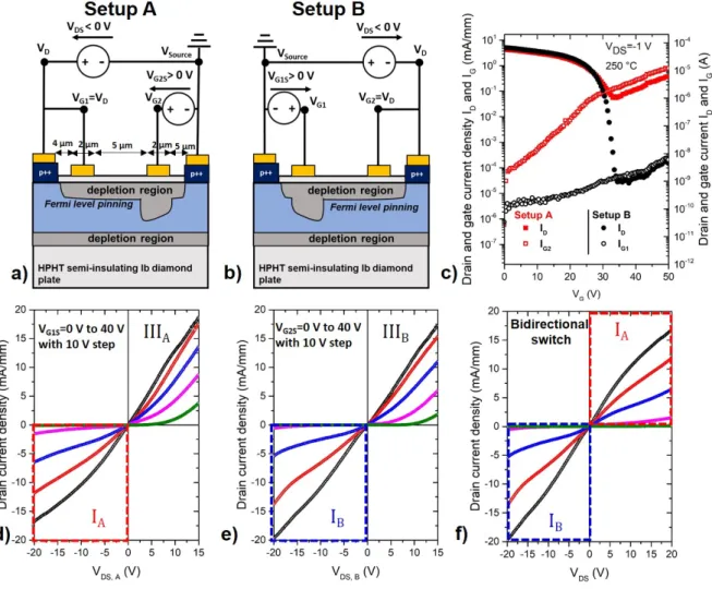
ideally not exceed 2 µm[22]. A dual channel keithley 2612 sourcemeter was used to characterize the Ist and IIIrd quadrant transistor characteristic of each setups, depicted in fig 2a) and b). To achieve a bidirectional switch, the device is always operated in the Ist quadrant of the setup A or B depending of the bias sign applied between the ohmic contacts. In setup A, the gate 2 voltage controls the channel conductivity (transistor forward bias) while the drain and gate 1 are set at the same bias. The gate to drain distance is then LG1G2+LG1+LG1D and the depleted
region below the gate 1 remains small as the drain to gate 1 potential difference is small. The setup B simply corresponds to the symmetrical case (transistor reverse bias). In this study, the switch between the two setups is performed manually to avoid the need of an external gate driver, the quasi-static bidirectional switch device characteristic is then reconstructed from both setups characteristics.
3
Results and discussion
Both setups transistor characteristics at 250◦C are shown in fig. 2d) and e). The on and off state are obtained in the Ist quadrant for a negative drain-source bias V
DS < 0 V
(p-type MOSFET). The IIIrd quadrant characteristic has been successfully measured with the two gate setup, exhibiting the distinctive reopening of the channel in a diode-like behaviour. The bidirectional switch characteristic is shown in fig. 2f), obtained with the Ist quadrant of each setups.
The minimum 250◦C on-state resistance is measured at 159 mΩ.cm2 and 152 mΩ.cm2 in setup A and B respectively, in the same order of magnitude than reported values on H-terminated MOSFETs, with a threshold of around 35 V (fig. 2c)). The on-state resistance is partially limited by the well known presence of a Fermi level pinning, at the oxygen-terminated diamond and oxide
Figure 2: Schematic representation of the double gate lateral D3MOSFET in a) the setup A and b) the setup B. When one of the gate is controlled, the other one is shorted with the closest ohmic contact. Because the experimental set-up is limited to 4 probes, the substrate is left floating. c) Measured transfer characteristics of setup A (red) and B (black), both the drain current ID and
gate leakage current IGare plotted in full and open symbols respectively. d) Measured transistor
characteristic at 250◦C in the setup A and e) the setup B. f) The Ist quadrant of both setups are then use to reconstruct the transistor characteristic of the bidirectional double gate lateral D3MOSFET.
interface[9], [21], [23], [24], accounting for an uncontrolled depleted layer at the diamond/oxide interface. This is also complemented by the probable existence of a depletion layer at the nitrogen-doped diamond substrate and the boron-doped layer. Both of these effects reduce the effective conductive channel thickness. Moreover as stated already, the device’s drift and channel length are oversized due to fabrication limitations, resulting in a larger on-state resistance.
Leakage current, shown in fig. 2c), was found to be greatly varying from one gate to the other by orders of magnitude. In the case presented here, at 250◦C gate 1 and gate 2 exhibit at a gate-source voltage VGS = 50 V a leakage current of IG1 = 0.217 mA/mm and IG2 = 1.00×10⁻⁴
mA/mm respectively. At least one of the gates in all the measured transistors exhibited a large leakage current. This prevented us from probing the off-state blocking capabilities of the device, a moderately high drain bias (|VDS| > 50 V) invariably caused the presence of a large gate
current in the same order of magnitude than the on state drain current, eventually leading to a non-reversible breaking of the oxide. The leakage mechanism has previously been reported to be traps to traps hopping in bulk oxide with interface/valence band recombination[24]. Applying a large gate bias, causing the presence of a large electric field in the oxide, may promote the bulk oxide trap formation, reducing the energy barrier between hopping sites as their average distance reduces. Controlling this trap density to a sufficiently low value even after several measurement cycles is of great importance to achieve a reliable high breakdown device. This could be achieved (i) by using a field plate architecture, reducing the well known electric field crowding effect, especially detrimental in 2D lateral devices. And (ii) by achieving a better control of the lithography and lift-off process, to reduce the roughness at the gate metal edge that is causing large local electric field crowding effects[25]. MOSFETs with a corbino geometry have been tried to avoid the presence of corners. But the lift-off process was found to be more challenging and no devices could be obtained. Given that diamond MOSFET devices are yet not optimized, the breakdown is usually not limited by intrinsic diamond properties, but rather by imperfections of the process, the oxide layer or in the diamond crystalline structure. In a single gate design with very similar sample characteristics, it has been shown that a blocking voltage of 200 V [9] and a critical field greater than 5.4 MV/cm [12] can be achieved. This is about twice larger than the critical field of SiC or GaN devices, without the use of electric field relaxation features to improve the breakdown. Optimized diamond devices could significantly improve the high power switch devices.
4
Perspectives
The fig. 3 shows the calculated 1D lateral static performances of a lateral bulk conduction diamond device with and without a recess gates design, in comparison to the measured device and reported values of bidirectional GaN HEMTs, bidirectional vertical 4H-SiC MOSFET and IGBT. A doping level dependant ideal breakdown and hole mobility with no compensation are assumed. The gate lengths and gate to source lengths are fixed at 1 µm. Thanks to its higher critical field, it is expected that diamond could reach higher breakdown voltages than GaN
HEMT devices, in the order of a few kV, with low RON, either with a bulk or surface conduction.
Lateral diamond devices could achieve similar performances than bidirectional vertical 4H-SiC devices at large blocking voltages, especially at high temperature. This is particularly valuable given the complex fabrication process of vertical bidirectional devices. Further reduction of the on state resistance could be achieved by operating in enhancement mode, either by accumulating holes at the MOS interface with a negative gate bias (p-type) or at zero gate bias thanks to the surface transfer doping effect. Similarly to what had been demonstrated with GaN and 4H-SiC, comparatively to the use of 2 devices, bidirectional switches offers a lower RON, a smaller device
area, no additional voltage drop in any operating quadrant (i.e. no diode-like voltage drop), smaller commutation loops thanks to monolithic integration and an optimal packaging with all power and driving electrodes on one side, and a thermal interface at the backside (for a lateral design).
Figure 3: Measured RON as function of breakdown voltage of the fabricated diamond MOSFET
and other reported wide band gap bidirectional devices from [15]–[17], [19]. The lines represent the calculated ideal characteristics at RT and 250◦C of the bidirectional lateral D3MOSFET device with gate lengths and gate to source lengths of 1 µm and optimized drift lengths. The dashed lines correspond to a more optimized recess gate design.
5
Conclusion
High temperature operation of a diamond-based monolithic bidirectional power switch based on a double gate diamond deep depletion MOSFET is demonstrated in this work. The low resistivity of diamond at high temperature allows to reach a current density of 20 mA/mm at VDS = −20 V, despite the design being oversized on purpose to facilitate its fabrication. The
high leakage current that may occur in one or both of the gates made impossible to measure the off state blocking voltage, but single gate breakdown measurements were previously reported with a blocking voltage up to -200 V and a critical field of at least 5.4 MV/cm. Lateral diamond bidirectional devices could be an attractive solution for high breakdown (> 1kV) and high temperature applications.
Acknowledgment
This research is partially funded by French ANR Research Agency under grant ANR-16-CE05-0023 #Diamond-HVDC and the French ministry of research. This work is supported by Labo-ratoire d’Excellence LANEF in Grenoble (ANR-10-LABX-51-01).
References
[1] N. Donato, N. Rouger, J. Pernot, G. Longobardi, and F. Udrea, “Diamond power devices: State of the art, modelling and figures of merit,” en, J. Phys. D: Appl. Phys., Oct. 2019,
issn: 0022-3727, 1361-6463. doi: 10.1088/1361-6463/ab4eab.
[2] H. Kawarada, T. Yamada, D. Xu, Y. Kitabayashi, M. Shibata, D. Matsumura, M. Kobayashi, T. Saito, T. Kudo, M. Inaba, et al., “Diamond MOSFETs using 2D hole gas with 1700V breakdown voltage,” in Power Semiconductor Devices and ICs (ISPSD), 2016 28th Inter-national Symposium On, IEEE, 2016, pp. 483–486.
[3] H. Kawarada, T. Yamada, D. Xu, H. Tsuboi, Y. Kitabayashi, D. Matsumura, M. Shibata, T. Kudo, M. Inaba, and A. Hiraiwa, “Durability-enhanced two-dimensional hole gas of C-H diamond surface for complementary power inverter applications,” en, Sci Rep, vol. 7, no. 1, p. 42 368, Mar. 2017, issn: 2045-2322. doi: 10.1038/srep42368.
[4] H. Kawarada, “High-Current Metal Oxide Semiconductor Field-Effect Transistors on H-Terminated Diamond Surfaces and Their High-Frequency Operation,” en, Jpn. J. Appl. Phys., vol. 51, p. 090 111, Sep. 2012, issn: 0021-4922, 1347-4065. doi: 10.1143/JJAP.51. 090111.
[5] H. Kawarada, H. Tsuboi, T. Naruo, T. Yamada, D. Xu, A. Daicho, T. Saito, and A. Hiraiwa, “C-H surface diamond field effect transistors for high temperature (400 C) and high voltage (500 V) operation,” en, Applied Physics Letters, vol. 105, no. 1, p. 013 510, Jul. 2014, issn: 0003-6951, 1077-3118. doi: 10.1063/1.4884828.
[6] Y. Kitabayashi, T. Kudo, H. Tsuboi, T. Yamada, D. Xu, M. Shibata, D. Matsumura, Y. Hayashi, M. Syamsul, M. Inaba, A. Hiraiwa, and H. Kawarada, “Normally-Off C–H Diamond MOSFETs With Partial C–O Channel Achieving 2-kV Breakdown Voltage,” IEEE Electron Device Letters, vol. 38, no. 3, pp. 363–366, Mar. 2017, issn: 0741-3106, 1558-0563. doi: 10.1109/LED.2017.2661340.
[7] N. Oi, M. Inaba, S. Okubo, I. Tsuyuzaki, T. Kageura, S. Onoda, A. Hiraiwa, and H. Kawarada, “Vertical-type two-dimensional hole gas diamond metal oxide semiconductor field-effect transistors,” en, Scientific Reports, vol. 8, no. 1, Dec. 2018, issn: 2045-2322.
doi: 10.1038/s41598-018-28837-5.
[8] P Strobel, M Riedel, J Ristein, and L Ley, “Surface transfer doping of diamond,” Nature, vol. 430, pp. 439–441, 2004. doi: 10.1038/nature02751.
[9] T.-T. Pham, J. Pernot, G. Perez, D. Eon, E. Gheeraert, and N. Rouger, “Deep-Depletion Mode Boron-Doped Monocrystalline Diamond Metal Oxide Semiconductor Field Effect Transistor,” IEEE Electron Device Letters, vol. 38, no. 11, pp. 1571–1574, Nov. 2017,
issn: 0741-3106, 1558-0563. doi: 10.1109/LED.2017.2755718.
[10] T. T. Pham, N. Rouger, C. Masante, G. Chicot, F. Udrea, D. Eon, E. Gheeraert, and J. Pernot, “Deep depletion concept for diamond MOSFET,” en, Appl. Phys. Lett., vol. 111, no. 17, p. 173 503, Oct. 2017, issn: 0003-6951, 1077-3118. doi: 10.1063/1.4997975.
[11] T. T. Pham, J. Pernot, C. Masante, D. Eon, E. Gheeraert, G. Chicot, F. Udrea, and N. Rouger, “200V, 4MV/cm lateral diamond MOSFET,” en, in 2017 IEEE International Electron Devices Meeting (IEDM), San Francisco, CA, USA: IEEE, Dec. 2017, pp. 25.4.1– 25.4.4, isbn: 978-1-5386-3559-9. doi: 10.1109/IEDM.2017.8268458.
[12] C. Masante, J. Pernot, J. Letellier, D. Eon, and N. Rouger, “175V, > 5.4 MV/cm, 50 mOhm.cm2 at 250C Diamond MOSFET and its reverse conduction,” en, in 2019 31st International Symposium on Power Semiconductor Devices and ICs (ISPSD), Shanghai, China: IEEE Xplore, p. 4. doi: 10.1109/ISPSD.2019.8757645.
[13] Y. Liu, S. Han, S. Yang, and K. Sheng, “Surge Current Capability of GaN E-HEMTs in Reverse Conduction Mode,” en, in 2019 31st International Symposium on Power Semicon-ductor Devices and ICs (ISPSD), Shanghai, China: IEEE, May 2019, pp. 439–442, isbn: 978-1-72810-580-2 978-1-72810-581-9. doi: 10.1109/ISPSD.2019.8757634.
[14] D. C. Sheridan, K. Chatty, V. Bondarenko, and J. B. Casady, “Reverse conduction prop-erties of vertical SiC trench JFETs,” en, in 2012 24th International Symposium on Power Semiconductor Devices and ICs, Bruges, Belgium: IEEE, Jun. 2012, pp. 385–388, isbn: 978-1-4577-1597-6 978-1-4577-1594-5 978-1-4577-1596-9. doi: 10 . 1109 / ISPSD . 2012 . 6229102.
[15] B.-R. Park, S.-W. Han, and H.-Y. Cha, “Diode Bridge Embedded AlGaN/GaN Bidirec-tional Switch,” en, IEEE Electron Device Lett., vol. 36, no. 4, pp. 324–326, Apr. 2015,
issn: 0741-3106, 1558-0563. doi: 10.1109/LED.2015.2398459.
[16] S. Mori, M. Aketa, T. Sakaguchi, Y. Nanen, H. Asahara, T. Nakamura, and T. Kimoto, “Temperature Characteristics of 3-kV 4H-SiC Reverse Blocking MOSFET for High-Performance Bidirectional Switch,” en, IEEE Trans. Electron Devices, vol. 64, no. 10, pp. 4167–4174, Oct. 2017, issn: 0018-9383, 1557-9646. doi: 10.1109/TED.2017.2732065.
[17] M. Wolf, O. Hilt, and J. Wurfl, “Gate Control Scheme of Monolithically Integrated Nor-mally OFF Bidirectional 600-V GaN HFETs,” en, IEEE Trans. Electron Devices, vol. 65, no. 9, pp. 3878–3883, Sep. 2018, issn: 0018-9383, 1557-9646. doi: 10.1109/TED.2018.
2857848.
[18] T. Ide, M. Shimizu, X.-Q. Shen, T. Morita, T. Ueda, and T. Tanaka, “Equivalent Circuit Model for a GaN Gate Injection Transistor Bidirectional Switch,” en, IEEE Trans. Electron Devices, vol. 59, no. 10, pp. 2643–2649, Oct. 2012, issn: 0018-9383, 1557-9646. doi: 10. 1109/TED.2012.2211020.
[19] S. Chowdhury, C. W. Hitchcock, Z. Stum, R. P. Dahal, I. B. Bhat, and T. P. Chow, “Operating Principles, Design Considerations, and Experimental Characteristics of
High-Voltage 4H-SiC Bidirectional IGBTs,” en, IEEE Trans. Electron Devices, vol. 64, no. 3, pp. 888–896, Mar. 2017, issn: 0018-9383, 1557-9646. doi: 10.1109/TED.2016.2631241.
[20] H. Dai, R. A. Torres, T. M. Jahns, and B. Sarlioglu, “Characterization and Implementa-tion of Hybrid Reverse-Voltage-Blocking and BidirecImplementa-tional Switches using WBG Devices in Emerging Motor Drive Applications,” en, in 2019 IEEE Applied Power Electronics Con-ference and Exposition (APEC), Anaheim, CA, USA: IEEE, Mar. 2019, pp. 297–304, isbn: 978-1-5386-8330-9. doi: 10.1109/APEC.2019.8721910.
[21] T. T. Pham, M. Guti´errez, C. Masante, N. Rouger, D. Eon, E. Gheeraert, D. Ara`ujo, and J. Pernot, “High quality Al 2 O 3 /(100) oxygen-terminated diamond interface for
MOSFETs fabrication,” en, Applied Physics Letters, vol. 112, no. 10, p. 102 103, Mar. 2018, issn: 0003-6951, 1077-3118. doi: 10.1063/1.5018403.
[22] G. Chicot, D. Eon, and N. Rouger, “Optimal drift region for diamond power devices,” en, Diamond and Related Materials, vol. 69, pp. 68–73, Oct. 2016, issn: 09259635. doi: 10.1016/j.diamond.2016.07.006.
[23] O. Loto, M. Florentin, C. Masante, N. Donato, M.-L. Hicks, A. C. Pakpour-Tabrizi, R. B. Jackman, V. Zuerbig, P. Godignon, D. Eon, J. Pernot, F. Udrea, and E. Gheeraert, “Gate Oxide Electrical Stability of p-type Diamond MOS Capacitors,” en, IEEE Transactions on Electron Devices, vol. 65, no. 8, pp. 3361–3364, Aug. 2018, issn: 0018-9383, 1557-9646.
doi: 10.1109/TED.2018.2847340.
[24] T. T. Pham, A. Mar´echal, P. Muret, D. Eon, E. Gheeraert, N. Rouger, and J. Pernot, “Comprehensive electrical analysis of metal/Al 2 O 3 /O-terminated diamond
capaci-tance,” en, Journal of Applied Physics, vol. 123, no. 16, p. 161 523, Apr. 2018, issn: 0021-8979, 1089-7550. doi: 10.1063/1.4996114.
[25] H. Umezawa, H. Gima, K. Driche, Y. Kato, T. Yoshitake, Y. Mokuno, and E. Gheeraert, “Defect and field-enhancement characterization through electron-beam-induced current analysis,” en, Appl. Phys. Lett., vol. 110, no. 18, p. 182 103, May 2017, issn: 0003-6951, 1077-3118. doi: 10.1063/1.4982590.
![Figure 1: a) Schematic representation of the double gate lateral p-type D3MOSFET at left, the 0.2 µm selectively grown heavily boron doped layer ([B] > 5×10 20 cm −3 ) is deposited on top of a boron doped layer ([N A -N D ]= 2.3×10 17 cm −3 ) with thick](https://thumb-eu.123doks.com/thumbv2/123doknet/14315492.496035/4.892.192.707.114.541/figure-schematic-representation-lateral-mosfet-selectively-heavily-deposited.webp)
![Figure 3: Measured R ON as function of breakdown voltage of the fabricated diamond MOSFET and other reported wide band gap bidirectional devices from [15]–[17], [19]](https://thumb-eu.123doks.com/thumbv2/123doknet/14315492.496035/8.892.194.712.521.911/figure-measured-function-breakdown-voltage-fabricated-reported-bidirectional.webp)
