• Aucun résultat trouvé

Visualising highly localised luminescence in GaN/AlN heterostructures in nanowires

N/A
N/A
Protected

Academic year: 2021

Partager "Visualising highly localised luminescence in GaN/AlN heterostructures in nanowires"

Copied!
19
0
0

Texte intégral

Loading

Figure

Figure 1: Acquisition scheme for spectrum imaging. On the left, in the microscope (STEM) two  kinds of detectors are used: a Dark Field Detector and a CCD camera attached at the exit of an
Figure 2: STEM-HAADF images of three different NWs from the same sample. (a) A NW with  only a well-defined QDisc system
Figure 5: Spectra extracted from the spectrum image at different positions. (a) Parts of the GaN NW either covered  with the AlN shell or not (the spectra are extracted from the regions marked with squares in Fig
Figure 6: Dependence of the CL signal intensity at λ=333 nm (a) (coming mostly from the 3 rd  QDisc) and at λ=337 nm  (b) (coming mostly from 4 th  QDisc) on the electron probe position (see horizontal lines in Figure S2(b))
+2

Références

Documents relatifs

Figure (I.1): Sites acides de type Brønsted et Lewis. 2) : Schéma de la séquence de Polarisation Croisée (CP). 3): Cycle auto-cohérent électronique pour la résolution des équations

[r]

[r]

[r]

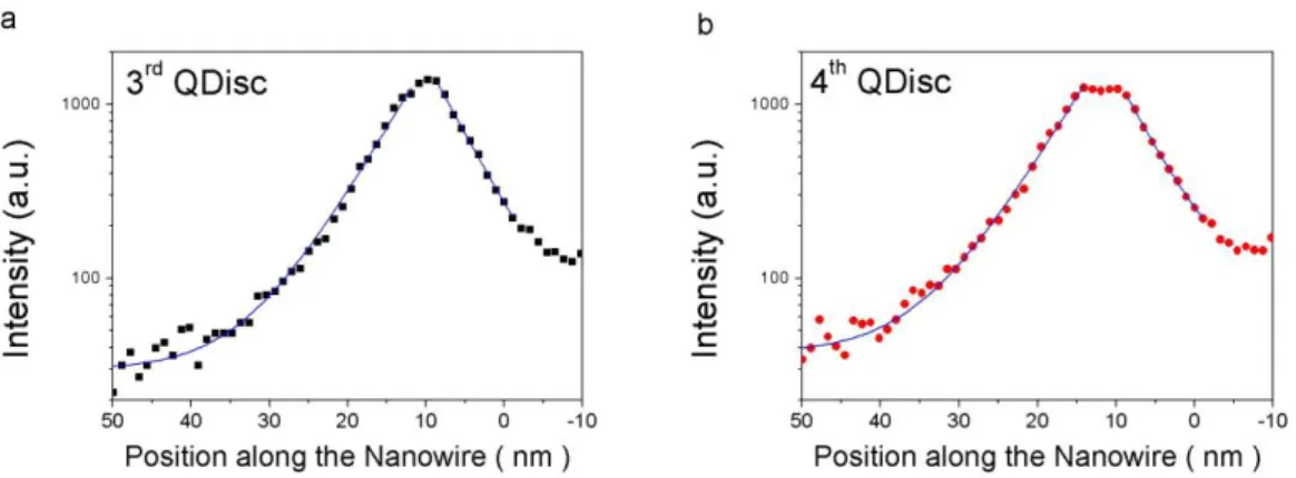
The GaN/AlN heterostructured nanowires were chosen since they represent a model system with a strong internal field and band gap engineering (similarly to InGaN

[r]

In particular, a rather noticeable behavior arises as a consequence of this level interaction: The two highest energy size dispersion curves cross at around 5 nm, so that the

We illustrate in this section the valuation of the European call option on the maximum of the instantaneous rate in the one factor affine mode bu using its explicite formula of