Design and Manufacturing of High Precision Roll-to-Roll
Multi-layer Printing Machine- Measurement and Experiment
by
by
MASSACHUSETTS INSTMIlJTEOF TECHNOLOGY
Wenzhuo Yang
DEC 2 8 2009
B.S., Industrial Engineering and Management (2008)
LIBRARIES
Shanghai Jiaotong University
Submitted to the Department of Mechanical Engineering in partial
fulfillment of the requirements for the degree of
Master of Engineering
ARCHIVES
at the
MASSACHUSETTS INSTITUTE OF TECHNOLOGY
August 2009
© Massachusetts Institute of Technology, 2009. All rights reserved.
Signature of Author:....
...epartment of Mechanical Engineering
2/
August 18, 2009
Certified by:
David E. Hardt
Professor of Mechanical Engineering
0
01
,,P
~Tesisgpervisor
A ccepted by: ...
David E. Hardt
Chairman, Departmental Committee on Graduate Studies
Department of Mechanical Engineering
Design and Manufacturing of High Precision Roll-to-Roll
Multi-layer Printing
-
Measurement and Experiment
by
Wenzhuo Yang
Submitted to the Department of Mechanical Engineering
on 14 August, 2009, in partial fulfillment of the
requirements for the Degree of Masters of Engineering in Manufacturing
Abstract
In 2008, a prototype machine demonstrating the application of roll-to-roll technology in micro-contact printing was developed. In this research, the prototype machine was upgraded by designing and machining a device that could fabricate a flat stamp with significantly less variance. The print roll wrapping system was reconfigured in order to capture the stamp with uniform force and good alignment. The motion control for the print roller and impression roller was also improved. In addition multi-layer printing with the updated machine was tested. This thesis focuses on the general design of the updated system and the measurement of key
components of the systems as well as the print quality. Results demonstrate that the flat stamp can achieve the flatness of ±16# m with thickness of 1194pm; that the wrapping process can
guarantee a a print roller roundness error in the 20pm range; that the distortion of the print using the updated system is approximately 3.8. The multi-layer printing test did not achieve acceptable results owing to a lack of proper control of the machine. However, initial trials, achieved
alignment errors of 1017 pm along the printing direction and 113pm across the printing direction.
Thesis Supervisor: Dr. David E. Hardt Title: Professor of Mechanical Engineering
ACKNOWLEDGEMENTS
First, thanks to my great teammates: Yufei Zhu, Paolo Baldesi and Charudatta Datar. We worked as a team on this project; their bright ideas and hard working help this project succeeds. Every one of them has their own specialties and strength that help me to learn not only in the project level but in many extended areas.
Many thanks to my advisor Professor Hardt, who gave us tremendous guidance and insights throughout the project. Meetings with Prof. Hardt were always enjoyable and enlightening. I am also very gratitude to our supervisors in Nano Terra: Igor Sokolik, Werner Menzi, Brian Mayers, and Shih-chi Chen. Their resources and wealth of knowledge in the science of nano-manufacturing has been invaluable and has contributed greatly to our work.
Last but not the least, I want to thank my families for their encouragement and firm support in every aspects of my life.
Table of Content
Abstract ...
3
ACKNOW LEDGEMENTS ...
... 4
Table of Content ...
2
1 Introduction ...
7
1.1 M otivation... 7 1.2 Problem Statement ... 8 13 Primary Analysis ... 9 1.4 Scope ... 10 1.5 Task D ivision ... 102 Literature Review ...
... 11
2.1 Soft Lithography... 11 2.2 Micro-contact Printing ... 1323 Existing Roll-to-Roll Equipment... 14
2.4 Stamp Casting Machine... 16
2.5 PDMS Peeling Process ... 18
2.5.1 Stress Zones at PDMS Peel-Front ... 18
2.5.2 Initiating Peeling... ... ... 19
2.6 Printing Pressure ... 19
2.7 Multi-Layer Printing ... 22
2.8 Optical Methodology System Review ... ... 24
2.8.1 Laser Triangulation Sensors ... ... ... 24
2.8.2 Interferometer Sensors ... 26
2.8.3 Fiber Optic Sensors ... ... 27
2.8.4 Con-Focal Laser Scanning Microscopy ... ... 29
3 Methodology ...
32
3.1 Stamp Casting Machine ... 32
3.2 Peeling and Wrapping the Stamp on the Print Roller ... . 34
3.2.1 Gripping the Film for Peeling ... 34
3.2.2 Methods to Generate Adhesive Force Between Backing Plate and Print Roller... 36
3.2.3 Methods to Wrap Backing Plate without Loosing Alignment ... 37
3.2.4 Analysis of Fixture System... 37
33 Precision Measurement Method ... ... 38
3.3.1 Flatness and Roundness Measurement ... 38
3.3.2 Distortion Measurement ... 41
4 Final Design: Results and Discussion ...
45
4.1 Flat Stamp Fabrication ... 45
4.1.1 Updated Flat Stamp Fabrication Device ... ... 45
4.1.2 Measurement of Flat Stamp Fabrication ... ... ... 48
4.2 Wrapping Flat Stamp onto The Print Roller... ... 55
4.2.1 Updated Wrapping System ... ... 55
4.2.2 Measurement of Wrapping Quality ... ... ... 56
43 Single Layer Printing with Updated R2R Machine ... 58
4.3.1 Introduction of the Updated R2R Machine... ... 58
4.3.2 Print Quality and Comparison with Previous R2R System... . 60
4.4 Multi-layer Printing with Updated R2R System ... 65
4.4.1 Introduction of Multi-Layer Printing Process ... ... 65
4.4.2 Measurement of Print quality ... ... 68
5
Summary and Future Work ...
72
Table of Figures
Figure 1: Illustration of the self-assembly process [2] ... 12
Figure 2: Steps Involved in Micro-Contact Printing 31... 13
Figure 3: Concept of the Machine 4] ... ... 14
Figure 4: Layout of The Three Modules in The Equipment [4] ... 15
Figure 5: The R2R M achine Built in '08 [4]... ... ... 16
Figure 6: Main Parts of Aluminum Casting Machine for Large Area Stamp, Developed by Nano-Terra LLC. ... 17
Figure 7: Illustration of separation at the PDMS-Silicon wafer boundary [22] ... 19
Figure 8: Directions of peeling force [22... 19
Figure 9: Exploded view of impression Assembly and Bill of Materials [4]... 20
Figure 10: Image of Different Load From Impression Roller [4]... 21
Figure 11: Gravure Printing Machine... 23
Figure 12: Actuation Method For Adjusting The Relative Distance Between Print Nips on The Substrate. ... ... ... ... 23
Figure 13: Simplified Sensing Method For Detecting The Relative Position Between Two Layers of Print in Gravure Printing... 24
Figure 14: Principal of Laser Triangulation Sensor [14]... 25
Figure 15: Principal of Interferometer System [51 ... ... 26
Figure 16: Total Internal Reflection inside Optical Fiber. [25] ... 28
Figure 17: Fiber Optic Probe Configuration [7... 28
Figure 18: Fiber Optic Probe Response Curve [17] ... 29
Figure 19: Principal of Con-Focal Microscopy [23] ... ... 30
Figure 20: Structure for W afer Chuck ... . ... 32
Figure 22: Sidebars Used to Align Both Chucks ... 34
Figure 23: Illustration of Pint Roller Setup Before Wrapping... ... 35
Figure 24: Illustration of the Proposed Fixture System ... 38
Figure 25: Fixtures for Flatness and Roundness Measurement ... 39
Figure 26: VERITAS VM 250 ... ... 40
Figure 27: Measurement Setting for Roundness Measurement... 41
Figure 28: The Shape of Rectangular- like Pixel... ... 42
Figure 29: The Shape of Triangular Pixel ... ... 42
Figure 30: The Array of Two Kinds of Pixels ... ... 42
Figure 31: Demonstration of the Distortion ... ... ... ... ... 43
Figure 32: Pixel Dimensions [20] ... ... 43
Figure 33: Displacement of Two Printed Layers... 44
Figure 34: 3D M odel of W afer Chuck for 12" wafer ... ... 46
Figure 35: 3D Model of Adapter of SS Chuck for 200mmx200mm Stamp Fabrication... 47
Figure 36: 3D Model of Assembly for 12" wafer... 47
Figure 37: Aluminum Vacuum Chuck Used in Last Year's Project... 48
Figure 38: Stainless Steel Vacuum Chuck Designed and Machined This Year ... 49
Figure 39: Using VERITAS 250 to measure the flatness of the vacuum chuck... 49
Figure 40: Topographic Mapping of the Previous Vacuum Chuck ... 50
Figure 41: Topographic Mapping of New Vacuum Chuck ... ... 50
Figure 42: QQplot of The Test Result of The Previous Vacuum Chuck ... 51
Figure 43: QQplot of The Test Result of The new Vacuum Chuck ... 51
Figure 44: Histogram of The New Vacuum Chuck Test Result ... 52
Figure 45: Topographic Mapping of The Stamp Fabricated Using Last Year's Device ... 53
Figure 47: QQPlot of The Test Result for The Stamp Fabricated Using New Device... 54
Figure 48: The Assemble Sequence of the SS Sheet ... 56
Figure 49: Different Print Roller used in 2008 (a) and 2009 (b) ... 57
Figure 50: Roundness Test Result of Previous Wrapping Method... . 58
Figure 51: Structure of the Flexure (Front View)1261 ... 59
Figure 52: The Updated Precision Shaft... 60
Figure 53: The updated Linear Ball Bearing ... ... 60
Figure 54: Comparison of Tapered Contact Areas Using Previous and Updated Print System ... 6 1 Figure 55: Setup for The Repeatability of the Parallelism Test... 62
Figure 56: Test Result of the Repeatability of Parallelism for Previous Impression Roller System ... .... ... ... 62
Figure 57: Test Result of the Repeatability of Parallelism for Updated Impression Roller System ... ... ... .. . ... 63
Figure 58: Distortion Along and Across the Printing Direction ... . 64
Figure 59: Diamond Pattern of Pixel Distortion in Last Year's Project ... 65
Figure 60: Position of Patterns After First Layer Printing... 66
Figure 61: Position Alignment of the First Layer... ... 66
Figure 62: Using Microscope to Align the Position of the Substrate ... 67
Figure 63: Adjustment of Second Layer printing ... 68
Figure 64: M ulti-Layer Printing Result ... 69
Figure 65: Relative Position of Two Layers... 69
1 Introduction
1.1 Motivation
Currently, nanostructures are commonly fabricated using techniques such as photolithography, electron-beam writing and X-ray lithography. Although these methods are proven technologies that provide high-quality outputs, there are inherent problems. These techniques are generally expensive, slow, and the production of large patterns is difficult. Micro-contact printing (yCP) is a promising technology in which a patterned elastomeric stamp is used to transfer patterns of self-assembled monolayer (SAMs) onto a substrate by conformal contact printing. In 2008, a group of MIT students developed a high throughput, low cost roll-to-roll (R2R) printing technique into micro-contact printing, achieving good results. They also built a prototype machine to realize the whole process in the speed of 400 feet per minute while maintaining good quality outputs.
However, the last year's machine is only limited to printing octadecanethiols, an organic ink, on gold substrates where the self-assembly characteristics (see section 2.1) of these media could tolerate big range of pressure variance applied on the substrate. Therefore, if the micro-contact printing is applied into some other media where self-assembly characteristics do not exist, a highly uniform pressure along the substrate will be critical to the quality of outputs. The pressure of previous prototype machine is provided by the contact of the print roller and the impression roller. The uniform roundness and straightness of the rollers is key to the uniform pressure along the contact area. Meanwhile the parallel contact between the impression roller and the printer roller is also very important. Therefore, if we can fabricate the print roller with the variance less than a few microns and the contact between the impression roller and the printer roller has good parallelism with high repeatability, then the roll-to-roll micro-contact printing technology could be easily applied to various printing media.
The printer roller consists of central shaft, sleeve, the backing plate and the stamp (see section 2.2). The uniform thickness of the stamp is the most critical component of the uniform roundness of the print roller. Currently, there is no standard process to fabricate the stamp with the thickness variance of a few microns, therefore, the repeatable, reliable and manufacturable stamp fabrication process is also highly desired.
Another limitation of last year's project is that the registration of multiple layers on a flying substrate was not considered; only monolayer could be printed using the prototype machine. However, in the industry, multi-layer printing is required, which means to print another layer on the substrate with patterns. At present, the commercial printing industry, where multi-layer printing is very common and popular, can only achieve a resolution of 40 microns. Thus, such technology can hardly be applied to multi-layer printing where the pixel size is less than 40
microns. If multi-layer printing with the resolution of 1 micron could be demonstrated by upgrading the previous prototype machine, there will be a significant impact in the printing industry.
Research was funded by and in cooperation with Nano Terra Inc, a Cambridge, Massachusetts company that specializes in Soft Lithography.
1.2 Problem Statement
The primary objective of this project is to address the limitations of the previous prototype machine in related to the potential manufacturing of printed electronics using micro-contact printing technique within the soft lithography (SL) field.
At first glance, the main goals of this project can be split in two major areas:
Improve the printing quality, upgrading the R2R system built by the MIT students in 2008; in particular this goal will be achieved by designing and fabricating an interchangeable stamp on the roller that allows a quick replacement of the stamp once it is used up, without losing of
alignment. This goal is achieved by performing four key steps:
o Design of an interchangeable stamp
o Fabrication and demonstration of interchangeable stamp o Test results providing data on distortion, alignment o Budget estimate for manufacturing applications
The second main goal of the project is to improve the overall R2R system. This task is achieved by executing the following steps:
o Redesigning and implementing the impression roller system o Designing process for multi-layer printing
o Designing high precision positioning system for the print roller adjustment o Test results providing data on distortion and alignment
13 Primary Analysis
We considered the two major goals of the project, namely, fabricating a very flat stamp and then wrapping it around the print roller, and proving that micro-contact printing can be used for printing multiple layers with alignment.
In order to fulfill these goals, our approach consisted of accomplishing the followings:
1. Flat stamp fabrication. To achieve this, a new method was developed to fabricate the stamp using a molding process, to ensure a flat and defect-free stamp.
2. Wrapping the stamp with backing plate onto the roller with alignment and repeatability. The goals of this process were to wrap the stamp while maintaining alignment, and developing a repeatable process; and to maintain uniform roundness of the stamp after wrapping. To achieve this, after looking at a lot of options, we decided to use a magnetic cylinder, and a pin-slot system to grab the edge of the backing plate. We also considered a fixture system to wrap the stamp with backing plate on the cylinder.
3. Ensuring the roundness of assembled print roller within 4 microns tolerance. With proper wrapping method, minimal and uniform printing pressure could be achieved and hence realized good printing quality.
4. Redesigning the impression roller system to improve its repeatability of parallelism. In this process, we built up error budget model, found out the constraint to the repeatability of the impression roller system and then updated the system.
5. Designing a high precision position system to control the print roller position and orientation. This step was fundamental to improve the quality of single layer printing as well as the multiple layers printing.
6. Printing using the updated machine and comparing results that achieved by last year's group. After we qualified the wrapped stamp and impression roller system, we mounted the new roller onto the current machine, to get a direct comparison of print quality. 7. Printing multiple layers as a proof of concept. This was an independent step, to prove that
micro-contact printing can print multiple layers on a single substrate with minimum misalignment.
1.4 Scope
Our project only dealt with micro-contact printing with PDMS as the stamp and 300mm wafer as the master. We focused on printing thiol onto gold-coated substrates. This scope allowed us to decide the dimensions of our design based on available materials. The mature printing mechanism also allowed us to verify our designes without disturbance of different printing conditions. For multi-layer printing, the initial purpose was to use rigid and transparent material (glass) as the substrate to print two layers using the same stamp to print twice. Later on, the scope switched to using updated R2R machine to print two layers with the same stamp in order to demonstrate what is the best alignment can be achieved using current Roll-to-Roll technology. In order to achieve this target, precise control of the printer roller on its alignment is required and we assumed the motion of the flexible substrate is self-aligned across the printing direction.
1.5 Task Division
This thesis is based on a team project executed as part of the Mechanical Engineering Master of
Engineering in Manufacturing Degree Program. The team members were:
Wenzhuo Yang has researched and determined the measurement methods for cylinder roundness, tolerance of stamp fabrication parts as well as the print quality of output features. He designed the measurement structure and analyzed the data obtain from both measurements. In addition, he worked with Yufei Zhu on the upgrade of impression roller system and multi-layer printing process design.
Paolo Baldesi has designed the high precision positioning system to control the position of the print roller. He calibrated the system and determined its performance. In addition, he worked with Charudatta Datar in developing an innovative wrapping process designing a new magnetic print roller. He also researched and designed the mechanism of growing UV-curable material onto cylinder directly.
Charudatta Datar has designed the magnetic roller, and developed the technique to attach and wrap the backing plate and PDMS stamp onto the print roller. He also worked with Paolo Baldesi in designing the high precision positioning system. In addition, he designed other components, compatible the high precision positioning system, to mount the new print roller on the machine built by the MIT '08 team.
Yufei Zhu designed prototype machine for the multi-layer printing for rigid substrates. He also designed the stamp fabrication parts with Mr. Werner Mezi from Nano-terra Inc.
We collectively tested the machine and determined the quality of printing resulted from the machines. Since we were working on a common project, the first three Chapters of our individual theses are common.
2 Literature Review
This section summarizes the existing R2R machine developed in 2008 by Adam Stagnaro, Kanika Khanna, and Xiao Shen [4,2021, introduced the technologies used in the machine, and described its
structure, function, operation steps and the result achieved. Also some pioneering studies of the currently multi-layer printing technology were reviewed to enlighten our prototype design on current R2R machine. Finally, some popular and representative optical metrology systems are studied to search out proper methods for measuring the quality of the machine design and the print output.
2.1
Soft Lithography
Photolithography is a well-established micro-fabrication technology, being widely used to manufacture most integrated circuits. It is, however, limited to a feature size of about 100 nm owing to optical limitations. Technologies such as extreme UV lithography, soft X-ray lithography, electron-beam writing, focused ion beam writing, and proximal-probe lithographylu are capable of manufacturing smaller features, however, they are limited by high cost and technology development.
Photolithography also has other limitations: it cannot be used on non-planar surfaces; it is incapable of producing three-dimensional structures, and it is not suitable for generating patterns on glass, plastics, ceramics, or carbon [1]
Thus, a family of techniques called as soft lithography, including, microcontact printing, replica molding (REM), microtransfer molding (mTM), micromolding in capillaries (MIMIC), and solvent-assisted micromolding (SAMIM) are emerging as prospective solutions to overcome some of the limitations of photolithography.
They offer a number of basic advantages, such as, little capital investment, and simplicity. Apart from these, soft lithography techniques can produce features smaller than 100 nm, with relatively simple technology, and they are not subject to optical limitations. They also offer flexibility in terms of surface material, and shape, overcoming some of photolithographic limitations.
These techniques are referred to as "soft lithography" because each technique makes use of flexible organic materials as opposed to rigid materials to achieve pattern transfer to the substrate. Basically, these techniques involve the fabrication of an elastomeric stamp (typically made of Polydymethylsiloxane, PDMS), generating a replica of the pattern originally on a Silicon master, and using this stamp to print the pattern on a substrate using self-assembly.
Self-assembly refers to the spontaneous formation of molecules into organized structures by non-covalent forces. The resulting structure is highly uniform, defect-free owing to thermal
equilibrium, and in the lowest energy form.
Self-assembled monolayer (SAM) is one such non-biological self-assembly system (see figure 1 for its process). SAMs is used in soft lithography to transfer the pattern on the elastomeric stamp, onto the surface of the substrate using minimal contact pressure.
Selfm
gurmbk
As
-ea
inroses, moeculesKsermbie to form the o*wst L
eeergy econiguraron
Ai
Figure 1: Illustration of the self-assembly process [2]
We lay emphasis upon one of soft lithography techniques, micro-contact printing, because we used this method throughout the project. This paper does not describe the other methods.
2.2
Micro-contact Printing
The micro-contact printing process involves transferring a pattern on an elastomeric stamp onto the surface of a substrate by the formation of a monolayer of ink, which can be used as resist in subsequent etching, or other steps. This process relies on SAM, in which it enables transfer of only a monolayer of ink to the substrate. This molecular level contact makes the process independent of excessive ink being trapped between stamp and substrate, allowing significantly smaller sized (~ 50 nm) features to be printed onto the substrate.
o h ,,h{Po -mrn
Figure 2: Steps Involved in Micro-Contact Printing [3]
The micro-contact printing process, as shown in figure 2, involves, like all soft lithography techniques:
1. A master with the original pattern on it. This is typically a patterned Silicon wafer. 2. This pattern is then replicated on a PDMS stamp by casting or molding.
3. This PDMS stamp is then inked, by a couple of methods (using an ink pad, or pouring ink over the stamp).
4. Next, this inked stamp comes into contact with the substrate that is to be printed upon.
5. This contact enables the formation of a SAM of the ink on the surface of the substrate. 6. The stamp is released, and the SAM formed on the substrate is then used in subsequent
etching steps to generate the required pattern on the substrate.
23
Existing Roll-to-Roll Equipment
The MIT'08 team's (Adam Stagnaro, Kanika Khanna, and Xiao Shen [420,21]) task was to take this demonstration to the next level, and prove that the paradigm would be competitive with commercial printing systems in at least one of the parameters -quality, rate, flexibility.
The key goal of this MIT'08 project was to achieve Micro-contact printing at very high speeds (400 ft/min), on 8" wide coated substrate (web).
DRIVE ROLLER
TENSION SENSOR IMPRESSION CYLINDER
IVWth load cel to monitor print pressure
STAMP CYLINDER
(Driven) A INING CYLINDER / (removable)
Figure 3: Concept of the Machine [4]
The concept of the machine is shown in figure 3. The substrate was in the form of a web, driven through a set of rolls. A combination of open and closed loop using motors and clutches was used to achieve tension control.
The equipment can be divided into three modules: Supply Module (to unwind substrate web),
Print Module (to ink, print, and apply pressure), and Collect Module (to rewind substrate web) [4]
Figure 4 shows the layout of the machine, in terms of these three modules. The entire roller system is cantilevered about a common base plate. And figure 5 shows the physical appearance of the R2R machine built by 08' group.
Print Modue C~ec Mlhodul
Suppl Module
Figure 4: Layout of The Three Modules in The Equipment [4]
We shall not describe the operation of the machine in much detail, but will emphasize on the results of the print module only, as this was felt to have the most significant impact on the results, which also have been described in detail later in this document.
Figure 5: The R2R Machine Built in '08 [4
A series of experiments were designed and conducted to test the printing quality. Below is a summary of relevant results [4]
1. Neither printing pressure nor speed was found to have a significant effect on spatial distortions and pattern dimensions in the range of settings we used.
2. It is possible to print a robust etch-resisting SAM at very high speeds (400 ft/min, unit area contact time ~ 5ms).
3. At very high speeds (400ft/min), some systematic air trapping was observed
4. The alignment of the stamp on the backing may have a significant effect on distortion patterns.
These results have formed the basis for our project. Improvements in the following were seen as critical to improving the printing quality:
1. Alignment of the stamp on the backing, and therefore on the print roller 2. Fabrication of a flat stamp
3. Precision in the web handling system of the equipment
2.4 Stamp Casting Machine
Stamp fabrication is essential to improve the quality of printing. Micro-contact printing requires precise transfer of patterns with minimum distortion and maximum yield. In addition, the stamp needs to maintain an exactly complementary pattern to the master, and it should avoid distortion during printing.
PDMS as the material for stamp has a low Young's modulus; therefore, under tension or external force, the PDMS will distort and result in a distorted pattern. In previous projects, PDMS has been cast onto a rigid backing plate. The backing plate is treated with a plasma and surface treat chemicals to increase its adhesion to PDMS, andthe force between this backing plate and PDMS is firm enough that little relative motion between the stamp and backing plate will happen. Thus, the backing plate with PDMS minimizes distortion when wrapping the stamp onto the print roller. With the consideration of cost and efficiency, large stamps are desired for production. In common practice, round wafers (150mm, 200mm and 300mm size) are used as the master and etched out negative pattern on the SU-8 layer on the master. This photo-resist will directly contact PDMS during the practice, thus caution should be made in order not to destroy the pattern on the master. The size of the stamp is limited by the size of wafer. In this project we targeted 300mm wafer as our master and explored the problems including distortion, uniformity, peeling force from master and repeatability with the capability of scaling in manufacturing.
In previous research at Nano-Terra LLC, the thickness of the stamp was shown to affects the pattern transfer and a thin stamp seems to result in better printing quality. This research is not restricted to self-assembly monolayer printing, For applications in which pressure is critical to the quality and yield of printing, the elasticity property of the stamp will be key consideration and this property is directly affected by the thickness of stamp. A uniform, thin layer of stamp is beneficial to other on-going projects in the soft lithography.
Nano-Terra developed their first casting machine (see Figure 6) using aluminum with a 12" master, which demonstrated capability of large area stamp fabrication. In figure 6, a vacuum chuck at the left hold the backing plate and flips onto the wafer chuck at the right where the wafer sits. PDMS is injected into the gap between backing plate and wafer.
Vacuum Chuck Wafer Chuck with 12" Wafer
Figure 6: Main Parts of Aluminum Casting Machine for Large Area Stamp, Developed by Nano-Terra LLC.
As shown in figure 6, this configuration is to have two vacuum chucks : one attaching the master and the other attaching the backing plate. A dam (or reservoir) is placed around the area. These two chucks face each other, and create a space, which is circled by the dam. Liquid PDMS is injected into the area with a syringe.
This pilot stamp fabrication equipment demonstrated consistent quality for use in large size stamp. However it is not designed for interchangeable masters because its mechanism for fixing the master does not allow quick uninstall. Also the space between backing and can't be adjusted easily. Thus it was not able to experiment for manufacturing purpose. Surface finish of the vacuum chuck is rough, which results in uniformed thickness across the stamp.
To resolve these problems identified from this pilot PDMS casting machine, a better material that is capable of ultra-high precision machining is necessary. The Wafer chuck will be modified to add-in alignment capability for maintaining repeatability each time a new master is brought in. Thickness of stamp can be varied by changing the spacing part between wafer and backing plate. This is the topic of Yufei Zhu's thesis [24], detail explanation on stamp fabrication process could be found in his thesis.
2.5 PDMS Peeling Process
The peeling process is a crucial step where we need to wrap a PDM stamp, which initially lies flat on a Silicon wafer, onto the print roller. Thus, it is essential to first successfully peel the PDMS stamp without any tears or distortions. This section studies some of the research that has been done on peeling PDMS off Silicon wafer.
2.5.1 Stress Zones at PDMS Peel-Front
Considerable research has been done on peeling PDMS off a Silicon wafer. However, the upper side of PDMS is not attached to any other surface (like a metal plate), but is open to air. In our project, the topside of PDMS is attached to a steel backing plate. However, some of the findings of the research are indeed useful despite this difference, and are as below.
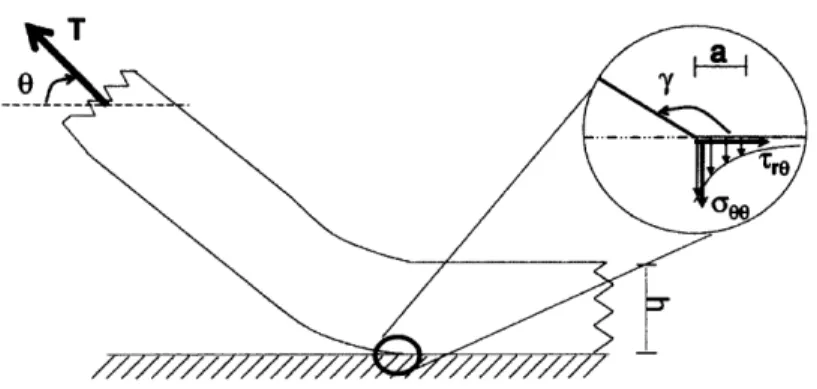
In general, at the peel front, boundary conditions are different on the two sides of the PDMS stamp; in fact, on one side, the surface of the film has zero shear stress (or very small shear stress, in our case) because it is not attached any surface (or to a different surface), while on the other side, the film adheres to the silicon master and shear stress is imposed on it by the substrate. This configuration creates a singularity around the peel front. This very small and thin zone is
characterized by a highly variable stress values. This stress singularity in the normal direction causes the separation of the film at the peel-front.
When viewed closely to the peel front, peeling of PDMS could be schematized as below:
Figure 7: Illustration of separation at the PDMS-Silicon wafer boundary [221
2.5.2 Initiating Peeling
Generally, to initiate the peeling operation we need apply a force at the peeling front, and as shown in figure 8, this force can be applied either, A: an upward force on the top surface of the film or B: a force applied at the edge on the bottom surface.
Previous works showed that, the success of either approach depends on how close the applied force is to the vertical plane of the peel-front. Only when the force is applied in the same vertical plane as the edge, the singularity at the edge results in peel-initiation.
P
Film Film
Substrate Substrate
Figure 8: Directions of peeling force [22]
2.6
Printing Pressure
Since the scope of Nano-Terra 2008 group was limited to monolayer printing using SAM as the conformal printing surface, pressure has low effect on the printing quality. The experiments carried out in 2008 indicate that when printing pressure falls in the range of 15.88kPa to
41.14kPa, or within overall load of 3.51bs to 26.81bs, quality of printing is not affected by change of pressure [4]. Because of this character of SAM, the design did not require high precision on the
printing area.
Since the machine is designed with three main modules, each module has minimal interaction, thus allowing module upgrade for different purposes. As mentioned before it was built to test the highest achievable throughput using the micron-contact printing technology.
Figure 9: Exploded view of impression Assembly and Bill of Materials [4]
We focused on improving the impression module at the center of this machine (see figure 9 for the explosive view of impression roller system). The Impression Roller Assembly will be replaced (Item #5). The goal of this improvement is to increase the repeatability of web position as well as web path. We also brought pressure sensor into the machine, enabling pressure adjustment for this machine. All these new improvements are beneficial for future applications other than self-assembly printing. These applications require better pressure control as well as
ITEM DESCRIPTION
QTY.
1 IDLER ROLLER ASSY 1
2 8020 STANDOFF 2
3 IMPRESSION FIXED PLATE 1
4 SHAFT MOUNT 2
5 SHAFT SUPPORT PLATE 1
6 LINEAR BALL BEARING 2
7 LOAD CEIL 2
8 PRESSURE PLATE 1
9 LINEAR SHAFT. .750" 2
repeatability during printing. We also expected to make the machine more accurate in web handling and the print roller adjustment, both of which are the foundation for multi-layer printing. In previous project the pressure as printing parameter has been tested. The experiments were carried out by loading impression roller onto a stationary inked printing roller with a strip of substrate in between. Thus the developed patterns after represent the actual contact area between impression roller and printing roller. Because the alignment is not easy to achieve in the print roller, the impression roller and print roller are not parallel and the contact area is tapered, as shown in figure 10.
iPRUnIU LOI
Figure 10: Image of Different Load From Impression Roller [4]
To investigate the reasons for non-parallel contact, an error budge was carefully studied. As show in table 1, the built-up error of all these components is small compared to error introduced by weight. Under 3.5 pound pressure, the right stripe in figure 12 has top width as 0.09 inch, and bottom width as 0.23 inch4 ][
Table 1 List of Parts in Impression Assembly
Item Description Qty IManufacturer endor Part # Error
1 MODULE PLATE, PRINT 1 NT-MIT MD Belanger P101 0. 075mm/40cm
2 SHAFT SUPPORT PLATE 1 NT-MIT MD Belanger P114 0. 075mm/40cm
3 IMPRESSION FIXED PLATE 1 NT-MIT MD Belanger P116 0. 075mm/40cm
4 IDLER ROLLER ASSY 1 DFE DFE IR3-8-45 N/A
5 LINEAR BEARING ASSY 2 THOMSON M-C 64825K36 N/A
6 LINEAR SHAFT, .750" 2 THOMSON M-C 6649K61 0. 002"/12"
7 SHAFT MOUNT 2 M-C 6068K27 N/A
8 8020 STAND OFF 2 8020 N/A
2.7
Multi-Layer Printing
After the successful demonstration of high throughput and good yield in one-layer printing using R2R machine, our background knowledge is sufficient to start the research in micro-contact printing's capability of multi-layer printing. This is an important step towards the actual
application in manufacturing because micro-contact printing is no longer limited to printing of photo-resistive material as the ink. Further applications require multiple layers to overlap to
achieve complex function. The units under consideration include diodes and transistors with at least 3 layers.
An important specification introduced in multi-layer printing is accuracy in relative layer position or registration. We are expecting to achieve registration with the roll-to-roll structure, because of the high throughput. However most literature discusses methods to align surface to surface, including the alignment between mask and wafer in semiconductor industry, or dip and substrate in inkjet printing, while few have mentioned alignment issue between round subject and flat substrate. Thus references for designing machine capable of multi-layer printing will be mainly from color printing industry.
It is common practice to start building high precision system based on an open-loop structure and to add-in close loop component to increase the accuracy. An open-loop structure is simple because micro-contact printing requires only two motions: linear motion of substrate and rotational motion of the print roller. Since roll-to-roll machines are widely used in printing
industry, it is beneficial to learn how the feedback systems work. We will use gravure printing to demonstrate how the printing industry achieves this registration. Figure 11 shows a typical gravure-printing machine.
S ... -,
Figure 11: Gravure Printing Machine.
Gravure is widely used in high quality printing. Because human eyes are not sensitive to features less than 40 micron wide, the feedback system for gravure machines usually set the accuracy at
100 micron or less. Errors in two key directions have been compensated. One is the direction of substrate motion during printing, or the "path"; the other is the direction perpendicular to the path on substrate plate. The latter is easy to adjust by moving roller along its axis; the error in path is sensed and compensated using sleeve displacement between the roller and the sleeve (see figure
12).
Red
Figure 12: Actuation Method For Adjusting The Relative Distance Between Print Nips on The Substrate.
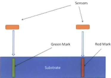
In Gravure printing, marks are printed with a distance of 20mm, and individual roller prints each color mark. Sensors are used to check the distance between marks to determine the relative position between different colors on substrate. The sensor system is shown in figure 13. The signal from sensors are received only when designated color are about to arrive. Once an error is detected, the controller will send out signals to the roller whose color is offset from its desired position, and the sleeve on the roller will rotate to compensate for this error.
_ I_~~~_
_--- --
|-PI
Green Mhar. Red Mir
Figure 13: Simplified Sensing Method For Detecting The Relative Position Between Two Layers of Print in Gravure Printing.
Assume both red and green rollers are rolling at the same speed, the green and red mark on the substrate will have a constant distance of 20mm, and signals from both sensors will reach controller at the same time. If, however the green roller is one step behind compared to the red roller, the green mark will shift back at some distance, and a signal from the green sensor will lag from the red signal. The controller will determine the amount of offset from the time of this lag and control the sleeve on green roller to shift one step ahead.
2.8
Optical Methodology System Review
One of the objectives of the project is to fabricate the stamp within the variance of ±4y, which means high precision measurement tools has to be employed. Currently, there are various kinds measurement sensors that can achieve very high accuracy and resolution, but they also have specifications that match some specific needs. In this section, laser triangulation sensors,
interferometers, fiber optic sensors and con-focal microscopy are reviewed as our potential choice of measurement sensors.
2.8.1 Laser Triangulation Sensors
Triangulation measurement is an old but very useful method to measure distance. Laser sensor is a powerful tool, using triangulation measurement, to measure either long-distance or
very high resolution. Laser sensor projects a spot of light onto the target and receives the reflected light with photo detector through an optical lens. A typical laser triangulation system is shown in Figure 14 below. Laser diode
cCD
o
-
-C
suraCes--Figure 14: Principal of Laser Triangulation Sensor [14]
From the figure 14, we could see that the relative position of laser diode, lens, photo detector and the position of reflected light from the target on the photo detector determine the distance of the target. If the target changes it position, the reflected the light changes its position on photo detector as well. Through linearization and additional digital or analogue signal processing, the detector could provide an output signal proportional to the position of the target. The ambient light has little effect on reading, because the signal is proportional to the center of intensity of focused image [14]
The most important part of laser sensor is the photo detector, which could be photo diode, position sensitive device (PSD), charge coupled device (CCD), Complementary
metal-oxide-semiconductor (CMOS), etc[14]
. Different photo detector requires different signal processing method.
The following summary of general laser triangulation sensors' characteristics is built upon the works done by Alexander H. Slocum in his book named Precision Machine Design "16, updated with recent industry standards. Note that the manufacturers are always advancing the state-of-art, so this summary is generalization only.
Size: Typically 30x50x70mm
Measurement Range (span): 3 -1300mm
Accuracy (linearity): 0.03% of Span, 500 Hz, to white target (85% diffuse reflectance) Repeatability: Depends on the repeatability of the surface finish.
Resolution: on the order of 0.005% of full-scale range, could achieve as high as 0.1P Laser spot size: 30-300pm
Environment Effect on Accuracy: On the order of 0.01%/oC of full-scale range from the nominal 200C operating temperature
Power: 15 - 24 Volts DC, 120 - 200 mA draw with 350 mA surge at power-up
Allowable Operating Environment: Keep optical windows clean for best performance. System
typically operate from 0 to 40 OC
2.8.2 Interferometer Sensors
Various kinds of interferometers are in use today. Michelson interferometer has the most common configuration for optical Interferometry and was invented by Albert Abraham Michelson. A typical and simplified interferometer system is shown schematically in Figure 15.
mirror half-silvered coherent miror light source mirror detecaor
Figure 15: Principal of Interferometer System [15]
According to figure 18, a continuous light source was spitted into two paths: One bounces back from the semi-transparent mirror, and then reflects back from the mirror on the top, goes through
the semi-transparent mirror, to the detector. The other one goes through the semi-transparent mirror, bounces back from the mirror at right, and then reflects back by the same semi-transparent mirror and goes into the detector. Difference in path may result from the length difference or different materials, which cause alternating pattern on the detector. If no difference of materials involved in the interference, the distance could be measured through
The following summary of general laser triangulation sensors' characteristics is built upon the works done by Alexander H. Slocum in his book named Precision Machine Design [16], updated with recent industry standards. Note that the manufacturers are always advancing the state-of-art, so this summary is generalization only. It is also extremely important to stress that the accuracy of measurement is highly depended to the manner of how the optics are mounted and how the environment are controlled.
Size: Laser head, 130x 180x530mm.
Cost: About $9000 for laser head and electronics boxes for up to 4 axes of measurement. Measurement Range (span): up to 30m[161
Accuracy: In a vacuum, if perfectly aligned, the accuracy can be on the order of half (worse) the
resolution. As for non-vacuum conditions, the environment significantly impacts the accuracy of measurement.
Repeatability: Depends on the stability of the environment and the laser head.
Resolution: Depends on optic used and can be achieved as high as k/4096. Higher resolution
could be achieved through better optics and phase measurement technique involved.
Environment Effect on Accuracy: About lpm/m/C Air turbulence and thermal expansion of optics, mounts and the machine itself [16]
Power: 12 V, 200 mA (PICO M8 con.)
Allowable Operating Environment: Since the interferometer is sensitive to the environment,
ideally, it should be used in a vacuum, or in air of 200C with no gradients.
2.83 Fiber Optic Sensors
Optical fibers are glass or plastic fibers that transmit light using the property of total internal reflection and the fiber act as waveguide [25]. Figure 16 demonstrates the total internal reflection of a laser inside the optical fiber.
Figure 16: Total Internal Reflection inside Optical Fiber. [25]
The key elements for fiber optic sensor are two sets of flexible probes: one is for transmitting and the other is for receiving. Two probes are jacketed into one to measure the distance. There are basically three kinds of probes configurations: Hemisphere, Random and concentric, as shown in Figure 17. Active diameter of probes could be as small as 0.177mm, making them ideal to measure small target [17]
Random CONCENTRIC (R) TRANSMIT INSIDE (CTI * RseelvhgFir o Tmraitng Fler Hemispherical (H)
Figure 17: Fiber Optic Probe Configuration [17]
The distance of an object can be determined based on the intensity of reflected light that is sensed by two transmitting and receiving fiber probes [181. The response curve is shown in Figure 18, and the intensity of reflected light is converted to voltage output. Optic Fibers are not sensitive to electromagnetic interference and typically very light [16]
DISTANCE FROM PROBE TO SURFACE
(DISPLACEMENT
Figure 18: Fiber Optic Probe Response Curve [17]
The following summary of general laser triangulation sensors' characteristics is built upon the works done by Alexander H. Slocum in his book named Precision Machine Design [16, updated with recent industry standards. Note that the manufacturers are always advancing the state-of-art, so this summary is generalization only.
Size: cable diameter could be Imm or even smaller
Cost: Depends on the type of sensor, $100-$1000.
Measurement Range (span): a few millimeters for small displacement (<10mm) Accuracy: 0.1% of full range;
Repeatability: Depends on environment conditions
Resolution: Can achieve very high resolution if the sensor held very close to the target, like
0.0 1pm resolution with the range of 0.1mm
Environment Effect on Accuracy: very sensitive to environment, like dirt on the sensor will degrade the performance.
Allowable Operating Environment: Since the interferometer is sensitive to the environment, the
sensing surface must be kept very clean. Individual probes should be kept away from moisture, or they will eventually erode to the point of failure.
2.8.4 Con-Focal Laser Scanning Microscopy
Con-focal laser scanning microscopy (CLSM or LSCM) is a technique that could capture very sharp optical images at selected height [23]. A very important feature of con-focal microscopy is
that it could obtain images from various depths. Because of its high resolution on depth
measurement, the con-focal microscopy could be applied to measure the flatness of object within the limitation of the measurement tool.
In con-focal laser scanning microscopy, a coherent light source projects a beam of laser, which goes through the beam splitter and focused on the target via lens. Scattered and reflected laser light, together with the illumination light, were re-collected by the lens and then focus on the detector via the reflection of the same beam splitter. The aperture of detector blocks the light that is not from the focal point and hence leads to a sharper image comparing to conventional
microscopy. (See figure 19)
Beam splitte Light sourc n. - Aperture -Light detector u0
U-Figure 19: Principal of Con-Focal Microscopy [23]
Adjusting the position of lens could allow light detector capture the sharpest image of the targeted area. Most of current con-focal measurement systems are using CCD to detect the target and measure its position.
In this project we are using Nikon VERITAS VM250 as our main metrology to test the surface flatness through measuring the depth of the sample points. The following is the summary of general characteristics of Nikon VERITAS product series.
Size: Main body -565 x 690 x 740 mm (minimum height), 72kg; Controller - 145 x 400 x 390 mm, 13kg
Cost: Depends on the type the precision and measurement range, more than $10,000 Measurement Range (span): could achieve 50mm
Accuracy: could achieve 1 ym
Repeatability: rely on xyz moving stages
Resolution: Can achieve 0.1 m
Power: AC 100-240V±10%, 50/60Hz
Environment Effect on Accuracy: within allowable operating environment, the accuracy can be well maintained
3
Methodology
3.1 Stamp Casting Machine
Before processing the casting machine compatible with 12" master, we started with a 6" casting machine to see the capability of the design and building material (316 Stainless Steel). The design allows both 150mm wafer and 200mm wafer to be used in the same configuration. The
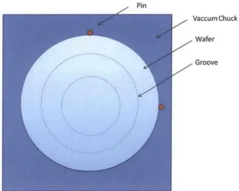
stamp-casting machine will be capable of alignment for different masters. We use pins to locate wafer. In order to hold tight the wafer during pouring PDMS, grooves are designed for vacuum capability and wafer will be held using vacuum after aligning (see figure 20). Because no glue or tape will be used in the process, wafer will be easily replaced once the vacuum has been turned
off.
Pin
Vaccum Chuck Wafer
Groove
Figure 20: Structure for Wafer Chuck
A single piece of Teflon with a rectangular opening inside will attach to master as the dam for holding PDMS within the area, this Teflon will also act as spacer between master and backing plate (see figure 21). Shape and the thickness of the stamp on the backing plate are determined by this Teflon.
Outline of master
Figure 21: Teflon Spacer
The area for containing PDMS is confined by:
1. Wafer on the top for transferring pattern;
2. Thin stainless steel sheet (backing plate) sitting at the bottom as the backing for PDMS; 3. Dam between wafer and backing plate for holding the PDMS.
Repeatability is the critical design specification. Under this configuration, making a single big stamp will require many identical steps, and each step will result in a small area of finished stamp. Variables to be considered are:
1. Distance between master and backing plate (all attached to the chuck)
2. Displacement between master and backing plate 3. Uniformity of the stamp
All these variables can be decomposed in 6 dimensions: 3 linear and 3 rotational.
A sidebar is used to align both chucks, as shown in figure 22. The backing plate chuck (referred as SS Vacuum Chuck) is fixed to the side bar, while the adjunction of wafer chuck and sidebar leaves some clearance for adjusting. Minor adjustment is done by using screws to locate wafer chuck in both X and Y directions. The Z direction, also determines the height for stamp, is fixed by the thickness of dam.
Sidebar
I
I
Figure 22: Sidebars Used to Align Both Chucks
Because the fabrication of stamp from PDMS is done in a low-pressure environment, the chucks with dam inside will be clamped together with strong force to ensure no air leaks in. Traditional C-clamp does not fit here because point contact will create distortion. Our approach needs to distribute the force as uniformly as possible. A clamping bar connected to sidebar by screw is used to provide clamping force. Small precision springs will be inserted between the clamping bar and wafer chuck to apply equal force.
3.2 Peeling and Wrapping the Stamp on the Print Roller
The R2R machine that was built by MIT'08 group proved that the R2R technique is feasible with
micro-contact printing technology, but experiments showed that the printed images were affected by many distortions. The current way to wrap the PDMS stamp on the print roller is performed manually using a seam on the cylinder.
The challenges in the manual wrapping process using a seam demand the intervention of a skilled operator, making the process both time-consuming and labor-intensive. Also, even if all the operations will be performed in the correct way is not possible to guarantee the 5 microns alignment as required.
Therefore, the first goal of the project consists of improving the printing quality, designing a way to peel and wrap the stamp that will respect the following aspects:
* Maintain alignment * Fast replacement
3.2.1 Gripping the Film for Peeling
The setup of the print roller before wrapping process is shown in figure 23. This setup comes after flat stamp fabrication process: dissembling the vacuum chuck from the fabrication device and placing the print roller at the edge of the backing plate.
Wafer Chu
Sta~c3inSee
hc
Peeling
Figure 23: Illustration of Pint Roller Setup Before Wrapping
Any device that grips the backing plate for peeling off the stamp must accomplish three steps in the peeling process:
1. Initiate the peel
2. Separate the film from the wafer 3. Transport the peeled film away
Unfortunately, the first and second stages are complicated by the inherent physics of peeling that we discussed in the literature review in the previous chapter. Let us begin by looking at the initiation of separation. This is a difficult step because the PDMS film adheres over the entire area of the substrate, leaving no 'lip' to hold the film or to start the separation. When an operator introduces a lip by inserting a razor, she must be careful not to scrape the film or inadvertently cut through it. Once she initiates separation, the operator may pull the film at point-contacts, which may cause excessive stresses and risk tearing around the contacts. If the film is adhered well to the substrate, she may need to pull hard on the PDMS film, which could also cause tearing.
Therefore, it is necessary to design a system that is able to grab and wrap at the same time the PDMS stamp that performs the following:
1. Grab the PDMS stamp without causing breaks or plastic deformations
2. Keep peeling the PDMS stamp applying a force with constant intensity, constant direction, and with a uniform distribution.
3. Wrap the PDMS stamp on the roller without loosing alignment and without causing relative motion between cylinder and backing plate.
Keeping in mind the above requirements, we designed and analyzed concepts for peeling and wrapping the PDMS onto the backing plate. These concepts have been summarized below. It should be noted that, based on the results of the MIT '08 project, it is evident that this step of peeling and wrapping with precision and alignment is the most crucial step, in that it has a direct bearing on the printing quality.
3.2.2 Methods to Generate Adhesive Force Between Backing Plate and Print Roller
Through the industrial investigation, we summarized the concepts, which is available on the market, to search for optimal solution the generate adhesive force between backing plate and the print roller:
1. Electro magnet cylinder.
It has ability to switch on and off the magnetic force of attraction, thus enabling better manual control over the pre-alignment of the print roller positioning with respect to backing plate.
However, the electro magnet cylinder requires additional electrical components and needs complex additions or modifications to print roller.
2. Permanent magnetic cylinder.
It could provide strong magnetic force, even if rare earth magnets used, which is easily available. On the other hand, permanent magnetic cannot switch off magnetic force. Also to machine a cylinder with permanent magnetic force is expensive and difficult to obtain precision in diameter and tight tolerances.
3. Cylinder with vacuum force
The vacuum holes along the cylinder could provide uniformly distributed attraction force along surface of cylinder. The vacuum cylinder is adaptable from existing commercial vacuum rolls. Nevertheless, the vacuum cylinder requires additional vacuum pump and vacuum control. And backing plate will have to cover entire vacuum-surface of cylinder; otherwise leakage of vacuum could be an issue.
4. Cylinder with double sided adhesive tape on the surface
Attaching the double-sided tape onto the surface of the cylinder could also provide strong adhesive force and such design is obviously simple and easy.
The disadvantage of this method is that the double-side tape Introduce another layer between the print roller and the backing plate which another source of variation on the roundness of the roller. In addition, it is difficult to correct errors of misalignment of backing plate with cylinder.
Furthermore, cleaning cylinder for stamp replacement would be very difficult.
Chosen Method: Through analyzing above those possible solutions of the print roller, we finally
decided to use stainless steel cylinder with a series of permanent magnets embedded into the cylinder.
This kind of cylinder is a well-established design for use in the die-cutting and embossing industry, hence easily available.
Also, this design satisfies all the precision and accuracy requirements with respect to the diameter, total run out, and straightness of the cylinder.
3.23 Methods to Wrap Backing Plate without Loosing Alignment
1. Slot in print roller, clamp to grab backing plate
Clamp refers to an L shaped projection that would slip between the backing plate and the Si wafer. This would enable a positive grabbing or locking of the backing plate with the print roller, it requires pre-alignment before clamping.
2. Slot in print roller, bent edge of backing plate
This would be similar to using a clamp, except that the backing plate would be bent, and would stick out, enabling one to insert the bent edge into a slot in the print roller, again accomplishing a positive locking arrangement. But the relative position of the edge of backing plate and the slot has to be very accurate in order to maintain the alignment.
4. Pins in roller, holes in backing plate
This design consists of two (or more) pins inserted using threaded holes in the body of the cylinder. Corresponding holes would be drilled or machined in the backing plate. The height of the pins sticking out of the cylinder would be less than the thickness of the PDMS (less than 500 microns). This would prevent damage to the wafer during peeling and to the substrate during printing. Also the pins and holes could provide enough assembly constrains to guarantee desired alignment.
Chosen Method: Pins in roller, and holes in backing plate. This was found to be the simplest,
easiest to adapt, and the most precise design.
3.2.4 Analysis of Fixture System
A fixture system that helps to guide the movement of the print roller during the wrapping was
designed, as shown in figure 24. The fixture would serve two purposes:
1. Pre align cylinder with backing plate
2. Maintain alignment during wrapping of the backing plate on the cylinder
However, the fixture system over constrains the cylinder-backing plate during wrapping. This is because, the force of adhesion between the cylinder and backing plate already achieves alignment
between the two. Hence, if the fixtures try to achieve a slightly different alignment, it would create distortions and twisting forces in the backing plate, which would lead to detrimental effects on the stamp, and induce unwanted stresses in the stamp.
Figure 24: Illustration of the Proposed Fixture System
Upon conducting experiments with a prototype Aluminum cylinder, with pins, and holes on backing plate, and conducting error analysis for the same, it was decided that pin-holes are the best way to minimize alignment errors between the backing plate and print roller. Thus, the fixture system was not used.
3.3 Precision Measurement Method
The initial purposes of this project were to fabricate a stamp with uniform thickness, wrap the stamp onto the roller with uniform roundness and to demonstrate multi-layer printing. In order to answer the questions such as how thick the stamp is, how flat the stamp is, how good the quality of multi-layer printing is and etc., a thorough measurement method need to be develop to precisely and correctly answer those questions. Meanwhile, multi-layer printing requires
upgrading the accuracy of alignment of the current R2R system, so a systematical measurement is also desired to demonstrate the improvement of alignment in accuracy.
3.3.1 Flatness and Roundness Measurement
In the stamp fabrication and wrapping process, the ultimate goal is to make sure that the diameter of print roller has the variance of ±4pm, and the print roller here means the assembly of the central shaft, sleeve, and the backing plate with the stamp. All the potential variance could be broken down into following categories:
* Flatness measurement
o Flatness of stainless steel
o Flatness of the PDMS stamp
o Uniform thickness of attached PDMS on stainless steel o Flatness of devices that used to fabricate the stamp * Roundness measurement
o Roundness of print roller o Roundness of central shaft
o Eccentricity of the motion of the driver motor
Due to the specific characteristic of PDMS and the overall process, the measurement device should obtain following requirements:
* Non-contact measurement
* High resolution, targeting on 1/m * Sufficient measurement range (>1mm) * Affordable
At first, Laser triangulation sensor was the first choice, which is perfect aligned with all above requirements. Corresponding fixtures and frames were developed for the flatness and roundness testing, as illustrated in Figure 25. Basically, the laser sensor sits on the micrometer head for the fine adjustment and the micrometer head is mounted onto the frame to test either flat or round surface.
Flatness measurement Roundness measurement
Figure 25: Fixtures for Flatness and Roundness Measurement 39
![Figure 2: Steps Involved in Micro-Contact Printing [3]](https://thumb-eu.123doks.com/thumbv2/123doknet/14680611.559188/16.918.273.647.387.820/figure-steps-involved-micro-contact-printing.webp)



![Figure 9: Exploded view of impression Assembly and Bill of Materials [4]](https://thumb-eu.123doks.com/thumbv2/123doknet/14680611.559188/23.918.169.385.304.842/figure-exploded-view-impression-assembly-materials.webp)
![Figure 10: Image of Different Load From Impression Roller [ 4 ]](https://thumb-eu.123doks.com/thumbv2/123doknet/14680611.559188/24.918.291.621.376.675/figure-image-different-load-impression-roller.webp)
![Figure 14: Principal of Laser Triangulation Sensor [14]](https://thumb-eu.123doks.com/thumbv2/123doknet/14680611.559188/28.918.320.597.217.555/figure-principal-laser-triangulation-sensor.webp)