Design of High Efficiency Mid IR QCL Lasers
by
Allen Long Hsu
B.S., Electrical Engineering
Princeton University (2006)
Submitted to the Department of Electrical Engineering and Computer Science
in partial fulfillment of the requirements for the degree of
Masters of Science in Computer Science and Engineering
at the
MASSACHUSETTS INSTITUTE OF TECHNOLOGY
September 2008
@
Massachusetts Institute of Technology 2008. All rights reserved.
Author ...
Department of Electrical Engineering and Computer Science
August 29, 2008
Certified by ... ...
Qing Hu
Professor of Electrical Engineering
Thesis Supervisor
A ccepted by ... ,...
Terry P. Orlando
Chairman, Department Committee on Graduate Theses
MASSACHUS iNTUTEi
OCT 2 22`08
Design of High Efficiency Mid IR QCL Lasers
by
Allen Long Hsu
Submitted to the Department of Electrical Engineering and Computer Science on August 29, 2008, in partial fulfillment of the
requirements for the degree of
Masters of Science in Computer Science and Engineering
Abstract
The proposed research is a study of designing high-efficiency Mid-IR quantum cascade lasers (QCL). This thesis explores "injector-less" designs for achieving lower voltage defects and im-proving wall plug efficiences through highly strain-balanced structures and minimized injector regions. This work contains experimental design work for testing and evaluating Mid-IR QCL performance, simulation work for verifying wavefunction and energy alignment, as well as, Monte Carlo transport simulations for evaluating designs, and finally measuring lasing and spontaneous emission performance for various designs.
Thesis Supervisor: Qing Hu
Acknowledgments
I want to acknowledge the help from my advisor and the other grad students in the Hu Lab for their help and guidance in this project. Furthermore, I want to thank MIT Lincoln Lab for their assistance with growing and fabricating devices for the project. Finally, I want to thank family and friends for their support during this entire process.
Contents
1 Introduction 15
2 Theory 19
2.1 k 15 Hamiltonian ... ... ... 19
2.2 Envelope Approximation ... . . . . . ... . 23
2.3 Intersubband radiative transitions and gain . . ... .. . . 26
2.3.1 Dipole Moment with nonparabolicity . ... . . . . 30
2.3.2 Spontaneous Emission Lifetime ... .... . . 31
2.3.3 Stimulated Emission ... 32
2.3.4 Intersubband Gain ... 34
2.3.5 Nonradiative Scattering and Transitions . ... 35
2.4 Resonant Tunneling ... 38
2.4.1 Density Matrix Formalism ... 38
2.5 Rate Equations for QCL ... 41
2.5.1 W all Plug Efficiency ... 44
3 Simulations 45 3.1 Monte Carlo . ... ... 45
3.1.1 Free Flight . . . . . . .. . . 46
3.1.2 Choosing a Scattering Mechanism ... ... 47
3.1.3 Shooting Method ... 48
3.1.4 Material Parameters ... 49
3.2 Monte Carlo Simulations Results ... 53
3.2.1 07-606 MIT LL - Razeghi Design ... ... 53
3.2.2 Injectorless 6.7 um ... ... 4 Experimental Setup
4.1 Electronics ...
4.2 MATLAB GPIB software ...
4.3 Vacuum Chamber - TEC Cooler .
4.3.1 QCL Mount ... 4.3.2 Vacuum Chamber ... 4.3.3 Thermoelectric Cooler and
... ... ... ... ... Temperature Controller 5 Designs 5.0.4 MIT 07-674 - Injectorless 5.0.5 MIT LL Injectorless 2 . 5.1 Strain-Balancing ...
5.2 Growth and Fabrication . ...
5.3 Wall Plug Efficiency Metric . .
6 Measurements 6.1 MIT-LL-Razeghi Design . . 6.1.1 Electro-luminescence 6.1.2 Spectrum ... 6.1.3 Hakki-Paoli . . . . . 6.2 MIT-LL Injectorless 1 . . . 6.3 MIT-LL Injectorless 2 . . . (EL) 7 Conclusion 58 63 64 64 64 66 68 68 : : : : : : : : :
List of Figures
1-1 Two Phonon Design with miniband injector [1] ... 16
1-2 Injectorless Design [2] ... ... .. 17
2-1 Effect of Nonparabolicity on QCL energy levels. Dotted lines are without non-parabolicity, solid lines are with nonparabolicity . ... . . . 26
2-2 Diagram of LO phonon scattering between two parabolic subbands. ... . 36
2-3 Effect of Detuning between subbands versus scattering time . ... 38
2-4 Diagram of Three Level system, assuming non unity injection efficiency .... . 42
3-1 Flow Chart for Monte Carlo Simulation ... 46
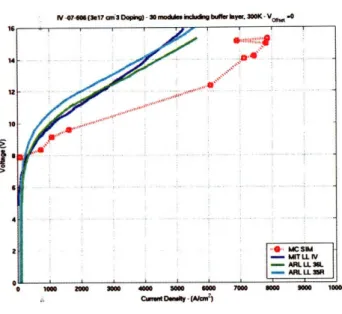
3-2 Two Module Bandstructure of Miniband QCL structure from Razeghi 4.7 Pm [3] 54 3-3 Monte Carlo simulated IV versus experimental IV . ... 55
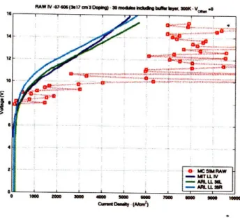
3-4 Raw simulated IV curve ... .... ... . 56
3-5 Example of Anticrossed state ... 56
3-6 Gain versus Current Density for MIT 606 Series . ... 57
3-7 Subband Populations versus Simulation Time. Blue = Upper Lasing Level, Red = Lower Lasing Level ... 57
3-8 Band Diagram of Two Phonon Injectorless Design [2] . ... 58
3-9 Monte Carlo Simulated IV versus Temperature compared to Experimental Data 59 3-10 Injectorless Gain versus Current Density for various temperatures ... 60
3-11 Current Density Threshold for Injectorless Design . ... 60
3-12 Current Density Threshold for Injectorless Design . ... 61
4-1 Experimental Setup ... 63
4-3 MATLAB GPIB pulsed LIV Screen ... 65
4-4 Q CL M ount . . . .. . . . .. . . . 66
4-5 Vacuum Chamber from the Top ... 67
4-6 Front View of the Vacuum Chamber ... 67
4-7 TEC Cooler Setup ... 69
5-1 Band Diagram of MIT 674 Injectorless Design - Two Modules - Layer Thick-ness (A) 21/21/51/14/37/17/29/32. Layers start with a well and bold layers are doped 9 x 1016cm-3 . Material Composition: Ino. 66Gao.34As/ Ino.30Alo.oAs.0 Designed Bias is 158 kV/cm . ... ... 71
5-2 Anticrossings Strengths ... 74
5-3 Parasitic Anticrossing Strengths ... 74
5-4 Band Diagram of MIT LL Injectorless Design 2 - Two Modules - Layer Thick-ness (A) 32/24/19/55/13/41/15/32. Layers start with a well and bold layers are doped 2 x 1017cm- 3. Material Composition: Ino. 65Gao.35As/ Ino.30Alo.70As. Designed Bias is 148 kV/cm. ... 75
5-5 Parasitic Anticrossing Strengths ... 77
5-6 Processed Ridge Structures ... ... 80
6-1 599 EL Spectrum - Doping 1 x 1017cm3, FWHM = 23 meV ... 84
6-2 605 EL Spectrum - Doping 2 x 101cm3, FWHM = 37 meV . ... 84
6-3 605 Lasing Spectra - Doping 2 x 1017cm3 . . . 86
6-4 606 CW Lasing Spectra - Doping 3 x 1017cm3 . . . . . . 86
6-5 Amplified Spontaneous Emission Spectra for various biases - bias is increasing from bottom to top ... ... 89
6-6 Fourier Transform of ASE -Interferogram of raw data . ... 90
6-7 Gain versus Bias ... 92
6-8 Gain Versus Current for 07-605 Sample, 2mm long, 8 um . ... 92
6-9 Filter Window for reprocessing the Interferogram . .... ... .... 93
6-10 Results from Filtered Interferogram ... 94
6-11 LIV from 08-674b5 Bar 5 at 77K. Blue represents IV, Red represents LI ... 95
6-13 Spectrum from 08-674b5 Bar 5 at 77K ... 96 6-14 IV for 08-696c5 - 77K and 300K, 250 ,im disc structures, 4 x 1017cm-3 Doping 98 6-15 IV for 08-697c5 - 77K and 300K, 250 Im disc structures, 2 x 1017cm-3Doping 98
List of Tables
Basis Functions U,o(r)H1 = (uno(r)lHlumo(r))
H2 = (Uno(r)IHIumo(r))
H1= (uno(r)lHlumo(r))
Table of Material Parameters ... Bowing Parameters for InGaAs, InA1As ...
Various InGaAs Material Parameters after Interpolation . . . Various InA1As Material Parameters after Interpolation . . . .
Various Conduction Band Offsets - Quoted values from papers, from Model Solid Theory ...
Simulation Parameters [3] ...
Simulation Parameters Injectorless 6.7 Im [2] . . . . Energy Spacing ...
LO phonon scattering times. Tjifetimes = E 1/Ti . . . Dipole Moment ...
Simulation Parameters ...
Anticrossings Strengths . . . .
Parasitic Anticrossings Strengths - Tlifetime = lps, Th
Energy Spacing ...
LO phonon scattering times. Tidfetimes = E 1/Ti .
Dipole Moment ... Simulation Parameters . . . . . . • . . . . . . .l. . 10 f . . . . . .. . . . .. . . .. . 77 2.1 2.2 2.3 2.4 3.1 3.2 3.3 3.4 3.5 3.6 3.7 5.1 5.2 5.3 5.4 5.5 5.6 5.7 5.8 5.9 5.10 Calculated • . •. ° °. . values
...
...
...
...
0 . . . . . 5.11 Anticrossings Strengths5.12 Parasitic Anticrossings Strengths - Tlifetime = lps, TII = 100fs . ... 77
5.13 Growth Sheet . . .. . . . . .. . . . .. . . . .. .. . 80 5.14 W all Plug Efficiency Metric ... 82
Chapter 1
Introduction
Quantum Cascade Lasers (QCL) since their invention in 1994 have become the dominant source for compact, robust, tunable, high powered lasers in the mid-infrared (Mid-IR) spanning 3 to 20
Pm [4]. Current QCL performance ranges from 300-400K and CW power of 1.6 W [5]. The main
driving factors behind these squrces are numerous sensing applications in the Mid-IR. Chemical spectroscopy and trace gas sensing are the most common areas due to strong spectroscopic signatures in the Mid-IR caused by molecular vibrational resonances. Furthermore, due to low atmospheric absorption between 3 to 5 pm work is being done on developing communication links that would be stable irrespective of weather conditions as well as infrared counter measures. These applications for a portable Mid-IR laser source motivate the need for an efficient lasing source, in order to reduce the need for excessive cooling and power supplies. Currently, the maximum wall plug efficiency (WPE) is only 12 % WPE under CW conditions [5]; however the desired WPE for these applications would ideally be 25-50 %. Therefore, there is still a lot of work necessary to achieve these performance levels. The quantum cascade laser is a powerful example of band structure engineering. The original concept for a QCL dated back to 1971 by Kazarinov and Suris [6]. However, it was not until 1994 that the concept was first demonstrated. With the development of heterostructure quantum wells, electronic states could be engineered into a laser structure. Unlike traditional interband semiconductor lasers which rely on the intrinsic properties of the materials to define the wavelength, QCL's emission wavelength can be engineered by varying the thickness of the quantum wells. This flexibility means with a given material system such as InGaAs/InA1As various wavelength lasers can be made. Designing these quantum wells has yielded many various configurations and design paradigms, one of which the
"injectorless" will be the primary focus of this work. [1].
A Quantum Cascade Laser (QCL) is a series of quantum wells grown in a periodic manner that create a cascaded structure of energy states when a voltage bias is applied. Semiconductors when grown on top of different semiconductors form heterojunction quantum wells. These quan-tum wells provide confinement for electrons. The appropriate energy levels and confined states can solved by using Effective Mass theory to simplify the problem down to a 1-D Schroedinger equation. Solving for the quantized states in these heterostructures is similar to solving "particle in a box"-like problems as shown in the energy band diagram in figure 1-1. Electrons sit in these
Figure 1-1: Two Phonon Design with miniband injector [1]
energy states and with an applied electric field, cause current to pass through these devices. In figure 1-1, an electric field has been applied to bring levels (g) and (4) into alignment. Electrons in (g) tunnel into level (4); the rate of tunneling is controlled by the thickness of the injection bar-rier. Electrons in level (4) due to a strong coupling with light fall to level (3) and emit a photon. Electrons in level (3) can also absorb a photon and become excited into level (4). Therefore, for proper lasing to occur, we require a population inversion between levels (3) and (4). To achieve this, electrons in level (3) need to scatter quickly to lower levels (2) and (1). By designing the level pairs (3),(2) and (2),(1) to each be resonant with a Polar Longitudinal Phonon or lattice vibration, electrons in level (3) can rapidly scatter into lower states. Level (1) was introduced to prevent thermally excited electrons in (2) from backscattering into (3). Electrons then transit
from one module to the next through a quasi-continuum of states or miniband. This process is repeated for each module, typically 30-40 modules; electrons are recycled allowing one electron to emit one photon per module. The two-phonon design with miniband presented here has so far produced some of the higihest wall plug efficiencies and CW performance.
It was originally thought that a miniband was necessary for proper device operation and stable current injection. However, recently a series of papers have explored the possibility of an "injectorless" design [7] [8] [2]. Essentially, these designs remove the miniband and electrons from the active region are directly injected into the next. These injectorless designs have already
5 4 3 2 1 5 4 3 2
1
Figure 1-2: Injectorless Design [2]
demonstrated room temperature CW performance and some of the lowest threshold operation S0.150 kA/cm2 [2] at 77K; however, the performance drops at 300K. Furthermore, these in-jectorless designs have some promising benefits for higher WPE that have not yet been fully explored. This will be covered in chapter 2, when deriving the metrics responsible for WPE.
Therefore, the work presented here will focus on the injectorless design as an approach for higher WPE. This includes:
1. Theory -Fundamentals of effective mass theorem, nonparabolicity, spontaneous and
stim-ulated emission, nonradiative scattering, resonant tunneling, and WPE.
3. Experimental Setup - Design and construction of device characterization Software and Hardware
4. Designs - New Designs for Injectorless Structure
5. Measurements - Preliminary measurements of samples as well and Fourier Transform
Chapter 2
Theory
The theory behind quantum cascade lasers involves understanding the underlying electron trans-port and scattering in semiconductors, as well as, how light and matter interact. Therefore, we will focus initially on describing electrons in solids and heterostructures through envelope for-malism. This formalism simplifies the microscopic details of a system and allows electrons to be described by a simple envelope function. These envelope functions will be important later on for computing electron scattering as well as spontaneous and stimulated emission.
-.-2.1
k. -i Hamiltonian
In order to describe an electron in a solid, we must first derive the bandstructure in a semi-conductor. This derivation for the K.P. Hamiltonian follows from references [9] [10]. For a semiconductor we can write down the time-independent Hamiltonian for the system.
+ V(r) + h4 (a x VV)-p (r) = EV)(r) (2.1)
2mo
4mgc2V r + nai) = V (r) (2.2)
In equation (2.1), the third term describes the spin-orbit coupling term. Because we have assumed a periodic potential, the solution O(r) to (2.1) takes the form of a Bloch wavefunction (2.3).
where N is a normalization coefficient. The Bloch wavefunction is labeled by n and k, the electronic band and crystal momentum respectively. Assuming this bloch form for the wavefunction we can obtain equation (2.4) by substituting (2.3) into-(2.1)
p2
hh2
k2 hk
h
EnkUk V(r) (a VV) + + - + X VV nk (2.4)
2mo 4m2c2 2mo mo 4moc2
As is often the case, we are concerned about describing electrons at high symmetry points such as the r or k = 0. In order to solve (2.4) we can take a perturbative approach by expressing the solutions in terms of known solutions at k = 0.
Assume the unperturbed hamiltonian for k = 0 does not include effects due to spin orbit coupling.
Ho = + V(r) (2.5)
2mo
Houno - EnoUno (2.6)
Therefore uno, assuming a tight binding method, represents S and P atomic orbitals centered on the periodic lattice sites. Adding back the spin-orbit coupling terms as a perturbation allows us to use a finite basis expansion to expand the solution in terms of these atomic orbital terms.
h h2 h2
H = Ho + k p + (VV x k) -a + (VV x p) a (2.7)
mo 4mTc 2 4m2c2
E'k = Enk -
(2.8)
2mo
In most cases, kl << pl, so we drop the third term in H.
H Ho k -p + (VV p) - a (2.9)
mo 4m0c2
Using the complete basis centered at F we can write our full solution as a sum of the k = 0 states.
Unk(r) = alt(k)uzo(r) (2.10)
where 1 is the electronic bands at k = 0 and at(k) represents the weighting coefficients for the various basis states.
Table 2.1: Basis Functions uo(r)
Where in Table 2.1, we have defined the following terms. 1 3 3
4(PY4m
c22 19P (2.11) (2.12) V Pa )
Px)
Given our full Hamiltonian including perturbation and applying a finite basis expansion, we can solve for the weighting coefficients.
(2.13)
S[(uno(r)IHIumo(r))
- Enk] an(k) = 0m=1
Hnm = (uno(r) Hlumo(r)) =
H
1
H2
H2 H1
Where the Kane parameter is P = -i-(SIpi Pi) C (x, y, z) and k+ = '(kx + ik). These matrix elements can be computed by applying symmetry and parity properties of the Bloch
Table 2.3: H2= (uo(r)lH umo(r)) U50 U60 U7 0 U8 0
u1o
0
-
Pk_
0
-
Pk_
U2 0 6Pk 0 0 0 U3o 0 0 0 0 U4 0 / Pk_ 0 0 0 atomic orbitals [10].Fully solving the 8x8 K.P. Hamiltonian in equation (2.13) will yield the energy dispersion (E vs. k) relationship for the conduction, light, heavy hole, and split off bands. This provides a method for estimating the band structure of a material by utilizing known solutions around a fixed k point. Furthermore the microscopic properties of the material have been absorbed into the Kane Parameter and Spin Orbit Split Off, which can be estimated experimentally.
Because we are dealing with bulk materials, we can choose to an orientation where k//J//z. This choice of direction, greatly simplifies the math due to the decoupling of many of the basis states from each other. Table 2.4 shows the reduced k.p matrix.
The characteristic equation for the eigenvalues of this matrix are E'k = -Eg or
(Elk)(Enk + E,)(Enk + E9 + A) = k2P2(E'k + Eg + ) (2.14)
while no closed form expression exists for the eigenvalues, we can solve for the conduction band energy dispersion by assuming that Ik is located near the r pt, so we can look at the lower
Table 2.4: HI = (uno(r)IHlumo(r))
i
10
U
20J30
U40
uio
0
-
Pko 0
Pk
U20 - Pkz -Eg 0 0 uso 0 0 -E, 0 U4o FPkz 0 0 -E -Aorder terms of Ec = 0 + e(k2).
h2
k
2[
1 4P2 2P21
2kk
2Eck = Ec(k) = -2 • + 2 + 2(E + ) (2.15) 2 mo 3hEg2E (E+ A) 2m
Looking at the 4 possible solution, near the band edge, we see that the heavy hole states decouple and are not dependent on k. In order to include the curvature of the heavy hole, one needs to consider inclusion of remote band effects, which are derived by Bastard [9]. Even though the k.p. hamiltonian solves for the bulk bandstructure of semiconductor, we will show shortly its use for describing electrons in heterostructure quantum wells.
2.2
Envelope Approximation
For devices of interest, we are concerned with describing electronic waveforms of semiconductor heterostructures. Heterostructures are made from growing layers of different materials on top of one another. Due to differences in band alignments between materials, quantum wells and thus electronic confinement are created. By assuming that the scale of variation of the materials is greater than the actual atomic variation, an envelope approximation can be used to greatly simplify the problem. This envelope approximation is otherwise known as the Effective Mass Theorem [9] [10]. Therefore, the solution for the various bound states and energy values can be reduced to solving equation (2.16), where k --+ iV.
[ Hnm(k = -iV)Fm(r) + Fn(r)U(r)] = EF(r) (2.16)
Where Fn(r) represents the envelope function for band (n), and U(r) is the slowly varying potential. For most cases, our perturbation is due to the various band offsets in the growth direction. Therefore, let us limit U(r) to U(z). While solving equation (2.16) yields an accurate solution, this equation can be written in its more common form for the conduction band, by utilizing equation (2.13)
[E,(k = -iV) + U(z)]Fn(r) = EF,(r) " (2.17)
Using equation (2.15), we can rewrite equation (2.17).
-&2V2_-h2 _
'F- FV(r) + Vz VzF(r) + U(z)Fe(r) = EFe(r) (2.18)
2m (z) + ()) .
From equation (2.18) the envelope wavefunction takes on the form
F(r) = eik_-rI F(z) (2.19)
Substituting equation (2.19) into (2.18), we get
h2k2 -h2 1
'Fe(z)
+
Vz
VzF (z) + U(z)Fc(z) = EFe(z)
(2.20)
2mC(z) 2 m (z)
Equation (2.20) couples k with z, which complicates the problem. For simplicity, we assume parabolic subbands in k with the effective mass of the well.
-(2 1h 2k2)F
V2 Zm(z) VzF(z) + U(z)Fc(z) = E + Fe(z) (2.21)
Equation (2.21) takes on the simplified form of a 1-D Schroedinger Equation, where the micro-scopic properties of the material are grouped into the effective mass parameter. This equation assumes parabolic bands close to the band minimum; however, for most Mid-IR device, this is not the case. Therefore, we must introduce higher order effects to deal with non-parabolic bands A common approach involves using an energy dependent effective mass, which can be derived explicitly by solving the full k.p. Hamiltonian in equation (2.16).
ignore the free electron terms 2
k2 , which contribute terms on the order of (Ec - Elh,so)/Ep << 1.
Therefore if we assume k E (0, 0, kz) we arrive at the set of equations
Ec(z)
2Pkz
-
VPk
(
Fe(z)
Fe(z)
Pkz Elh(z) 0 Flh(z) = E Flh(z)
- Pkz
0
E,,(z)
F
8o(z)
F,,(z)
Implicitly, the Bloch components of the different materials are taken to be equal. This is because the Kane Parameter (P) does not change significantly between the well and the barrier material. The only change between the well and the barrier is due to different energy alignments of the conduction, light-hole and split off bands. We can write the closed form solution by explicitly cross eliminating the light hole and split off envelope functions from the first row of k.p. matrix, which yields
1
Pz 2m(E zF) + E,(z)Fe = EFe (2.22)
2m(E, z)
m(E, z) = moE- Ev(z) (2.23)
Ep
Where E,(z) = (2Elh(Z) + Eso(z))/3 is the effective valence band and P = iE- [11]. We can rewrite equation (2.23) in terms of conduction band effective mass in a material m = mo(Ec - E,)/Ep.
m(E, z) = m (z) I + E - Ec(z)
As for the appropriate boundary conditions, we assume the continuity of
1. Fe
2. 1 dFa
m*(E,z) dz
Figure (2-1) shows the importance of nonparabolicity away from the conduction band edge for the upper lasing level.
Number of nodes in x grid = 1000
x 10
Figure 2-1: Effect of Nonparabolicity on QCL energy levels. Dotted lines are without non-parabolicity, solid lines are with nonparabolicity
2.3
Intersubband radiative transitions and gain
Given the envelope wavefunction for an electron in a quantum well, we can now describe optical processes for lasers such as spontaneous and stimulated emission. We first need to derive the
interaction hamiltonian due to light. From the Lorentz Force Law, we know
F = q(E +v x B) (2.24)
(2.25)
(2.26) 0A E = -V -atB = V
xA
Where, B and E are the magnetic and electric fields, and A and ¢ are the magnetic vector potential and electric scalar potential. The Lagrangian is defined
Where KE is the kinetic energy, and U is the potential energy. Therefore, under this definition we can also define the force in terms of U.
Fx U+ +(2.28)d= ( U
The solution to this equation in terms of the scalar and vector potentials is
U = q(0 - v -A) (2.29)
Therefore, classically we can write out explicitly the Lagrangian in terms of position and velocity.
1
L(r, v) = -mv2 - q(¢ - v -A) (2.30)
2
Furthermore, we can express velocity in terms of canonical momentum.
8L(r, v) S-OL(r, v) = mvx + qAx (2.31)
vx(
1v = - (p
-
qA)
(2.32)
mUpon substitution of equation (2.32) into (2.30), we can define a constant of motion
1
E = q + 1(p - qA)
2m
2 (2.33)Since we are considering the interaction of light and electron in a solid, we will assume the mass is the effective mass (m*). We can also write the quantum mechanical hamiltonian by replacing variables with their analogous quantum mechanical operators. If we assume a Coulomb Gauge V -A = 0, the interaction hamiltonian is
Hint = - A -p (2.34)
m*
Where A and p are operators now. To compute optical transitions we apply the results of time-dependent perturbation theory and Fermi's Golden Rule.
2 (2.35)
Where in equation (2.35) the time oscillations of the field have already been accounted for in the interaction hamiltonian and are represented in the delta function. (i) and (f) represent the full initial and final wavefunction states of the system. This explicitly includes the envelope functions, Bloch functions of the electrons, as well as the photon field. The description of the photon fields is the result of second quantization, which is derived in [12].
ji) = |ki)Inq,,) (2.36)
If)
=
Ik)lmq,a) (2.37)1
Ik,) = uv,(r) exp(ik± -rl)Fi(z) (2.38)
n and m represent the photon number in the cavity with polarization a and in mode q, and
u, (r) represents the initial bloch wavefunction for band (v), and S is the normalization factor.
Utilizing the results from second quantization of the field we can express A in terms of lowering and raising operators that act only on the photon number.
A
=[qaq,
etiqr
+
aqe-i.r]
(2.39)
Substituting equation (2.39) into the matrix element of Fermi's Golden Rule, we get
(ijHintlf)
=
m*3q 2wV
q
h
6m
-l,nq,a(kie|q,a- pe
q.r kf)+
q h ir
m* 2EWqV mqa +
16mq,,+1,nq,r]j(kiIq,a -pe-i.jkf)
Given that q = j, where A is on the order of 10plm, the wavefunction and r vary on the order
of order of nanometers, therefore, we can approximate q -r P 0
(iIHintlf) -= m*q / 6m,,,-l1nq,,,q,a * (kilplkf) +
We have computed the photon part of the wavefunction; however, we still need to compute the spatial component of the wavefunction, which includes the entire wavefunction including the envelope and bloch wavefunctions.
(klle" plkf) = q,,
]
d3ru*(r)--exp(-ik() " r±)F*(z)puv,(r) exp(ik) -r2)Ff(z)= eq,,. dru* (r)- 1exp(-ik() -r±)F*(z)-expp(ikf) r±)Ff(z)pu,(r) +
(r)1 ex (i -)Fj*(z)u,( r 1 en(ik) -Lr)Ff(z)
Due to the periodicity and rapid variation of the bloch wavefunctions compared to the slowly varying envelope function, we can approximate the integrals
(kzlplkf) - (uv,(r)Ipjuv,(r)) dr exp(-ik -•) r±)*(z) Sexp(ik) -r )Ff(z) +
(U,(r)|(r)) d3r-exp(-ik(') -r )Fi*(z)p exp(ik' r)F(z)
Reintroducing the dot product of the polarization and the momentum we get
(kil|q, -plkf) = (uv,(r)l q,. pluv,(r)) 6c(k~) - kf))(F,(z)IFf(z)) + (2.40)
(u
- k¶ )(-ihevk + -iheyku)(Fi(z)lFf(z)) + (F(z)lez
plFf(z))
(2.41)
So the first term in equation (2.41) represents an interband transition for example between conduction and valence band. Furthermore, in an optical transition, the transverse k is conserved between transitions. For the case relevant to intraband transitions, i.e. bound conduction band states, the envelope functions between different states are orthogonal due to the hamiltonian. This yields the famous intersubband selection rule, where the polarization can only be in the z or growth direction.
Furthermore by applying the commutation relation, we can write the momentum matrix element in a more familiar form in terms of a dipole moment.
PZ
h [Ho, z] =
- m*im*
(Fi (z) pz F(z)) =
hi
(Ef - Ei)(Fi(z) z IFf(z))(2.43)
(2.44)
However, when using equation (2.42) one has to pay careful attention to the form of the operator and envelope function used. When including non parabolicity, the conduction envelope functions are not guaranteed to be orthonormal since the full solution to the Hamiltonian must take into account the sum of all the envelope functions and Bloch wavefunctions from all the bands. We will discuss this complication in the following section.2.3.1
Dipole Moment with nonparabolicity
Due to nonparabolicity, we need to consider the envelope functions bands in order to properly compute the dipole matrix element [11].. Hamiltonian used to derive the envelope functions is
Ec(z)
- PkZ 513Pk, /Pkz Elh (z) 0 - Pk z 0E
8o(z)It
Fec
FIh
Fso
=E
from the various valence The exact definition and
Fc
Flh
Fso
the Pz operator is actually the off-axis matrix elements, k - p in our original hamiltonian.
Pz=
0
O
- VPmo SPmo
which originally were the result of the
VPmo - APmo
0 0
0 0
We can express the light hole and split off envelope functions in terms of the conduction band envelope functions.
1••PPPzFC = (E - Eso(z)) Fo (2.46)
The full expression for the optical matrix elements is
0 Pmo - /Pmo Fcf)
( i(z)pzlP0f(Z)) = Fj) F(i)
F
)
-Pmo 0 0 F1Pm 0
o/Pmo o
0I
F/ )9Fortunately, we can write a closed form expression for the optical matrix element, without having to compute all the valence envelope functions.
1
10
Mn
MO_)
(Obi(z) PZOf (z)) =mo mo pF+
IF')
(2.47)2 m(Ei, z) m•(Ef , z) c
In addition, the total wavefunction is normalized to one, not just the conduction band compo-nent. Therefore, the proper normalization is
2
JPJ2/m2 1 p2/ 2(~c|1 +
p [E(, - ELh(z)]32P
•
+ 1+-P
[E(,) - E
Ppc)=
0Pz
1(2.48)
8 0
o()]2
According to Sirtori [11] the use of standard dipole moment for computation is still valid and commonly overestimates ; 5-10 percent. Finally, we can write the total optical scattering rate for emission as
Weis
r
q2
qo, + 1) e2p(i-f) 26(Ef - E, + hWq) (2.49)W ems icV-EC+h) i = rq2w(mq, + 1) e(i-f)2(Ef - E + ) (2.50)25
Where p(--f) and z( i- ' ) are computed normally or by taking into account nonparabolicity by equation (2.47).
2.3.2
Spontaneous Emission Lifetime
From equation (2.50), we can define two individual rates, one that is dependent on the photon number (m) in the cavity and one that is independent. The former is stimulated emission, the
latter is spontaneous emission. Electrons can automatically emit a photon given a certain proba-bility. However, our previous derivation assumes emission into a specific mode and polarization. To compute the total rate, we need to sum the total rates into all available modes (q) and polarizations (a).
Wi - q2 e |z(i--f)126(E - Ei + hwq) (2.51)
If we assume box resonator, then in q space the available states available are uniformly spaced discrete points. The density of q states is 1/(27r/L)3. In spherical coordinates.
q d3= q Vq2 sin OdqdOdq (2.52)
p(q)d3q 87r3/V 873 (2.=5/2)
ot = Wlmode (q)p(q)d3q = • (i- f) 2 qeq 2 sin 06(E
-Ei + hWq)dqdOdq
(2.53)
Assume we integrate such that one polarization is always normal to the z axis, and the other polarization lies in between the z and q axis. Therefore, e2 = sin2 2W.(Sp) P 3
q
e
2 1 Z ) 12 zi-+f 2 3ftot - Wifmode(q)p(q)dq =c z(i-*f) 2 Swqqin3 O(Ef - Ei + hWq)dqdOd8
(2.54) The result is
2 3
ot 3h 4c (i-- )12(Ei- Ef)3 (2.55)
WsP) o e 2n I z(i-+f) 2W3 (2.56)
= wil (2.56)
In the Mid-IR the total spontaneous emission rate at 5 ,m is often on the order of Tr-f r 20 ns.
2.3.3
Stimulated Emission
In the case of stimulated emission, on the other hand, we compute the emission rate into a specific mode. For most laser cavities, there are usually one or two low loss modes where emitted photons can exist long enough for the stimulated emission rate to increase. This feedback loop between
emitted photons generating more photons is the basic concept behind a laser.
W irq 2 Wqm eq2m z(i-f) 126(Ef - E, + wq) (2.57)
However, due to relations with uncertainty, the energy level is not exactly discrete, but rather distributed over a range of energies. So often the delta function is replaced with a normalized lineshape function g(E)dE = -g(v)dE. Therefore,
Wf = / rqm2wm' 21z(If'26(Ef - E, + wq) hg(v)dE (2.58)
w
8
, =
2qwqm,e
2z(if) 2g(v)
(2.59)
Expressing the number of photons in the mode using the field strength
Cmq,crhWqa
I = cm, (2.60)
nV
Therefore, we can rewrite the expression as
X21
W.if
if
=- 87hwn2
g( ) (2.61)ant
The linewidth of the Lorentzian linewidth is determined from lifetime broadening [13]. However, there is a factor of 3 that is missing from equation (2.63), which accounts for the fact that for intersubband transitions, unlike atomic medium, all the dipole moments are aligned [14]. Therefore, we have 3A21 W. = 81rhw2t1 g(/) (2.62) 3A21 Av/2r (263) if = 8rhwn2t9t (v - vo)2 + Av/2)2 1 1 2 2rAv = Aw = -- + - + (2.64)
The linewidth factor can be understood by remembering that a finite exponential decay in time domain, when fourier transformed, yields a Lorentzian in frequency domain, whose width is determined by the decay. Where T2* represents the pure dephasing rate and ri and 7f are state
lifetimes. For a more complete derivation of linewidth broadening due to coherent collection of classical oscillators see Siegman [13]. This linewidth broadening, as we will see when computing intersubband gain is critical and can be measured from the linewidth of spontaneous emission, which in the Mid-IR is • 25 meV.
2.3.4
Intersubband Gain
Due to stimulated emission, photons emitted into a cavity mode, increase the intensity of that mode leading to gain or amplification. To calculate the gain, we compute the number of extra photons generated along the axis of the cavity. The power flux (W/m 2) of a wave in medium is related to the time average poytning vector.
1
P = (E x H) = -EoneEo (2.65)
We assume our waveguide has transverse dimensions of w and L. Therefore, the photon flux normal to the direction of propagation is
1
1
1Ž= coneE
2
0 oAw
wL (2.66)Therefore, the photon flux over a length dy along the direction of propagation is therefore
d1 = W(2t)n
2wdy
-
W(2t)•1wdy
(2.67)
Where n2, and nl are the sheet densities of electrons in level 2 and 1. We also note that the
stimulated emission and absorption rates are equal. We define G as the increase in number of photons divided by the total number of photons present. [15]
d@/dy = W(1t ) Aw 3A2I tiww
G = dPd- Wt21 ) ( - n1) n 2 - r1)9(v) S2IwL 8~(n2 87wn2tspont Iw 3A2 1 C = -(n 2 - nl)g(v) 8n 2t spont L
G
=
31
e2 (if)2 f 2 -n1)g() 2n coh VFor simplicity, we have assumed a low population density, such that we can assume that the final states of the electrons are free and available. We can also express the peak gain when v = vo
G( v) - e2z(i-f) 2wf (n2 - n1) 2
G(v = L)= (2.68)
2n L - n) 2 (269)
G(v = vo) =
nfoc
L AE
(2.69)Where AE is the linewidth measured from spontaneous emission. However, the key factor is
that the gain of a system is positive only when n2 > nl, or when one has a population inversion.
2.3.5
Nonradiative Scattering and Transitions
In quantum cascade lasers, population inversion is achieved by engineering the scattering rates and subband lifetimes. These subband and electronic populations are primarily controlled by nonradiative scattering mechanisms. There are a variety of nonradiative scattering mechanisms that are present in controlling electron transport including e-e scattering, acoustic phonon, electron impurity etc. For more detailed deviation and computational implementation for each of these scattering mechanisms see reference [16]. The mechanism that we will focus on primarily is polar longitudinal optical phonon scattering. This mechanism has a flat energy dispersion and for InGaAs is . 34 meV. When subband levels are resonant with a LO phonon, the nonradiative scattering mechanism occurs on the order of 0.2 ps, which provides the main depopulation mechanism for various double phonon QCL designs. To compute the scattering rate due to LO phonon scattering we must again use Fermi's Golden Rule, with Hint is assumed to be [17]
H = C
[ajei3.r
+ ate-3.r
(2.70)
=
0
hwLoe
2(
1 1(2.71)
2V /32 E"o EDC
As was the case for optical tr'ansitions, we can quantize the phonon motion, which assumes a certain phonon number, which are affected by the raising and lowering operators in equation
(2.70)
ULO
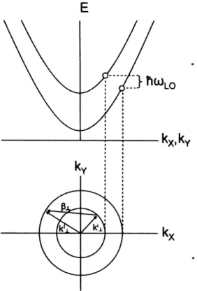
Figure 2-2: Diagram of LO phonon scattering between two parabolic subbands.
Ii) = Iki, np)
If) =
Ikf,mm
)
Iki)
(2.73) (2.74) (2.75) 1 ik()-r=
(v)(V)-
e
I F(z)
Therefore the matrix element of Fermi's Golden Rule for just the case of emission or absorption is
= C2 (m +
= C2 (mf
= C2(m
fd ru (r) 1eik •r F,* (z)e-ip.ru(r) 1 eikT )
[J r
v,-S
-f k
r
1 2 1 2•F,(z)]I
d3re -ikJ2rI F* (z)e-i3"reik )'rIF(z)]F
[ F*(z)-izzFi(z)dz] 2
The integration over the k ensures transverse momentum conservation.
27 hwLoe2 h 2V
EDC
)00 + 1 2 2/ 1x
O'[ + P,2I(i|Hlf)
12 WLOi- f(Utiv,
(r
i(r))
[JF*(z)e-iazzFf(z)dz]
26k',k(,16(Ef
- E
±
rh)
In order to compute the total scattering rate out of ki we must sum over all possible allowed final states kf and allowed (,3_, 0z). For simplicity let us look at the integration over fz since it does not have any restrictions in terms of energy and momentum.
B4f (P0) = Jdfz F1*(z)e-izF(z)dzJ Fi(zi)eiz' F(z')dz (2.76)
=
JF(z)F(z)dzJ
F(z')Ff(z')dzdJ
z p1
.e-iz(z-z')
(2.77)
Fortunately, we can use a fourier transform pair to evaluate the integral Oz on the right.
Bi--.f(Oz) = fr*(z)Fi(z)dz Fi(z')Fr*(z')dz'e- id±lz- z 'I 1 (2.78)
In order to integrate over the final states with allowed 3±, we can combine the conditions for energy and momentum conservation into
3p
= k, + k2 - 2kikf cos 0
(2.79)
2 2m*(Afi T hWLO)
k
=
kh
+
(2.80)
A•, = Ef(k = 0) - E
2(k = 0)
(2.81)
Therefore, to satisfy energy and momentum conservation, we can integrate over 0, which is the angle between vectors ki and kf.
wLO(k ) 27r hWLoe2 1 1 1 1 )f
2
Wrok
= h 2V EDC + 2 + 0oo dOUB-_.f (3) (2.82)
h 2V C 0 DC 22
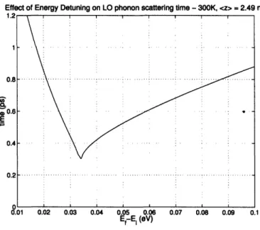
To account for phonon statistics we can assume Bose Einstein distribution functions that are in equilibrium with the lattice temperature. We have also included figure 2-3 to show the effects of detuning the subband separation given fixed wavefunctions.
m= (2.83)
Effect of Energy Detuning on LO phonon scattering time - 300K, <z> = 2.49 nm
E,-E1(eV)
Figure 2-3: Effect of Detuning between subbands versus scattering time
2.4
Resonant Tunneling
So far transport of electrons has assumed a coherent process where electrons due to specific scattering mechanisms can scatter from one subband to another. However, it has been shown that this coherent process of transport, at least between modules, may not be entirely accurate. In quantum cascade lasers describing the transport between modules is often treated using resonant tunneling [18]. Experimentally this is shown through the strong dependence of injection barrier thickness to current density. For coherent transport when two levels align, the wavefunction assumes a spatially delocalized state across the barrier and thus has some large spatial overlap with subbands in the next module. Therefore the injection barrier would have little affect on the total current passing through the barrier. Furthermore, dephasing due to transport accross a barrier is critical for QCL performance. Modeling of dephasing can most easily be done through Density Matrix Formalism.
2.4.1
Density Matrix Formalism
For an arbitrary electron wavefunction
10)
= EcnIq|)
(2.84)
38
Where 0, are the basis states of the Hamiltonian. If one were to compute the expectation value of an operator then
(0|o|4) = EC
cmcn (•mlO|l
) = ••C~CnOmn
(2.85)
m n m n
Let us define the density operator p and density matrix P,,m
p = |I)()| = • c•c2cmj•m)(On (2.86)
m n
Pnm = (¢mIP•ln)
ccm
(2.87)
Pnm = (mlIPk1n) = (cncm) (2.88)
Therefore, for a single particle we can express the wavefunction in this density matrix formalism. However, for our purpose the density matrix through averaging many different single density ma-trices can represent an ensemble average, which allows us to model large collections of electrons at once assuming some mean behavior, which is the true strength of this formalism. Therefore, the expression for the expectation can be written as
(0) = E P*mOmn = E PmnOmn
(2.89)
mn m n
Furthermore, the density matrix is Hermitian
Pnm = (OmlP10n)* = (c*cm)* = cmCn = Pmn (2.90)
By taking the time derivative of the density operator we arrive at the time evolution of the density matrix.
ih
=
iha
(
+
ihlp)
(2.91)ap
ih-L = H1'i)(|1 - I)(1IH = [p, H] (2.92)
For clarity, let us only consider a situation where we only have two basis states. Furthermore,
we have assumed our Htot = H + Hre,., where Hrei, includes phenomenological relaxation
terms of a Hamiltonian.
a
P11 P12(
P11 P12 H11 H1 2 0pat P21 P22 P21 P22 H21 H22 Ot relax
For the case relevant for resonant tunneling, assume initially we have two isolated quantum wells with a very thick barrier. The initial basis states would naturally be |11) and
I02),
which are localized states inside the well. Assume the Hamiltonian for a single well is Ho then the coupling between the two wells can be viewed as a perturbation AV, so the H = Ho + AV. Therefore,(H
0|H|
1) (0
21H10 2)
2 El 1) ( AV1 02) El -A0/2(
(21H|H 1)
(021H0
)
2(2
1)EV
-Ao/2
El
The eigenfunctions of this matrix now form delocalized states that are symmetric and antisym-metric which are separated in energy by their anticrossing strength A0. However, with QCL's two states can be brought into resonance through an applied electric field. Therefore assuming fixed anticrossing strength, we allow detuning, such that the diagonal elements of the matrix can differ.
H = -Ao/2 E2
Furthermore, it becomes clear that if an electron is originally in one of these localized basis states, that it is not a eigenfunction of the Hamiltonian and will undergo oscillations between the two basis states, thus allowing tunneling across the barrier. Density matrix formalism also allows the ability to add in ensemble parameters, such as population lifetimes and dephasing phenomenologically.
P22 P12
at relax P21 _ P22
For simplicity, we assume a infinite periodic lattice. We define a lifetime 7 as the lifetime of P22 where an electron relaxes from 2 into 1. We also define T1I as the dephasing relaxation time due
to loss of coherence between the two wavefunctions. If current is directly injected into level 2, then the steady state current density J = ~.2 If we solve equation (2.92) for p22 under the condition that P22 + P11 = 1 assuming a constant population, we can express the current in a
form similar to the one provided by Karzarinov and Sirus [6].
qNP22 QN( )2
J - 2 (q,)2 2 (2.93)
h2
1 +
I
+ )
7711This expression can be simplified for the case where the two energy levels are resonant.
Jmax qN 1I
(2.94)
2
1+
_
)
rTr
We can estimate 711 from homogeneous broadening of the linewidth similar to equation (2.64).
1 1 2
- - + - (2.95)
1 1
Aw = - - (2.96)
T2 71
For a linewidth on the order of 25-50 meV this corresponds to a dephasing rate a 100 fs. It should be noted that the measured emission linewidth is the transition within a well, where as the linewidth in question is the transport across a barrier, which one would expect to be broader; however, this is an unknown parameter in the system.
The resonant tunneling model provides a a figure of metric when designing optimal de-vice performance of a QCL. Following from [18], the optimal strong coupling regime, where
I•'A2
2T7-l> 1, is preferred such that
qN
Jmo = (2.97)
We see that the current is limited not by the tunneling rate, but by the lifetime r, which means more electrons are available for gain. Therefore in designing QCL's careful attention must be paid to the various anticrossing between levels to determine the injector coupling strength.
2.5
Rate Equations for QCL
After deriving optical and nonradiative scattering mechanisms, we can use rate equations to determine what parameters are important for population inversion. As is done with many laser systems we reduce the QCL down to a simple three level system [14] [19]. Through detailed
771
evr
e-7)
eV
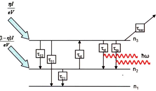
Figure 2-4: Diagram of Three Level system, assuming non unity injection efficiency
balance, we can write down the rate equations for the 3-D subband populations n3 and n2. We
can even keep track of the number of photons in a specific lasing cavity by including terms such as spontaneous and stimulated emission and absorption.
dn3 I -- n3 + (n2 - n3)mV n3 (2.98) dt eV Tsp t T3 dn2 _ (rq- 1)I Sn3 + (n3 - n2)mV n2 + n3 (2.99) dt eV p Tst 7T2 73 2 dm n3F (n3 - n2)FmV m - - + (2.100) dt Tsp Tst Tp
We assumed that current I is directly injected into level 3, V is the volume of the active region,
rq injection efficiency, T7 is the photon lifetime, F is the confinement factor.
1 = Vg(am + ) (2.101) VNmod V o= (2.102) 1 1 1 1 - = -- + + - (2.103) 73 732 73 1 Tesc 42
Where Vtot is the total cavity volume, and the n3 = n3
/L,,
and n2 = 2DIL,,. Now assumesteady state conditions.
l7I n3 (n2 - n3)mV n3 (2.104) + -- (2.104) eV Tp 7Tt 73 (n- 1)I n3 (n3 - n2)mV n2 n3 (2.105) =+ (2.105) eV 7sp t T2 T32
n3r
(n3 - n2)rmV
m
S(2.106) Tap TSt TpFor simplicity, we assume that 8,, > 7Tt and there are a large number of photons in the active region such that mV > 1. From equation (2.106)
7t 1
n3 - n2 = (2.107)
7, FV
For conditions above threshold, equation (2.107) demonstrates that the population inversion or gain clamps above threshold. We can solve equations (2.105) and (2.104) for the photon number (m) which is proportional to Light Intensity (L) assuming the fixed population inversion.
r7pr(073(1
-72/7
32)
- (1 - n7)72) (P Pth)(2.108)
m =(P - Pa) (2.108)72 + T
3(1
-
27
/T
32)
7Tt 1Pth =
TpVF(2.109)
7-r3(1 - 72/732) - (1 - )72(2.109) L = hwVpm (2.110) Tm Tm = (2.111) amVgWhere P = . Finally expressing equation (2.108) in terms of L, we can express the slope efficiency d or the amount of output power versus current.
dL = hwVp 7TF(7
pr
3(1 - T2/73 2) - (1 - r)72) (2.112)dl eV7m 72 + 73(1 - 72/T732)
dL hWNmod am (q7i3(1 - T2/732) - (1 - 19)T 2) dl e am + aw 72 + 73(1 - 72/T32)
(2.114)
2.5.1
Wall Plug Efficiency
Quantum cascade lasers have a distinctive advantage of being able to engineer the scattering mechanisms between levels by tailoring their energy separations as well as their wavefunctions. From equation (2.114), it is clear that the scattering times T3 2, 73, 72 are very important for high efficiency. For determining all the factors relevant for wall plug efficiency, Jerome Faist derives an expression for fundamental wall plug efficiency r)wp [20].
(I - lth)dL/dl
S= (IV- (2.115)
IV
Where V is the voltage to bias the device, I is the current, Ith is the threshold current. We can relate the parameters V for a specific device wavelength as
=V + Ai. Nmod (2.116)
qo
Where Aij is the voltage defect to bring the various levels into alignment beyond the necessary energy alignment separation between the upper and lower lasing state. Traditionally, depending on design this can vary from 70 meV for the injectorless to 120 meV for the traditional miniband designs. The voltage defect is due to the need for extra levels to provide depopulation. Using rate equation solutions, Faist simplified the wall plug efficiency down to a concise expression
2wp,max =
732
7327
73-72
- 1[
-1]
(2.117)
3=+-
T2/
1
+ Aj/ (
ST73(1 - 72/732) Ttrans m*W3T17Ii 1*=
h
Iz-fI
(2.119)
Jmax= nqo (2.120) TtransIt becomes very clear that the parameters that need to be optimized are v/g*»T > 1. Some of these parameters such as 7I1 are controlled by the growth and quality of the interfaces, which affect the linewidth. However, most of the other parameters in terms of lifetimes and voltage defects are parameters that are dependent on the design. Therefore, for this thesis we will further
Chapter 3
Simulations
Monte Carlo simulations were conducted for evaluating and studying various designs. Various simulation tools have been developed to study and model electron transport in quantum cascade structures. Most simulations for QCL's involve a semiclassical approach which is essentially a rate equation approach, where electrons in different subbands scatter into and out of different levels. A Monte Carlo approach is often taken to simulate ensemble electron behavior. These simulations were done on two designs to evaluate the performance of using these simulations for predicting the performance of new designs
3.1
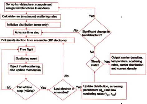
Monte Carlo
A common method for simulating electron transport in semiconductor devices is a Monte Carlo simulation. By following the Boltzman Transport Equations [17], electrons are assumed to be discrete particles with known momentum and energy. Electrons once inside a material can be subject to a variety of scattering mechanism such as optical phonon scattering, interface scatter-ing, impurity scattering etc. Each of these scattering mechanisms is assumed to be instantaneous and obey transverse momentum and energy conservation. The choice of scattering event is de-termined by the probability of each scattering mechanism. Allowing random events to choose the scattering event is where the simulation gets its name. The results of the simulation can yield information about final steady state populations, gain, electron temperatures, scattering rates, and current. The code used was developed by Hans Callebaut initially for simulating terahertz QCL. It was then modified slightly to take into account nonparabolicity for solving
mid-IR QCL structures.
Figure 3-1: Flow Chart for Monte Carlo Simulation
3.1.1
Free Flight
After computing the band structure, the Monte Carlo simulation must determine for each indi-vidual electron the time between scattering events. The probability distributions are determined by the relative strengths of the scattering rates computed using Fermi's Golden Rule. Further-more, each electron themselves is modeled with a specific k1 and subband (i).
t(k±, t) = ( (3.1)
m m(k ,-t)
Where m is the scattering mechanism and F is the total scattering rate. For simplicity, we assume Pi(k±, t) = Fo [17]. Electrons in the system are assumed to undergo free flight until a scattering mechanism is chosen. If we define ncf as the number of electrons which have not undergone a collision since time t=O, then assuming a scattering rate of 0o,
dntf = -roncf (3.2) dt n ef (t) e -rot -(3.3) ncf (0)
Equation (3.3) defines the probability that an electron has not scattered until time t. Therefore since Fo is the number of electrons scattering per second, we know that the the number of0 electrons that scatter in time interval dt is Fodt. The probability that an electron undergoes its first scattering between t and dt is the multiplication of the probability it has not scattered until time t and the probability of scattering in time interval dt.
P(t)dt = Foe-rotdt (3.4)
For computational reasons, we would like to map the probability distribution P(t) onto a uniform probability distribution P(r) P(r)
orc
dr = P(t)dt dr = poe-rotdt dr = Foe-rotdt(3.5)
(3.6)(3.7)
Where solving equation (3.7) is a simple map between a uniform probability distribution (re) and a time duration for free flight (t,).1
t= = - n(1 - r,)
F0 :
(3.8)
This assumption is of course assumes a constant scattering rate; however, this can be artificially introduced into the Monte Carlo simulation by introducing a fictitious self-scattering event.
self(k-, t)
=
Fo
-
Fr(kl,
t)
(3.9)This self scattering event, if chosen, does not change an electrons energy or momentum.
3.1.2
Choosing a Scattering Mechanism
Every particle due to its energy and momentum has its own unique probability of scattering. The process for choosing which scattering mechanism an electron undergoes and the corresponding
![Figure 1-1: Two Phonon Design with miniband injector [1]](https://thumb-eu.123doks.com/thumbv2/123doknet/14687276.560473/16.918.296.601.372.670/figure-phonon-design-miniband-injector.webp)

![Figure 3-2: Two Module Bandstructure of Miniband QCL structure from Razeghi 4.7 1 am [3]](https://thumb-eu.123doks.com/thumbv2/123doknet/14687276.560473/54.918.270.638.88.415/figure-module-bandstructure-miniband-qcl-structure-razeghi.webp)