HAL Id: hal-01569236
https://hal.archives-ouvertes.fr/hal-01569236
Submitted on 26 Jul 2017HAL is a multi-disciplinary open access
archive for the deposit and dissemination of sci-entific research documents, whether they are pub-lished or not. The documents may come from teaching and research institutions in France or abroad, or from public or private research centers.
L’archive ouverte pluridisciplinaire HAL, est destinée au dépôt et à la diffusion de documents scientifiques de niveau recherche, publiés ou non, émanant des établissements d’enseignement et de recherche français ou étrangers, des laboratoires publics ou privés.
Preparation of granular Bi-2212 nanowires by
electrospinning
Xian Lin Zeng, Michael Koblischka, Thomas Karwoth, Thomas Hauet, Uwe
Hartmann
To cite this version:
Xian Lin Zeng, Michael Koblischka, Thomas Karwoth, Thomas Hauet, Uwe Hartmann. Prepara-tion of granular Bi-2212 nanowires by electrospinning. Superconductor Science and Technology, IOP Publishing, 2017, 30 (3), pp.035014. �10.1088/1361-6668/aa544a�. �hal-01569236�
Preparation of granular Bi-2212 nanowires by electrospinning
Xian Lin Zeng a),1 Michael R Koblischka,1 Thomas Karwoth,1 Thomas Hauet,2 and
Uwe Hartmann1
1)Institute of Experimental Physics, Saarland University, Campus C 6 3,
66123 Saarbr¨ucken, Germany.
2)Institute Jean Lamour, UMR CNRS-Universit´e de Lorraine,
54506 Vandœvre-l`es-Nancy, France.
(Dated: 9 September 2016)
Bi2Sr2CaCu2O8 (Bi-2212) superconducting nanowires are synthesized by the
electro-spinning method. Two different precursors were employed to grow the nanowires, a Pb-doped one and an Cu,Ca-enriched one. The granular polycrystalline character was confirmed by scanning electron microscopy and X-ray diffraction measurement. The magnetic and electric properties of the samples were investigated via SQUID magnetometry and four-probe resistance measurements. The superconducting tran-sition temperature of both systems were found to be similar (Pb-doped 84 K, Cu,Ca-enriched 76 K), but the transition width and the onset of irreversibility were clearly different. The magnetization loops and the resistance data demonstrate that the Cu,Ca-enriched precursor yields samples with better superconducting properties.
a)Email: [email protected]
PACS: 74.72.-h, 74.25.Ha, 74.25.F-, 81.07.Gf
I. INTRODUCTION
Superconducting nanowires form an attractive research field for over decades,
rang-ing from several types of low temperature superconductors1 to high temperature cuprate
superconductors2. With decreasing size and the dimension constraint, superconducting
nanowires provide magnetic and electric properties different from bulk materials, which may create some new possibilities for applications. The most famous application of
super-conducting nanowires are the single phonon detectors3,4. The other important aspect is the
fundamental research on superconductivity in confined geometry. Theoretical work based on the BCS theory has been reported demonstrating the influence of thermal and quantum
fluctuation onto the superconducting properties5–7. Furthermore, superconductivity of
gran-ular superconductors is a topic of interest ranging from bulks, thin films to one dimensional nanowires. Most of the samples investigated in the literature were produced from epitac-tic thin films grown by various methods and subsequently etched by ebeam lithography or
focused ion beam (FIB) techniques8,9.
The sol-gel growth method is one of the popular methods producing granular,
polycrys-talline samples with nanometer-sized grains10. This approach can be combined with the
electrospinning technique, which is a typical approach fabricating high yield, long polymer
and ceramic nanowires11. After removing of the organic ingredient by the heat treatment,
the nanowires are formed of single crystal-like grains chaining with each other. An impor-tant feature of these nanowires is the formation of a fabric-like, non-woven network without a substrate. Therefore, the influence of the substrate on the nanowire properties is elimi-nated here. The intergrain weak links supply the main contribution to the granular effect, and during the heat treatment, interconnects between the individual nanowires are formed, which are important for the current flow through the entire sample perimeter.
In this paper, we focus on the preparation of electrospun superconducting Bi2Sr2CaCuO8
(Bi-2212) nanowires from two different precursor types, (i) a Cu, Ca-enriched precursor and (ii) a Pb-doped stoichiometric precursor. In Sec. II, the procedure of the nanowire synthesis is introduced, including the morphological characterization and phase confirmation. In Sec. III, a comparison of magnetic and electric properties between Pb doped and undoped samples is presented, and the superconducting properties of the granular nanowire network with intergrain weak links will be investigated. Finally in Sec. IV, we will give some conclusions.
II. PREPARACTION AND CHARACTERIZATION
The nanowires are fabricated by the electrospinning method and all the chemicals are commercially available from Alfa Aesar GmbH Company. For the preparation of the Bi-2212 nanowire precursor, the bismuth acetate (purity of 99.999%), strontium acetate hy-drate (purity of 99.99%), calcium acetate hyhy-drate (purity of 99.9965%) and copper acetate monohydrate (purity of 99.99%) powders are weighted with the molar ratio Bi:Sr:Ca:Cu = 1:1:1:2 (the sample with this precursor is named as 1112 hereafter) and dissolved in the propionic acid. The excess of calcium and copper acetates serve to suppress the impurity
formation according to the reaction Bi2Sr2CaCu2O8 → Bi2Sr2CuO6 + CaCuO2 during the
thermal treatment process12. For the 5% Pb-doped sample, the Pb acetate trihydrate (ACS
purity) is added. The acetate molar ratio is adjusted to Bi:Pb:Sr:Ca:Cu = 1.9:0.1:2:1:2 (the sample with this precursor is named as Pb-doped sample), the addition of Pb contributes
to the formation of the Bi-2212 phase according to Refs.13,14, thus no excess of calcium
and copper are applied in this case. For electrospinning, the polymer polyvinylpyrrodione (M.W. 1,300,000) is mixed to the solutions to enhance the viscosity of the precursor. All the chemicals will be completely dissolved by stirring for 15 h at room temperature. The
electrospinning is undertaken using a MECC nanofiber electrospinner15. The parameters
are shown in the table below. More details of the nanowire fabrication procedure are given
elsewhere16,17. Parameter BSCCO+PVP Applied voltage (kV) 20 Fly distance (mm) 190 Pump rate (mL h−1) 0.1 Travel speed (mm s−1) 50 Travel distance (mm) 100 Temperature (◦C) 22 Relative humidity (%) 30-45
TABLE I. Synthesis parameters for electrospinning of the as-prepared BSCCO fibers.
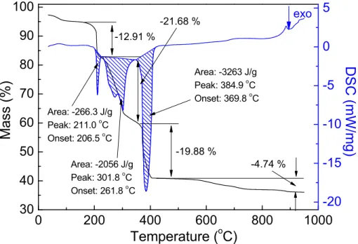
To remove the organic compounds and obtain the Bi-2212 phase, a thermal treatment is applied in a laboratory box furnace according to a differential scanning calorimetry (DSC)
and thermogravimetric analysis (TGA) as presented in Figure 1. The temperature of the
final step thermal treatment is over 800◦C as for the solid thermal synthesis of bulk materials,
the sample obtains the phase at 825 ◦C. An additional treatment at 500 ◦C in pure O2
environment is required to compensate the oxygen loss during the former heat treatment process. 0 200 400 600 800 1000 30 40 50 60 70 80 90 100 Area: -3263 J/g Peak: 384.9 o C Onset: 369.8 o C Area: -2056 J/g Peak: 301.8 o C Onset: 261.8 o C -4.74 % -19.88 % -21.68 % D S C ( m W / m g ) M a ss ( % ) Temperature ( o C) exo -12.91 % Area: -266.3 J/g Peak: 211.0 o C Onset: 206.5 o C -20 -15 -10 -5 0 5
FIG. 1. Result of the differential scanning calorimetry (DSC) and thermogravimetric analysis (TGA) about the as-prepared nanowires
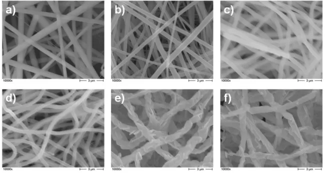
Figure 2 shows scanning electron microscopy (SEM) images of the nanowires at different steps of the thermal treatment, images (a) - (e) present the undoped nanowires (1112 sam-ple), and (f) the Pb-doped one. Before the thermal treatment, the as-prepared nanowires are tenacious and straight because the polyvinylpyrrodione helps to strengthen the inner connection of the wire. As the fibers experience higher temperature treatments, the organic compound is gradually removed and the wire structure starts to bend. Meanwhile, with the crystallization process the grains grow larger. It can be seen that after the thermal treatment, the nanowires are not as smooth as the as-prepared nanowires due to the growth of the crystal grains. The junction between the grains becomes the main connection way to maintain the wire structure, instead of binding by polymer. Figure 2 (e) and (f) present the
final structures of the 1112 sample and Pb-doped sample after the 800 ◦C treatment and
FIG. 2. SEM image of the undoped nanowires (a)-(e) and Pb-doped nanowires (f) at magnification (10000×) at different thermal treatment steps. (a) As-prepared, (b) 211 ◦C, (c) 302 ◦C, (d) 385
◦C, and images (e), (f) give the microstructures obtained after a treatment at 800 ◦C in air and
500◦C in O2 environment, respectively.
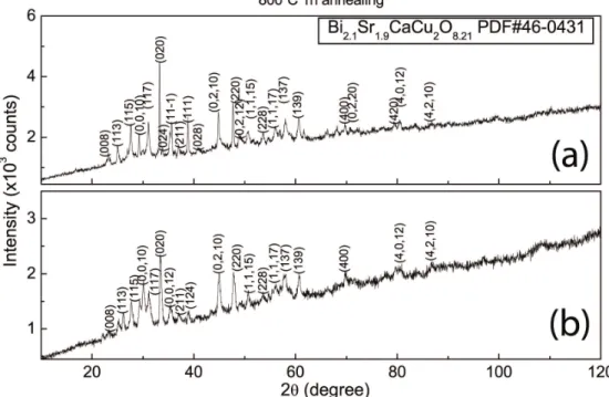
Figure 3 shows the X-ray diffraction results of the 1112 (a) and the Pb-doped samples (b) via a high-resolution automated RINT2200 X-ray powder diffractometer, using
Cu-Kα radiation generated at 40 kV and 40 mA. It turns out that with both precursors, the
nanowires can obtain the Bi-2212 phase after the thermal treatment. According to the analysis of the peaks, the average grain size of the 1112 sample is about 46.1 nm. However, the 5% Pb-doped sample presents a worse crystallinity than the 1112 sample, as the peaks from the spectrum have larger FWHM (full width at half maximum) values, and the average grain size is also found to be smaller, i.e., 39.1 nm. This can be attributed to the influence of the lead addition, as the Pb-doping faciliates the formation of the Bi-2212 phase, however, it also induces a lattice distortion.
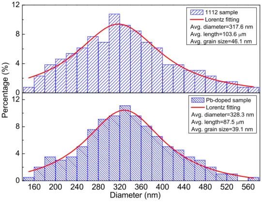
The nanowires obtained from electrospinning method always have a variation of the diameter. Figure 4 shows the distribution of the wire diameter from both samples. The value has a range from 140 to 580 nm. Table II shows the structure comparison of the 1112 sample and the Pb-doped sample. Generally, the two different types of samples share the similar structure, except that the grain size of the Pb-doped one is smaller. The average
FIG. 3. X-ray diffraction analysis of the nanowires samples after the whole thermal treatment, the phases have been identified as Bi2.1Sr1.9CaCu2O8.21 by the standard PDF card #46-0431. (a) the
1112 sample, and (b) the Pb-doped sample.
Parameters (averaged) 1112 Pb-doped Length (µm) 103.6 87.5 Diameter (nm) 317.6 328.3 Grain size (nm) 46.1 39.1
TABLE II. Structure comparison of the 1112 sample and the Pb-doped sample.
wire diameters of both samples are around 320 nm, which is in the range of the London
penetration depth18.
III. EXPERIMENTAL PROCEDURE
A. Magnetic measurement
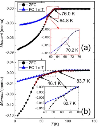
The superconductivity of both the 1112 and Pb-doped samples has been investigated for their magnetic behavior via the superconducting quantum interference device (SQUID). Figure 5 shows their magnetization dependence on temperature, in (a) the 1112 sample
160 200 240 280 320 360 400 440 480 520 560 0 4 8 12 0 4 8 12 Diameter (nm) P e r c e n t a g e ( % ) 1112 sample Lorentz fitting Avg. diameter=317.6 nm Avg. length=103.6 m Avg. grain size=46.1 nm
Pb-doped sample Lorentz fitting Avg. diameter=328.3 nm Avg. length=87.5 m Avg. grain size=39.1 nm
FIG. 4. The diameter statistics of nanoires from the 1112 and the Pb-doped samples. The diameter distributions from both samples have a wide range from 140 nm to 580 nm. The average diameter of the 1112 sample is about 317.6 nm and the Pb-doped one is 328.3 nm.
while (b) the Pb-doped sample. As a comparison, the measurements are done in zero field cooling (ZFC) and 1 mT field cooling (FC) modes, during the measurement a detecting field 1 mT is applied. There are two onsets in the M (T ) curves. The first one can be
defined as the critical temperature (Tc) at which the samples change from normal state to
superconducting state, as the samples become diamagnetic below this temperature. The second onset is the one related to the magnetic irreversibility where the magnetic behavior
becomes irreversible below such a temperature19. For the 1112 sample, the T
c is obtained
around 76 K while for the Pb-doped sample Tc is located around 84 K, which is close to the
value of the bulk materials at 85 K. According to the result of the FC curves, they start to deviate the ZFC curve at around 70.2 K and 62.7 K in the 1112 sample and the Pb doped sample respectively, thus it can be estimated that the samples show the field irreversiblity at certain temperatures. For the nanowires with their diameter being comparable to the
penetration depth, the relatively lower Tcfrom the 1112 sample can be attributed to thermal
hand, with the Pb-doping, the sample shows a higher Tc. The influence of Pb-doping on the
superconducting properties of Bi-2212 has been investigated for a decade in bulk and thin film materials. It is well known that the additional Pb serves as a substitution of the bismuth in the lattice structure. Thus, it can increase the volume fraction of the superconducting
phase22 and reduce the electronic anisotropy of Bi-221223. A certain amount of Pb-doping
could introduce an enhancement of the superconductivity. However, with increasing doping level, the lattice distortion due to the Pb substitution will also produce a suppression of the
superconductivity24. -0.09 -0.06 -0.03 0.00 0 50 100 150 -0.16 -0.12 -0.08 -0.04 0.00 0.04 60 64 68 72 76 -0.015 -0.010 -0.005 0.000 64.8 K ZFC FC 1 mT M o m e n t ( m e m u ) 76.0 K (a) (b) M o m e n t ( m e m u ) T (K) 46.1 K 83.7 K ZFC FC 1 mT 40 50 60 70 80 -0.018 -0.012 -0.006 0.000 0.006 62.7 K 70.2 K
FIG. 5. Magnetization dependence on temperature of the nanowires. The onsets at each curve can be related to the Tc and the irreversibility temperature of the sample. (a) shows the 1112 sample
and (b) the Pb-doped sample.
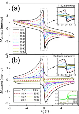
Figure 6 gives a comparison of the magnetization loops of the 1112 sample (a) and Pb-doped sample (b) in fields up to ±7 T in the temperature range from 5 K to 70 K. Starting
from 5 K, all the loops get fully asymmetric. The so-called fishtail effect25 in the
magne-tization loops can be seen in form of a minimum of the magnetic moment close to the full penetration field [see the upper inset to 5 (b)], and double sharp peaks occur close to zero field. Furthermore, the magnetization loops are asymmetric at the axis M = 0. Compared
-8 -4 0 4 8 -2 -1 0 1 2 - 8 - 4 0 4 8 - 0.14 - 0.07 0.00 0.07 0.14 -6 -3 0 3 6 M o m e n t ( m e m u ) Pb doped nanowires 5 K 25 K 10 K 30 K 15 K 50 K 20 K 70 K H a (T) (b) 65 K 70 K (a) M o m e n t ( m e m u ) 5 K 10 K 15 K 20 K 25 K 30 K 50 K 70 K 1112 nanowires -1.6-0.8 0.0 0.8 1.6 -6 -3 0 3 6 -1.6-0.8 0.0 0.8 1.6 -2 -1 0 1 2
FIG. 6. The comparison of the M (H) loops of the samples ranging from 5 K to 70 K. (a) gives the data of the 1112 sample, and the inset presents the low-field part in detail. (b) shows the M (H of the Pb-doped sample. The upper inset presents details for low fields, and the lower inset shows the magnetization loops at 65 K and 70 K in detail.
to the typical symmetric loop of bulk cuprate superconductors26, the loops from both
sam-ples show a completely different behavior which reveals the polycrystalline character of the granular nanowires. In the case of the 1112 sample, the irreversible superconducting loop
maintains up to 70 K, corresponding to the result obtained from the M (T ) curve where Tc
is about 76 K. The diamagnetic background superposed on the loops can be attributed to the excess of Cu from the preparation, which forms the CuO impurity.
In the case of the Pb-doped sample, the irreversible superconducting loop vanishes above 65 K, and a reversible paramagnetic curve is observed. This demonstrates that above this temperature the irreversibility due to the flux pinning is gone, and no vortices are pinned in the sample. Such result has a good agreement with the irreversibiity starts at around 63 K from the M (T ) curve. We can conclude here that the pinning landscape of the Pb-doped sample is worse as compared to the 1112 sample, especially at high temperatures.
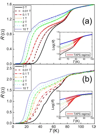
0 20 40 60 80 100 120 0.0 0.5 1.0 1.5 2.0 2.5 T (K) L o g ( R ) 0 T 0.01 T 0.1 T 1 T 2 T 6 T 10 T R ( ) T (K) (b) 60 70 80 90 100 0.3 0.6 0.9 TAPS regi m e 0.0 0.4 0.8 1.2 1.6 T (K) L o g ( R ) 0 T 0.01 T 0.1 T 1 T 2 T 6 T 10 T R ( ) (a) 60 70 80 90 100 1.0 1.2 1.4 1.6 TAPS regi m e
FIG. 7. Comparison of the resistance-temperature behavior of the samples as a function of tem-perature ranging from 4 K to 120 K, with an applied current of 50 µA. (a) gives the data of the 1112 sample and (b) the data of the Pb-doped sample.
B. Electric properites
In order to clarify whether the Pb-doping has a positive or negative influence to the superconductivity of the sample, four-probe measurement is applied to investigate the re-sistance dependence on temperature. Before the connection to the electrodes, the samples have been coated with 100 nm gold as to enhance the contact quality.
Figure 7 shows the results of both samples from 4 K to 120 K in the field range from 0 T to 10 T [(a) for 1112 sample and (b) for Pb-doped sample]. The two step behavior of the resistance drop occurs in both samples. The first drop of resistance stems from the sample phase transition from the normal state to the superconducting state. The values of
the normal state resistance RN28 can be estimated as 1.59 Ω at 115.7 K and 2.25 Ω at 87.5
K from the 0 T curves of the 1112 sample and the Pb doped sample respectively. However,
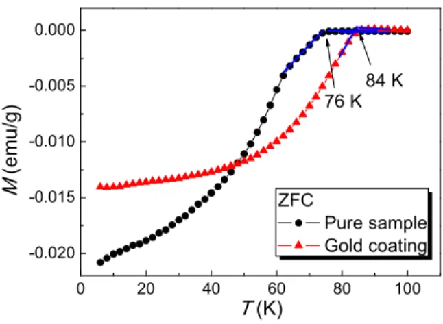
0 20 40 60 80 100 -0.020 -0.015 -0.010 -0.005 0.000 M ( e m u / g ) T (K) ZFC Pure sample Gold coating 84 K 76 K
FIG. 8. M (T ) measurements before and after the gold coating
the samples is not available. The non-zero resistance broadening of the curves around Tc
shows an exponential relationship with the inverse of the temperature. Such regimes can be fitted by the mathematic expression exp(−∆F/kT ) (see the insets to Fig. 7). ∆F is the energy required to locally suppress superconductivity. This indicates that the resistances
are resulting from the thermal activated phase slip (TAPS)27. The residual resistance at
the second step is the one due to the intergrain weak links inside the nanowires29. With
increasing field, the regime of the first step becomes even broader due to the enhanced phase
slip rate with field30. Such effect is more sensitive than the variation of RN in field, thus the
two steps get closer at higher field. At 10 T applied field, the steps merge to one.
In the case of the 1112 sample, the onset of superconductivity is about 85 K, which means that the value of critical temperature is higher than the one from the M (T ) curve, 76 K. The 9 K enhancement can be attributed to the influence of the coating gold layer, which has been proven by the comparison of the M (T ) curves with and without gold coating (Figure
??). To the Pb-doped sample, the 0 T curve shows a Tc around 78 K. Considering the same
thickness of gold layer which contributes a similar increase to the Tc, we can estimate that
the Tc of the Pb-doped sample is about 68 K, which is much lower than the one obtained
from the M (T ) curve.
The superconductivity increasement from the gold is opposite to the proximity effect
that metal layer decreases the Tc of the superconductor. One of the possible explanation is
that the gold layer introduces the intergrain Josephson coupling to the sample, leading to a
IV. CONCLUSION
The Bi-2212 nanowire networks have been fabricated by electrospinning method and the consequent thermal treatment. In order to obtain the superconducting phase, the excess of copper, calcium salts and the Pb-doping (as the substitution of bismuth) are applied as two treatments to the precursors. The samples from both precursors show a similar polycrystalline nanowire structure with the wire diameter comparable to the penetration depth. According to the XRD result, the 1112 sample is better crystallized than the Pb-doped sample. The magnetic measurements reveal clear differences between the two samples.
From the M (T ) measurement, the Pb-doped sample has a higher value of Tc than the 1112
sample, however, the M (H) measurement shows the opposite. In the R(T) measurement, a two-step drop of the resistance is observed in both samples. The nonzero resistance from these two steps can be explained by the influence of TAPS and intergrain weak links inside the nanowires. The gold coating on the sample surface successfully solves the Schottky contact problem between the sample and the electrodes, giving a positive influence to the
superconductivity. The Tc results from the R(T) show a good agreement with the ones
obtained from the M (H) measurements. As a conclusion of the present measurements, both excess of Cu-, Ca- and Pb-doping can help to form the Bi-2212 phase. The sample
synthesized from the former method presents a better crystallinity, relative higher Tc than
the latter one. It indicates that to the electrospinnng polycrystalline nanowire, the influence of lattice distortion from Pb-doping is dominant.
ACKNOWLEDGMENTS
We thank Prof. V. Presser (INM Saarbr¨ucken and Saarland University) for the possibility
to use the electrospinning apparatus and Dr. J. S. Atchinson (INM Saarbr¨ucken) and J.
Schmauch (Saarland University, group Prof. Birringer) for technical assistance. This work is supported by Volkswagen Foundation. The collaboration UdS-Nancy was supported by an EU-INTERREG IVa project ”Greater Region Magnetism Network (GRMN)”.
REFERENCES
1A. Bezryadin, C. N. Lau, and M. Tinkham, ”Quantum suppression of superconductivity
in ultrathin nanowires”, Nature 404, 971 (2000).
2S. H. Lai, Y. C. Hsu, and M. D. Lan, ”Synthesis of Bi
2Sr2CaCu2Oy nanowire and its
superconductivity”, Solid State Commun. 148, 452 (2008).
3L. Zhang, L. You, D. Liu, W. Zhang, L. Zhang, X. Liu, J. Wu, Y. He, C. Lv, Z. Wang,
and X. Xie, ”Characterization of superconducting nanowire single-photon detector with artificial constrictions”, AIP Advances 4, 067114 (2014).
4A. Korneev, P. Kouminov, V. Matvienko, G. Chulkova, K. Smirnov, B. Voronov, G. N.
Goltsman, M. Currie, W. Lo, K. Wilsher, J. Zhang, W. Slysz, A. Pearlman, A. Verevkin, and R. Sobolewski, ”Sensitivity and gigahertz counting performance of NbN supercon-ducting single-photon detectors”, Appl. Phys. Lett. 84, 5338 (2004).
5C. N. Lau, N. Markovic, M. Bockrath, A. Bezryadin, and M. Tinkham, ”Quantum phase
slips in superconducting nanowires”, Phys. Rev. Lett. 87, 217003 (2001).
6D. S. Golubev, and A. D. Zaikin, ”Thermally activated phase slips in superconducting
nanowires”, Phys. Rev. Lett. 78, 1 (2008).
7D. S. Golubev, and A. D. Zaikin, ”Quantum tunneling of the order parameter in
super-conducting nanowires”, Phys. Rev. B 64, 014504 (2001).
8I. Sochnikov, A. Shaulov, Y. Yeshurun, G. Logvenov, and I. Boˇzovi´c, ”Large oscillations of
the magnetoresistance in nanopatterned high-temperature superconducting films”, Nature Nanotechnol. 5, 516 (2010).
9E. Bar, D. Levi, G. Koren, A. Shaulov, and Y. Yeshurun, ”Transport properties of
ultra-thin granular YBa2Cu3O7−δ nanobridges”, Physica C 506, 160 (2014).
10J. Fransaer, J. R. Roos, L. Delaey, O. Van Der Biest, O. Arkens, and J. P. Celis, ”Sol-gel
preparation of high-Tc Bi-Ca-Sr-Cu-O and Y-Ba-Ca-O superconductors”, J. Appl. Phys.
65, 3277 (1989)
11D. Li, J. T. McCann, Y. Xia, and M. Marquez, ”Electrospinning: a simple and versatile
technique for producing ceramic nanofibers and nanotubes”, J. Am. Ceram. Soc. 89, 1861 (2006).
12J. I. Gorina, G. A. Kaljujnaia, V. I. Ktitorov, V. P. Martovitsky, V. V. Rodin, V. A.
of homogeneous BiSrCaCuO (2212) single crystals prepared by solution growth”, Solid State Commun. 85, 695 (1993).
13I. Chong, Z. Hiroi, M. Izumi, J. Shimoyama, Y. Nakayama, K. Kishio, T. Terashima,
Y. Bando, and M. Takano, ”High critical-current density in the heavily Pb-doped
Bi2Sr2CaCu2O8+δ superconductor: Generation of efficient pinning centers”, Science 276,
770 (1997).
14J. Shimoyama, Y. Nakayama, K. Kitazawa, K. Kishio, Z. Hiroi, I. Chong, and M. Takano,
”Strong flux pinning up to liquid nitrogen temperature discovered in heavily Pb-doped and oxygen controlled Bi2212 single crystals”, Physica C 281, 69 (1997).
15J. S. Atchinson, M. Zeiger, A. Tolosa, L. M. Funke, N. J¨ackel, and V. Presser,
”Electro-spinning of ultrafine metal oxide/carbon and metal carbide/carbon nanocomposite fibers”, RSC Adv. 5, 35683 (2005).
16J. M. Li, X. L. Zeng, A. D. Mo, and Z. A. Xu, ”Fabrication of cuprate
superconduct-ing La1.85Sr0.15CuO4 nanofibers by electrospinning and subsequent calcination in oxygen”,
CrystEngComm. 13, 6964 (2011).
17X. L. Zeng, M. R. Koblischka, and U. Hartmann, ”Synthesis and characterization of
elec-trospun superconducting (La,Sr)CuO4 nanowires and nanoribbons”, Mat. Res. Express 2,
095022 (2015).
18R. Prozorov, R. W. Giannetta, A. Carrington, P. Fournier, R. L. Greene, P. Guptasarma,
D. G. Hinks, and A. R. Banks, ”Measurements of the absolute value of the penetration
depth in high-Tc superconductors using a low-Tc superconductive coating”, Appl. Phys.
Lett. 77, 4202 (2000).
19M. R. Koblischka, X. L. Zeng, T. Karwoth, T. Hauet, and U. Hartmann, ”Magnetic
properties of electrospun non-woven superconducting fabrics”, AIP Advances 6, 035115 (2016).
20T. Aref, A. Levchenko, V. Vakaryuk, and A. Bezryadin, ”Quantitative analysis of
quan-tum phase slips in superconducting Mo76Ge24 nanowires revealed by switching-current
statistics”, Phys. Rev. B 86, 024507 (2012).
21M. Tinkham, C. N. Lau, and N. Markovic, ”Resistance induced by quantum phase-slips
in superconducting nanowires”, Physica E 18, 308 (2003).
22N. Hudakova, V. Plechacek, P. Dordor, K. Flachbart, K. Knizek, J. Kovac, and M.
BSCCO superconductors”, Supercond. Sci. Technol. 8, 324 (1995).
23L. Winkeler, S. Sadewasser, B. Beschoten, H. Frank, F. Nouvertn´e, and G. G¨untherodt,
”Interlayer coupling in Pb-substituted Bi2Sr2CaCu2O8 single crystals”, Physica C 265,
194 (1996).
24A. Sotelo, Sh. Rasekha, G. Constantinescu, H. Amaveda, M. A. Torres, M. A. Madre,
and J. C. Diez, ”Effect of Pb doping on the electrical properties of textured Bi-2212 superconductors”, J. Eur. Ceram. Soc. 34, 2977 (2014).
25M. Werner, F. M. Sauerzopf, H. W. Weber, and A. Wisniewski, ”Fishtail effect in the
magnetization of superconducting RBa2Cu3O7−δ (R=Y, Nd, Yb) and Y2Ba4Cu8O16single
crystals”, Phys. Rev. B 61, 14795 (2000).
26O. Kizilaslan, G. Kirat, and M.A. Aksan, ”Magnetic relaxation behavior in the
Bi2Sr2Ca2Cu3−xMoxO10+δ system fabricated by glass-ceramic technique”, J. Magn. Magn.
Mater. 384, 186 (2015).
27K. Xu, and J. R. Heath, ”Long, highly-ordered high-temperature superconductor nanowire
arrays”, Nano Lett. 8, 3845 (2008).
28H. M. Jaeger, D. B. Haviland, B. G. Orr, and A. M. Goldman, ”Onset of superconductivity
in ultrathin granular metal films”, Phys. Rev. B 40, 182 (1996).
29A. T. Bollinger, A. Rogachev M. Remeika, and A. Bezryadin, ”Effect of morphology on the
superconductor-insulator transition in 1-dimensional nanowires” Phys. Rev. B 69, 180503 (2004).
30M. Tinkham, ”Resistive transition of high-temperature superconductors”, Phys. Rev. Lett.
61, 1658 (1988).
31O. Yuli, I. Asulin, O. Millo, and D. Orgad, ”Enhancement of the superconducting transition
temperature of La2−xSrxCuO4 bilayers: Role of pairing and phase stiffness”, Phys. Rev.