HAL Id: hal-02999759
https://hal.archives-ouvertes.fr/hal-02999759
Submitted on 29 Dec 2020HAL is a multi-disciplinary open access archive for the deposit and dissemination of sci-entific research documents, whether they are pub-lished or not. The documents may come from teaching and research institutions in France or abroad, or from public or private research centers.
L’archive ouverte pluridisciplinaire HAL, est destinée au dépôt et à la diffusion de documents scientifiques de niveau recherche, publiés ou non, émanant des établissements d’enseignement et de recherche français ou étrangers, des laboratoires publics ou privés.
Progress and prospects for ultrathin solar cells
Inès Massiot, Andrea Cattoni, Stéphane Collin
To cite this version:
Inès Massiot, Andrea Cattoni, Stéphane Collin. Progress and prospects for ultrathin solar cells. Nature Energy, Nature Publishing Group, 2020, 5, pp.959-972. �10.1038/s41560-020-00714-4�. �hal-02999759�
Progress and prospects for ultrathin solar cells
Inès Massiot
(a), Andrea Cattoni
(b,c)and Stéphane Collin
(b,c)*(a) Laboratoire d'Analyse et d'Architecture des Systèmes (LAAS-CNRS), Université Toulouse, CNRS, Université Paul Sabatier, 31031 Toulouse, France
(b) Centre de Nanosciences et de Nanotechnologies (C2N), CNRS UMR 9001, Université Paris-Saclay, 91120 Palaiseau, France
(c) Institut Photovoltaïque d'Ile-de-France (IPVF), CNRS UMR 9006, 91120 Palaiseau, France *email : [email protected]
Abstract
Ultrathin solar cells with thicknesses at least 10 times lower than conventional solar cells could offer a unique potential to efficiently convert solar energy into electricity while enabling material savings, shorter deposition times, and improved carrier collection in defective absorber materials. Efficient light absorption and hence high power conversion efficiency could be retained in ultrathin absorbers using light-trapping structures that enhance the optical path. Nevertheless, several technical challenges prevent the realization of a practical device. Here we review the state-of-the-art of c-Si, GaAs and Cu(In,Ga)(S,Se)2 ultrathin solar cells and compare their optical performances against
theoretical light-trapping models. We then address challenges in the fabrication of ultrathin absorber layers and in nanoscale patterning of light-trapping structures and discuss strategies to ensure efficient charge collection. Finally, we provide perspectives to combine photonic and electrical constraints into practical architectures for ultrathin solar cells and identify future research directions and potential applications of ultrathin photovoltaic technologies.
Introduction
The share of photovoltaics in renewable energy production is expected to grow from 6.6% in 2017 to 18.9% in 20301. Reaching this target requires not only increases in solar cell efficiencies but also reduction in their cost. The efficiency of single-junction solar cells based on monocrystalline semiconductors is now close to the theoretical Shockley-Queisser (SQ) limit. With respect to a SQ limit of 33.5%2, GaAs solar cells achieved a 29.1% efficiency with a 1-2 µm thick absorber layer3,4. The indirect bandgap of crystalline silicon (c-Si) is responsible for Auger recombination and much weaker light absorption which results in a lower theoretical efficiency limit of 29.4%5 and a record of 26.7% for 165 µm-thick silicon solar cells6. The efficiency of polycrystalline solar cells, instead, is still far from the theoretical SQ limit due to lower material quality. Efficiencies of about 23% have been
demonstrated for CdTe and Cu(In,Ga)(S,Se)2 (CIGS) semiconductors with 2-4 µm-thick absorber
layers4,7.
In all these solar cells, relatively thick absorbers have been used to ensure that most incident photons are absorbed in a single pass through the cell. However, the effective optical path length can be increased several times by trapping light in the absorber, so that the same values of photogenerated currents and efficiencies can be preserved in much thinner solar cells8. With efficient light-trapping strategies, the thickness of solar cells could be reduced by more than one order of magnitude. We refer to ultrathin solar cells as a 10-fold decrease in absorber thickness with respect to conventional solar cells, corresponding to thicknesses below 20 µm for c-Si and 400 nm for thin films as GaAs, CdTe and CIGS.
Numerous benefits are expected from thinner cells. Reducing the material consumption is a direct source of cost reduction in the case of scarce elements (e.g. tellurium in CdTe, indium in CIGS and III-V semiconductors). The decrease of deposition times associated with thinner layers directly translates into an increase of the industrial production throughput and lower capital investment costs. From a device perspective, in the case of ultrathin solar cells limited by radiative (GaAs), Auger (Si) or other bulk recombinations (CIGS, CdTe), the open-circuit voltage increases with reduced absorber thickness8,9,10. The carrier collection is also improved in high defect density materials with limited diffusion lengths (CIGS, CdTe). For silicon solar cells, thinning silicon wafers from 160 µm to 50 µm could reduce both manufacturing cost and capex11. Beyond, efficiency limits above 28.5% are predicted for thicknesses as low as 10 μm8,12. With such thin silicon thicknesses, low-cost chemical vapor deposition (CVD) becomes an appealing deposition technique combining high throughput and low material consumption13.
Many light-trapping structures were first implemented in amorphous or micro-crystalline silicon solar cells14 and contributed to the development of concepts that are now applied to more efficient devices. Likewise, the simple fabrication processes of emerging technologies such as perovskites, organic photovoltaics or colloidal quantum dot solar cells, facilitate the implementation of light-trapping strategies like plasmonics15 or photonic crystals16. However, most efforts in these fields have been dedicated to material and stability issues rather than advanced light-trapping and thickness reduction17.
So far, most research on ultrathin solar cells has been focused on developing advanced light-trapping strategies based on patterning techniques at the nanometer scale. Assuming Lambertian light-trapping, state-of-the-art efficiencies (c-Si: η>26%, GaAs: η>29%, CIGS: η>23%) could be reached for 10 µm-thick c-Si solar cells and 100 nm-thick GaAs or CIGS thin films. However, downscaling the absorber layer thickness challenges the whole design of solar cell architectures. For instance, a longer optical path could increase parasitic absorption in contact layers that do not contribute to photogenerated carriers collected in the device. Texturation of the absorber may also increase
non-radiative surface recombination. Overall, the issues of carrier photogeneration and collection are deeply interconnected and thinning the absorber further constrains the realization of selective contacts and passivation layers. Fulfilling the potential of ultrathin solar cells thus requires a comprehensive understanding of the issues limiting the performances of current works.
Here we provide a critical overview of recent advances in ultrathin solar cells based on industrially mature technologies (c-Si, GaAs, CIGS). We discuss generic approaches that can be applied to emerging technologies or to thin-films made of CdTe18 or kesterites19, for which a thickness reduction has been less explored. In order to highlight the potential in thickness reduction, we first review the progress made in trapping light in ultrathin layers, including numerical works and experimental demonstrations and we analyze the gap between current optical performances and reference models. We then discuss advances and challenges in the fabrication of ultrathin absorber layers and nanoscale texturation for light-trapping. Subsequently, we focus on the most promising strategies to ensure efficient charge carrier collection in ultrathin devices, tackling key issues of surface passivation and carrier selectivity. Finally, we present envisioned architectures for ultrathin solar cells, integrating both aspects of light absorption and charge carrier collection, and we draw perspectives on future directions for research and applications of ultrathin solar cell technologies.
Benchmarking optical performance of ultrathin solar cells
Light absorption is strongly wavelength-dependent and drops with decreasing absorber thickness. For example, less than 40% of photons are absorbed in a single pass above λ=650 nm for a 2 µm-thick c-Si solar cell. Enhancing light absorption in the long wavelength range (close to the bandgap) is thus critical to ensure good conversion efficiency in ultrathin solar cells.
Box 1 introduces the concept of light-trapping and presents three reference models which we use to analyse the performances of ultrathin c-Si, GaAs and CIGS solar cells: single-pass absorption, double-pass absorption, and Lambertian scattering. In order to compare light-trapping efficiencies, we plot the short-circuit current density Jsc as a function of the absorber thickness. Jsc is the measure of the
number of photogenerated carriers collected in the device under sunlight illumination. Assuming a perfect collection of photogenerated carriers, the absorption efficiency is equal to the external quantum efficiency (EQE) and the short-circuit current is given by = × . ,
where q is the electronic charge and . is the spectral photon flux of the AM1.5G solar
spectrum. The thickness considered in the benchmark of ultrathin solar cells is that of the absorber. Window, buffer and back surface field layers, as wide bandgap semiconductors in heterojunctions, are not taken into account. In the case of structured absorbers (textured surfaces, nanowires, etc.), we use the equivalent thickness of a planar absorber with the same volume.
We restrict this literature review to single-junction solar cells measured under the calibrated AM1.5 global solar. Since most studies of ultrathin solar cells are still in their infancy, this benchmark is not restricted to solar cells independently measured by a recognized test center. We report only on solar cells with an area ≥ 1mm2, with the exceptions of ultrathin GaAs solar cells with surface areas down to
300x300 µm2. The complete data set used in the analysis is provided in the Supplementary Dataset file.
BOX 1: Light-trapping in solar cells
Absorption in a semiconductor layer is primarily determined by its intrinsic material properties (complex refractive index + ) and thickness . The absorption coefficient = 4 ⁄ is strongly material- and wavelength-dependent. Panel (a) illustrates the difference in behavior of direct (GaAs, CIGS) and indirect (c-Si) bandgap semiconductors, and the steep decrease of close to the bandgap. The refractive indices are provided in the Supplementary Dataset file for GaAs and CIGS, and taken from literature for crystalline silicon185. Additional coatings, back mirror and texturation can affect the way light enters the cell, propagates, scatters, is trapped and resonates in the absorber, and counter-balance the low absorption in a given wavelength range. The optical path enhancement factor F can be used as a figure-of-merit for the efficiency of light-trapping within a solar cell. Absorption at each wavelength is then expressed as = 1 − .
In the following, we consider three light-trapping models as references to analyze the performances of ultrathin solar cells. The corresponding reference absorption spectra are plotted for a 2 µm-thick slab of c-Si in panel (b). For single-pass absorption (panel (c)), we assume a perfect anti-reflection coating (ARC) with no backside reflection: = 1. Adding a perfect back reflector leads to double-pass absorption (panel (d)), and = 2. Light scattering on a sub-wavelength texture (panel (e)) is the most common way to increase the optical path length in the absorber. It is accomplished through random texturation of the surface or via nanoparticle ensembles. The maximum optical path enhancement factor F requires Lambertian scatterers with perfect ARC and a back mirror186. Under these conditions, full randomization of light ray directions and internal reflections result in the Lambertian scattering model, which is described more accurately by = ⁄ and = 4 187. For inorganic semiconductors, ≈ 50. The remarkable absorption enhancement that can be achieved theoretically with Lambertian light-trapping compared to single-pass and double-pass absorption is highlighted in panel (b). Periodic patterning has also been investigated as an alternative for light absorption enhancement (panel f). Recent theoretical works suggest that multi-resonant absorption can exceed the absorption enhancement enabled by Lambertian scattering188,189 but no general model setting the theoretical upper limit for light-trapping is available yet.
These light-trapping strategies require texturation or nanostructures at the vicinity of the absorber. Alternatively, external texturation using micro-textured foils190 or imprint-textured glass superstrates191 can contribute to light management in planar or textured absorbers. In both cases, they result not only in enhanced absorption but also in photon recycling effects induced by light-trapping9 or angular selectivity192,193. The concepts of external texturation and angular restriction have not been applied to ultrathin solar cells yet.
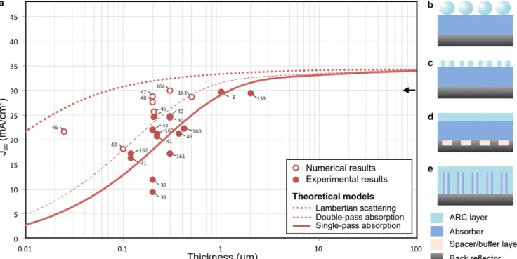
Ultrathin c-Si solar cells.Most of the experimental Jsc values for state-of-the-art c-Si solar cells lie
close to the single-pass absorption reference curve (Figure 1). Interestingly, the different fabrication processes are clustered in specific thickness ranges. Solar cells thicker than 10 µm are typically fabricated by liquid phase epitaxy (LPE), CVD, or exfoliated from a silicon wafer. For these absorber thicknesses, the light-trapping strategies are limited to the combination of an ARC and a front texturation made of micrometer-scale random pyramids, as conventionally used for wafer-based silicon cells. Best short-circuit currents reach Jsc=37.9 mA/cm² for 47 µm-thick solar cells13,20,13. As the c-Si thickness decreases, there is a clear increase in the complexity of the strategies used to enhance light absorption. Solar cells thinner than 10 microns require specific fabrication techniques for the absorber layer (epitaxial growth, recrystallization, layer transfer) and sub-micrometer texturation with novel geometries.
Figure 1. State-of-the-art of ultrathin monocrystalline Si solar cells. (a) Short-circuit current density (Jsc) of thin
(20 µm ≤ t ≤ 100 µm) and ultra-thin (< 20 µm) monocrystalline silicon (c-Si) solar cells as a function of the absorber thickness10,12,13, 20-24,26-32,34-36,75,80-83,87,121-158. Experimental results are indicated with filled colored triangles and grouped according to the crystal growth method (from Si wafers, epitaxy or recrystallization). The use of a layer transfer process is shown with a black dot overlaid with the coloured triangles. Jsc values from numerical calculations and absorption measurements are indicated with open triangles. All reported values are compared to the reference models defined in Box 1 (curves). The Jsc value of the record-efficiency
c-Si solar cell is indicated by an arrow6. (b-g) Sketches of notable light-trapping schemes used in state-of-the-art thin and ultrathin c-Si cells: (b) micron-scale random pyramids10,12213,20,121-126, (c) front inverted nanopyramid arrays21,22, (d) amorphous ordered nanopatterning23, (e) slanted cones29, (f) front and back nanocone arrays27 and (g) photonic crystals31
In the sub-10 µm range, three noticeable experimental works have demonstrated a short-circuit current density exceeding double-pass absorption21,22,23. Their common light-trapping strategy is based on the use of a sub-micrometer front texturing of silicon coupled with a metal back reflector. A short-circuit current of 34.5 mA/cm² has been achieved with 10 µm-thick silicon solar cells21. The light-trapping scheme integrates a 2D periodic array of inverted pyramids coated with a silicon nitride layer on the front side and an aluminium back mirror. This proof-of-concept device was fabricated using relatively expensive silicon-on-insulator (SOI) wafers and resulted in high conversion efficiency (η=15.4%).
The same light-trapping strategy with a silver back mirror implemented in a 3 µm-thick Si solar cell led to a short-circuit current density of 25.3 mA/cm² (equivalent thickness of c-Si of 2.75 µm) but an efficiency of only 5% limited by parasitic absorption and surface recombination22. In this case though, the c-Si layer was epitaxially grown by low temperature plasma-enhanced CVD (PECVD) and transferred on a glass substrate via anodic bonding and mechanical cleavage. The front texturing was fabricated using nanoimprint lithography (NIL) and wet etching.
Further thickness reduction led to a certified conversion efficiency of 8.6% (19.7 mA/cm2) for a 1.1 µm-thick c-Si layer produced by the “Epifree” method23. As an alternative to periodical pyramid
arrays, the front surface of the cell is textured with a short-range ordered arrangement of parabolic holes fabricated by colloidal lithography and dry etching. The significant conversion efficiency obtained for such a thin absorber layer (equivalent thickness of 830 nm) demonstrates that a submicron texturing of the absorber by dry etching can be combined with efficient passivation.
The last two approaches combine a bottom-up growth method (PECVD, epifree) with a layer-transfer process for an effective reduction of material usage and implement upscalable patterning techniques such as nanoimprint and colloidal lithography22,23. Industrially viable ultrathin silicon solar cells could stem from combining the best of these three works, applying bottom-up growth methods and scalable patterning techniques to the processing of 10 µm-thick silicon cells to reach efficiencies above 15%.
Figure 2. Light-trapping performances of notable ultrathin monocrystalline Si solar cells. EQE experimental data of patterned ultrathin c-Si solar cells with a nominal thickness t=10 µm21 (solid blue curve), 3 µm22 (solid red curve) and 1.1 µm23 (solid black curve). The EQE data for planar cells with the same thickness are shown as a reference (dashed lines). The colored regions represent the EQE enhancement induced by texturation.The thick plain lines show the fit of the EQE curves in the long wavelength region with the Lambertian model for the following values of F and the equivalent thickness: F=20 and deq=9.83 µm21, F=10 and deq=2.75 µm22 and F=7.5
and deq=0.830 µm23.
The light-trapping efficiency can be quantified by calculating the light path enhancement factor F with respect to single pass. In the weakly absorbing regime (α*d tends to zero), the absorption can be approximated by the Lambertian scattering model22 as expressed in Box 1. Hence F can be estimated for a particular light-trapping strategy by fitting EQE measurements with the Lambertian expression in a restricted wavelength range close to the bandgap. Note that the equivalent thickness of the textured silicon layer should be determined beforehand to be
implemented in the Lambertian model. Figure 2 illustrates the determination of light path enhancement factors for periodic 21,22 and disordered23 front texturations of the silicon layer. In the
case of F=10, the light path enhancement has been further decomposed into the combination of the increased effective thickness due to diffraction on the inverted pyramid array (x1.25 enhancement) and the reflection on both the front (x4) and back (x2) interfaces22.
Despite these promising advances, there is still a significant gap between light-trapping performances of experimental works and the Lambertian model (see Figure 1). Numerical studies using simplified cell designs explored novel geometries, from inverted pyramids12,24 to photonic crystals25, gratings26, nanocone arrays27, slanted cones28,29) and quasi-random structures (R58)30. Remarkably, the best numerical performances actually exceed the Lambertian reference using resonant modes in a slanted conical-pore photonic crystal combined with a back silver mirror28,29. Because of the simplified cell architecture, the predicted short-circuit currents are likely to be overestimated. Nevertheless, these works give us a hint of the potential gain using properly designed nanophotonic structures. The periodicity plays a key role in the design. Wavelength-scale front structuration can efficiently diffract light into the silicon absorber with negligible diffraction losses in air21,22 and asymmetry can increase the number of resonances as well as the overall absorption28,29. Models that include a complete solar cell structure lead to significantly lower performances31,32. Actually, most experimental works are still below the double-pass absorption. Aside from non-perfect antireflection coating, two main sources of losses should be taken into account in the cell design: losses in contact layers (parasitic absorption and non-radiative recombination) and absorption in the back mirror. Parasitic absorption occurs in transparent conductive oxides (TCO), the highly-doped contacts and the passivating layers and it is likely to be exacerbated by light-trapping31,32. Optical losses in the metal reflector are inevitable; in particular for nanostructured mirrors whenever surface plasmon resonances are excited. Losses can be reduced introducing a thin dielectric layer with a low refractive index between the silicon and the mirror33,34. This is normally accomplished in a PERC silicon cell by the Al2O3/SiN layer also used to define the localized contacts. Alternatively,
omnidirectional distributed Bragg reflector (DBR) with negligible losses can be designed to operate in the relatively narrow region of weak absorption of crystalline silicon. Almost 4n2 optical path enhancement has been demonstrated in 28 µm-thick Si using a front texturation coupled with an omnidirectional DBR reflector composed of only 6 pairs of a-Si/SiN layers35. When coupled with a back texturation, the DBR should be carefully designed to avoid transmission losses35,36.
Ultrathin GaAs solar cells. With a direct bandgap and a high radiative efficiency37, GaAs is a model system to explore novel light-trapping strategies that can be applied to other materials. Record single-junction solar cells with efficiency of 29.1% have been achieved with a back mirror that boosted both the Jsc (absorption improvement) and the Voc (photon recycling)3,4. In ultrathin solar cells, internal losses may still hinder photon recycling9 while light-trapping has been successfully used to improve Jsc. First attempts based on the use of metal nanoparticles as scatterers led to relatively low Jsc due to parasitic absorption and the lack of a back mirror38,39 (see Figure 3). These drawbacks were circumvented using gold deposited on a rough AlInP layer, acting as both a contact and a scattering
back mirror40 which resulted in Jsc=24.5 mA/cm2 (η=19.1%) for a 300 nm-thick GaAs layer40. Light-trapping and carrier collection can also be optimized separately by combining localized ohmic contacts and a high-reflectivity silver back mirror41. This idea was implemented using a rough back mirror fabricated by a simple wet chemical etching of an Al0.3Ga0.7Al contact layer and led to an
efficiency of 21.4% with Jsc=24.8 mA/cm242.
To further enhance light absorption, most recent approaches rely on periodic arrangements of nanostructures to excite resonant modes. They can be localized in dielectric nanostructures (Mie resonances)43 or preferably in the active layer by guided-mode resonances44,45. In the latter case, diffracted waves induced by the grating couple to waveguide modes. The spectral position and intensity of the resonance peaks can be tuned via the geometry of the nanostructures so that multiple resonances partially overlap leading to broadband absorption enhancement. Using this approach, dielectric nanostructure arrays deposited on the front surface of 200 nm-thick solar cells resulted in Jsc=22 mA/cm2 (η=16.2%)44. An improved Jsc of 24.6 mA/cm2 was obtained with a nanostructured back mirror fabricated by NIL and combined with localized contacts45. The latest result exceeds single-pass absorption by 7 mA/cm2, and has led to a certified efficiency of η=19.9%. A detailed loss analysis shows that the same architecture could lead to an efficiency of 25%.
Figure 3. State-of-the-art of ultrathin GaAs solar cells. (a) Short-circuit current density (Jsc) of thin (> 400 nm) and ultra-thin (< 400 nm) GaAs solar cells as a function of the absorber thickness3,38-46,48,49,159-164. Experimental results are indicated with filled circles. Jsc values from numerical calculations are indicated with open circles. All reported values are compared to the reference models defined in Box 1 (curves). The Jsc value of the best-efficiency GaAs solar cell is indicated by an arrow. (b-e) Sketches of notable advanced light-trapping schemes used in state-of-the-art ultrathin GaAs cells: (b,c) front dielectric nanostructure arrays43,44, (d) nanostructured back mirror45, and (e) nanowire arrays49.
The room left for absorption enhancement is explored by a few numerical studies. For very thin structures (25 nm), metal-semiconductor-metal plasmonic cavities exhibit broadband light absorption while keeping planar active layers46. Interestingly, another strategy relies on multi-resonant vertical nanostructures to induce a series of resonances regularly shifted spectrally47,48. A value of Jsc=28.8 mA/cm2 close to the Lambertian scattering model has been predicted with an array of nanocones corresponding to an equivalent thickness of 200 nm47. Though the structures proposed to date by these numerical studies are limited to simplified solar cell structures or exotic geometries difficult to fabricate, they can inspire the design of more realistic architectures that may reach or even overcome the performances predicted by the Lambertian scattering model. For now, nanowire-based solar cells are the closest practical example of a three-dimensional approach alternative to thin-film solar cells. They take advantage of a selective epitaxial growth and light-trapping properties intrinsic to the nanowire geometry and led to a record Jsc=21.4 mA/cm2 demonstrated with axial GaAs p-n junctions (equivalent thickness 370 nm, η=15.3%)49.
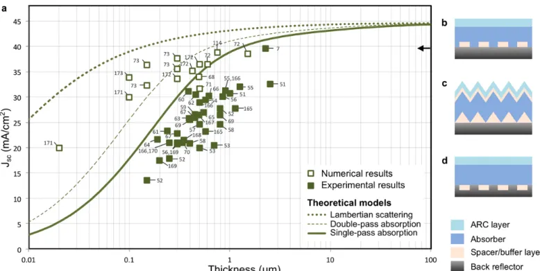
Ultrathin CIGS solar cells. Reducing the absorber thickness is a promising way to improve the
industrial competitiveness of CIGS photovoltaic modules, thanks to a lower material usage and an increased throughput50. The conventional structure of a CIGS solar cell is made of a CdS/Cu(In,Ga)Se2
heterojunction deposited on a molybdenum (Mo) back contact. Front side collection of electrons is ensured through undoped and Al-doped ZnO window layers coupled with an ARC. Depending on the CIGS composition, its bandgap may slightly vary around 1.15-1.2 eV. CIGS absorbers thinner than 1 µm have led to many experimental and numerical results, as reported in Figure 4. Remarkably, all the experimental results lie below the single-pass absorption.
This loss in Jsc is mainly attributed to parasitic absorption and surface recombination. On the front side, parasitic absorption occurs in the CdS buffer layer at short wavelengths, independently from the absorber thickness. It can be avoided through the use of wider bandgap Zn(O,S)-based buffer layers7. On the back side, parasitic absorption in the Mo contact resulting from low reflection at the CIGS/Mo interface occurs at longer wavelengths and its impact increases dramatically for ultrathin CIGS layers51,52,53,54,55,56,57,58,59. Additionally, higher surface recombination is induced in thinner absorbers by carriers photogenerated closer to the back contact52. It can be circumvented using thin (Al2O3, MgF2) passivation layers with nano-sized point contacts between CIGS and Mo,
resulting in Jsc=31.1 mA/cm2 (η=13.5%) for 385 nm-thick CIGS absorbers60, and Jsc=23.3 mA/cm2 (η=11.8%) for 240 nm-thick CIGS61.
Figure 4. State-of-the-art of ultrathin CIGS solar cells. (a) Short-circuit current density (Jsc) of thin (> 400 nm) and ultra-thin (< 400 nm) CIGS solar cells as a function of the absorber thickness7,51-73,165-173. Experimental results are indicated with filled squares. Jsc values from numerical calculations are indicated with open squares. All reported values are compared to the reference models defined in Box 1 (curves). The Jsc value of the best-efficiency CIGS solar cell is indicated by an arrow. (b-d) Sketches of notable advanced light-trapping schemes used in state-of-the-art ultrathin CIGS cells: (b) back dielectric nanostructure arrays64, (c) deposition on textured substrates72 and (d) nanostructured back mirror73.
Nanostructured dielectric layers have also been proposed to combine point contacts with increased optical reflectance and scattering at the CIGS/Mo interface. SiO2 nanostructures made by
NIL or nanosphere lithography have been introduced in 500nm-thick CIGS solar cells59,6259,63. It is worth noting that these devices cannot be directly compared to others due to a lower CIGS bandgap (~1 eV). A Jsc of 21.6mA/cm2 (η=9%) was demonstrated with 190 nm-thick CIGS deposited on a nanostructured SiO2 layer fabricated by interference lithography64. Still, the light-trapping efficiency
of these devices is limited by the low reflectivity of the Mo back contact. The choice of alternatice materials (ZrN 65 ,TCO66,67,68) is constrained by the high temperature of the CIGS deposition process. For this reason, highly reflective metals like Au69 and Ag70 have only been introduced in a superstrate configuration.
The optical design of light-trapping nanostructures has been hampered by the lack of reliable data for the CIGS refractive index close to the bandgap and by the presence of a composition gradient. Consequently, quantitative comparison between experiments, reference models, and numerical results should be handled with caution. Nevertheless, optical modeling has contributed to the assessment of optical losses in actual devices62,63,64, 67,69,6771 and provides guidelines for future designs. The integration of 2D pyramids arrays with a silver back mirror in a 600 nm-thick CIGS solar cell could lead to Jsc= 36.4 mA/cm272. The same Jsc has been predicted for only 150 nm of CIGS with a
periodically nanostructured silver back mirror73. To meet these predictions and unlock the performance of ultrathin CIGS solar cells, the main technological challenge currently pursued by many groups is the development of a back contact able to sustain CIGS deposition temperatures of about 500°C, provide a high optical reflectivity, and form an ohmic contact with CIGS with low surface recombination.
Fabricating ultrathin absorber layers
Best designs for light-trapping consist in a highly reflective back mirror combined with nanostructured front/rear surfaces to couple and guide light in the ultrathin absorber. Making these devices implies to tackle two issues that we discuss in this section: the fabrication of the ultrathin semiconductor layer and its transfer onto a back reflector.
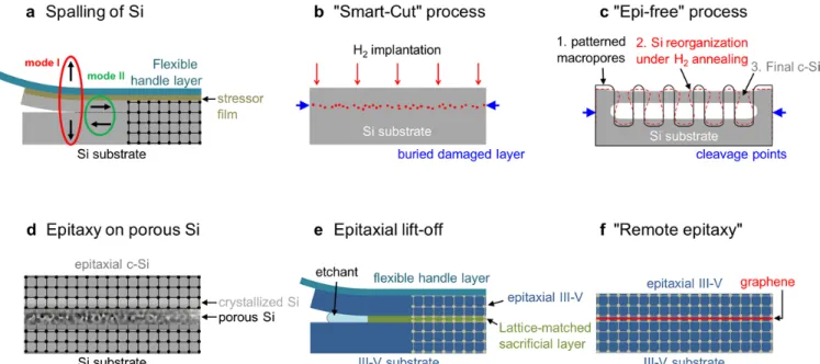
Ultrathin c-Si solar cells. The integration of a back mirror requires to transfer a thin film by exfoliation
from a thick wafer or by epitaxial growth and subsequent lift-off. The conventional process for producing silicon wafers out of the ingot uses a wire sawing technology. The material removed by the cutting blade (kerf) and wasted, about 40%, is likely to increase for ultrathin solar cells11.
The first logical evolution of this technology, named "kerfless wafering", is based on the mechanical exfoliation of a thin Si film from a thick wafer. The "spalling" process uses an applied stress to remove a film with a predetermined thickness in the range of a few tens of µm (Fig. 5a). The crack tends to follow a trajectory parallel to the film/substrate interface to minimize the shear stress component74. This technique has been used for 25 µm-thick c-Si solar cells with 14.9% efficiency75. It has also been used for Ge76 and III-V layers, and no degradation was observed in spalled GaAs solar cells with efficiency of 18.4% and Voc=1.07 V77. The simplicity of the technique makes it very attractive. However, the feasibility of multiple exfoliations from the same ingot over large surface areas and the precise control of the fracture depth layer thickness remain to be demonstrated.
The “smart-cut” process provides a way to precisely define the fracture interface at a determined depth from a few tens of nm up to about 10 µm by ion implantation78 (Fig. 5b)78. It has been implemented for SOI wafers destined to chip manufacturing and used for proof-of-concept photovoltaic devices as 10 µm-thick c-Si solar cells with 15.4% efficiency21. Yet, the viability of this process to fabricate solar cells in a cost-effective way at the industrial scale is questionable.
First introduced as silicon-on-nothing79, the “Epifree” process (Fig. 5c) is another technique for the mechanical exfoliation of thin Si films, still limited by the maximum thickness achievable (2-3 µm). Record ultrathin c-Si solar cells (8.6 %) have been successfully demonstrated using released 1 μm-thick high-quality monocrystalline thin films23.
Crystalline silicon thin films can also be fabricated by direct epitaxial growth techniques, such as LPE and CVD in various forms. CVD performed at relatively high temperatures offers high deposition rates (~µm/min) and has been widely used in a thickness range from 15 to 50 µm13,80,81. For thinner silicon films (1-10 μm), low-temperature PECVD and hot-wire CVD (HWCVD) have been developed recently and lead to high-quality layers with a lower thermal budget but also lower growth rates (50-300 nm/min)82,83. The introduction of a porous silicon layer prior to the epitaxial growth enables the release of an ultrathin silicon layer or even a complete solar cell (Fig. 5d). The residual porous Si is then removed and the substrate reused for additional growths84,85,86. This technique has led to remarkable Jsc values for different thicknesses13,22,80,81,87.
Ultrathin GaAs solar cells. Epitaxial growth is undoubtedly the most extensively used and versatile
approach for III-V semiconductors. The main challenge is to cost-effectively transfer the epitaxial layer on a host substrate. Using the "epitaxial lift-off" with an AlAs sacrificial layer88,89 (Fig. 5e), GaAs layers transferred onto a metallic mirror have led to record single-junction solar cells3. Cost reduction is still hindered by the limited number of substrate reuse (about a few tens).
Similarly to the epifree process, a germanium-on-nothing technology has also been developed to fabricate ultrathin single-crystal Ge membranes that can be used for epitaxial growth and transfer of GaAs solar cells90. 1mm2-area processed GaAs cells on a Ge membrane exhibit similar Voc values (0.835 V) as reference cells grown on bulk Ge.
Alternative methods to separate the epitaxial film from the substrate rely on the presence of a fragile interface or a poor adhesion between the template substrate and the epitaxial film. This idea was first implemented in the "CLEFT" process using a graphite mask patterned on a GaAs (110) substrate91. Nucleation and epitaxial growth start from the openings, continue by lateral overgrowth and produce a single-crystal GaAs film that can be mechanically cleaved. This technique has not been developed further despite promising 17%-efficient GaAs cells demonstrated in 198192.
More recently, a novel approach named "remote epitaxy" of thin films on (100) III-V semiconductor substrates covered with graphene has been proposed (Fig. 5f). Weak interactions allow lattice-matched epitaxy together with easier mechanical release93 and heteroepitaxy with a spontaneous relaxation of misfit strain94. The technique has been applied to transferred LEDS93, but not to photovoltaics yet. Large surface area and defect-free epitaxial growth still seems limited by the localized defects in the transferred graphene.
Ultrathin CIGS solar cells. The fabrication of polycrystalline CIGS ultrathin layers on back reflectors
raises specific challenges. CIGS is usually grown by co-evaporation, sputtering or electrodeposition on Mo, a refractory material that forms an ohmic contact with the CIGS thanks to the creation of a thin MoSe2 interface layer. Alternative back contact materials with higher optical reflectance and lower
surface recombination are currently under investigation in several groups66,67,70. Silver mirrors encapsulated with transparent conducting oxides appear as a promising candidate68.
Figure 5. Transfer techniques for monocrystalline semiconductor thin-films. (a) Spalling makes use of a stressor layer (metal or glue) deposited on the silicon wafer, that induces a pure opening stress (mode I) and a shear stress (mode II)74. (b) The “smart-cut” process is based on ion implantation to create a buried damaged layer at a specific depth78. Its expansion upon annealing (400-600°C) causes the detachment of the top thin silicon film with a relatively low roughness as compared to spalling. (c) In the “Epifree” process,cylindrical nanopore arrays are first etched in a silicon wafer that is subsequently recrystallized at high-temperature (1100°C) in inert atmosphere. Reorganization upon annealing results in a single-crystal silicon layer suspended on a void cavity23. (d) A fragile, recrystallized porous layer enables to detach and transfer the epitaxially grown silicon layers. (e) In the epitaxial lift-off of III-V, the peel-off of the absorber layer is accomplished by selectively etching a lattice-matched release layer sandwiched between the epitaxial layer and the substrate88,89. (f) In the remote epitaxy on graphene, the weak van der Waals potential of graphene cannot completely screen atomic interactions with the substrate allowing lattice-matched epitaxy together with easier mechanical release93.
Light-trapping nanostructures for ultrathin devices
A key challenge for ultrathin solar cells is to enhance light path in the cell to maintain a high absorption despite the thickness reduction. As discussed previously, sub-µm patterning is needed to scatter light or create multiple resonances in the absorber. Photolithography technologies using a projection lithography stepper21, interferences94, or Talbot effect96,97 are contactless techniques that meet the requirements for spatial resolution. However, their cost and long exposure time limit their use to proof-of-concept devices on small areas. In the framework of solar cell fabrication, specific techniques are required to structure matter at the nanoscale while being low-cost, scalable (patterned area >15x15 cm2) and versatile (in particular compatible to non-planar substrates). Figure 6 gathers nano-patterning techniques that we envision as promising for structuring ultrathin solar cells.
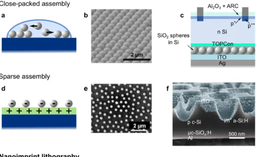
The use of the ordered (Fig. 6a-c) or disordered (Fig. 6d-f) self-assembly of colloidal particles (usually made of silica or polystyrene) is a simple patterning technique called nanosphere lithography. Close-packed arrangements are obtained by self-assembly of particles at air/water interface due to capillary forces (Fig. 6a-c). The colloidal crystal obtained can then be used as a mask or directly integrated in the solar cell as a diffractive structure (Fig. 6c)63,98. The scalability of close-packed colloidal assembly has been demonstrated over 1 m2 glass substrates99. An alternative technique, sparse assembly, relyies on electrostatic forces as particle-particle repulsion and particle-substrate attraction. It leads to an amorphous-ordered arrangement (Fig. 6e-f), which increases the number of accessible optical modes and can be of interest to achieve omnidirectional absorption. Sparse assembly has been used to texture the solar cell absorber100,101 or to integrate plasmonic antennas102. This technique combined with dry etching was employed to structure a 1.1 µm-thick c-Si layer with parabolic holes (Fig. 6f)23.
Nanoimprint lithography and its variants (Figs 6g-i) offer more flexibility in the design of patterns, from periodic arrays of squares103 or pyramids22 to disordered structures104,105. This replication technique is based on the embossing of a polymeric resist or a sol-gel derived metal-oxides material with a hard mold containing nanoscale surface-relief features106. To reduce costs, soft NIL uses a single expensive master mold replicated into many cheap polymeric stamps 107. Their flexibility allows low pressure embossing with a high tolerance to the substrate topography (Fig. 6g). It can be used as a conventional lithography technique with an additional step of pattern transfer. Using a Cr mask made by soft NIL, an array of inverted pyramid was etched in a 3 µm-thick silicon solar cell (Fig. 6h-i)22. Alternatively, the replicated nanostructures can be directly integrated without additional pattern transfer45,108, as demonstrated at the back contact of a III-V on Si triple junction solar cell using roll-to-plate nanoimprint of SU8 resist (Fig. 6k-l)103. It should be noted that current automated systems can pattern substrates as large as 0.5x0.5 m2 with resolution down to 20 nm and high throughput109.
Figure 6. Techniques to fabricate nanostructures and examples of integration in solar cells. (a-f) Nanosphere lithography: (a) schematics of air-water colloidal assembly; (b) SEM image of a close-packed assembly of 700 nm-large polystyrene nanospheres 99; (c) schematics of a silicon solar cell integrating silica nanospheres at the rear98; (d) schematics of sparse colloidal assembly relying on electrostatic interactions between charged colloids deposited on a oppositely charged substrate; (e) SEM image of the resulting amorphous colloidal distribution (sphere size: 270 nm)101; (f) SEM side view of an ultrathin (1.1 µm) silicon solar cell nanotextured using sparse colloidal assembly23. (g-l) Nanoimprint lithography: (g) schematics of the soft nanoimprint technique; (h,i) SEM top view and cross-section of an ultrathin silicon solar cell textured with inverted pyramids using a nanoimprinted etch mask22; (j) schematics of the roll-to-plate nanoimprint technique; (k) SEM image of a SU8 resist grating made by roll-to-plate nanoimprint and (l) schematics of a silicon solar cell integrating the nanoimprinted SU8 grating in the back contact103. Panels reproduced from: b, Ref. 99; e, Ref. 101; f, Ref. 23; k, Ref. 103. Panels adapted from: c, Ref. 98; h and i, Ref. 22; l, Ref. 103.
Collecting charge carriers
On both sides of the absorber, additional layers are needed to passivate the surfaces and collect charge carriers selectively toward the contacts. Under illumination, photogenerated carriers thermalize at the band edges and are described by two quasi-Fermi distributions. The collection of carriers should occur before recombination to ensure a high Jsc, and the quasi-Fermi level splitting should be maintained through the selective contacts to maximize the Voc.
Passivation. While defect-assisted (Shockley-Read-Hall) recombination decreases proportionally to
the absorber thickness t, the relative impact of surface recombination increases with the surface to volume ratio as 1/t. Recombinations at the surface are mediated by states with energies located in the forbidden bandgap, that originate from dangling bonds or defects at the interface between the absorber and a different material. Their density can be decreased by covering the absorber surface with dielectric layers (SiO2 or a-Si:H on c-Si, or sulfur-based compounds on III-V). Alternatively, their
impact can be reduced by "field effect" passivation using charged dielectric layers (Al2O3 on Si), or
composition gradients to repel minority carriers from the defective interface in CIGS. To combine passivation and collection of carriers, insulating passivation layers with local doping or metallic point contacts have been the most developed workaround in conventional crystalline silicon solar cells since the 90’s110 and more recently in CIGS60.
Selective contacts by doping. The separation of carriers occurs thanks to the different conductivities
of electrons and holes111, obtained by doping in homojunctions. However, ultrathin absorbers require relatively high doping: first, to keep the space charge layer confined in the junction thickness and ensure maximal VOC (>1018 cm-3 is required for 60 nm-thick GaAs) and, second, to preserve the
selectivity of the contacts under illumination (the conductivity of minority carriers increases with the density of photogenerated charge carriers as 1/t, assuming constant absorption). Heavy doping may induce many detrimental effects: increased long-wavelength parasitic absorption by free carriers, increased non-radiative recombination (defects, Auger), lower Voc due to bandgap narrowing (about
25 meV for 1018 cm-3). Furthermore, high doping levels are not yet achievable for some materials such as CIGS and CdTe.
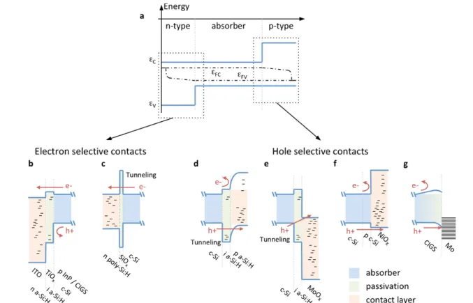
Heterocontacts. Heterostructures provide a way to overcome previous limitations and to design
full-area passivating selective contacts. Wide bandgap materials with the appropriate band offset (Fig. 7a) can act as selective contacts forming a high energetic barrier to prevent minority carrier recombination while enabling favorable band alignment and being highly conductive for majority carriers. Due to their wide band-gap and low density of minority carriers even under illumination, the constraints on doping are relaxed. In the case of III-V materials, suitable alloys can be grown lattice-matched on GaAs3. For other technologies (c-Si, polycrystalline thin films), heterocontacts are made of dissimilar materials with lattice-mismatched or crystalline/amorphous interfaces which are generally responsible for surface defects (Figure 7). A stack of disordered materials is commonly used for both surface passivation and carrier selectivity with suitable band offset or carrier tunneling mechanism.
These solutions are usually integrated in planar solar cells, but most of these approaches can be implemented on textured absorbers using conformal deposition methods, opening new possibilities to combine heterostructures and light-trapping in ultrathin solar cells designs. The solutions currently available should be further expanded by research on new materials and interfaces. For instance, wider bandgap semiconductors or TCO with appropriate band offset could help lowering parasitic absorption in the contact layers, in particular for hole collection.
Figure 7. Heterostructures for passivating selective contacts. (a) Band diagram of an ideal solar cell using n-type and p-n-type heterocontacts. The conduction and valence bands are indicated as εC and εV respectively
(solid blue lines). The electron and hole quasi-Fermi levels, εFC and εFV respectively, are indicated with
dash-dotted lines. (b-g) The dashed boxes point to examples of implementation of selective and passivating contacts for electrons (b,c) and holes (d-g). Schematic band diagrams are shown for illuminated solar cells at the maximum power point. The contacts are made of a first passivation layer (green), which decreases the density of surface defects or repels minority charges, and a second layer (orange) with appropriate band offsets, which creates a selective contact for majority carriers. Defect states in the gap are sketched with (-) marks. (b) Intrinsic and n-type a-Si:H layers for passivation and electron contact used in record c-Si solar cells6, and similar TiOx/ITO scheme174 on InP175 and CIGS176. (c) Tunnel oxide passivating contacts on Si177,178 implemented in 25.7
% efficiency with full-area contacts179. (d) intrinsic and p-type a-Si:H layers for passivation and hole contacts. (e) Hole contact made of large work function n-type MoOx, using hole tunneling through an intrinsic a-Si:H passivation layer on Si180,181,182. (f) NiOx p-type TCO used in combination with a p-type polycrystalline Si
layer150,Error! Reference source not found.. (g) CIGS/Mo contact showing a gradient of the indium to gallium ratio that leads to a shift of the conduction band maximum and contributes to the passivation of the ohmic hole contact183,184.
Novel architectures for ultrathin solar cells
In Figure 8, we propose new architectures for ultrathin solar cells that integrate both photonic and electronic aspects implementing strategies we foresee as most promising to bridge the gap between state-of-the-art and theoretical expectations.
In Fig. 8a, an ultrathin solar cell is designed with a front texturation for light-trapping and localized selective contacts at both front and back sides. This configuration ensures efficient carrier collection through point contacts while providing good passivation and optical transparency over most of the surface area. It also relieves the requirements on the contact materials. This architecture is particularly relevant for CIGS solar cells, with localized CdS/CIGS heterojunctions as a front contact112,113, and Mo/CIGS ohmic point contacts combined with a reflective and conductive layer at the back side. Note that the back point contacts can also be designed to contribute to light-trapping through scattering or diffraction.
In Fig. 8b, the absorber is kept planar to lower surface recombination and selective electron/hole membranes are implemented to provide efficient passivation. Light trapping is achieved with both front and back periodical nanopatterning, and a back mirror. The distance between localized ohmic contacts is defined according to the lateral conductivities in order to avoid series resistances. This architecture is currently achievable with III-V semiconductors45 and could be applied to other technologies provided that transparent and passivating materials are available for the front and back selective membranes.
In Fig. 8c, interdigitated back contacts (IBC) are used for electron/hole selective membranes. This design is an effective way to avoid parasitic absorption of high-energy photons in contact layers. It has already been successfully used in thick crystalline silicon solar cells, and could be adapted to polycrystalline CIGS114 and CdTe thin films. This design could be fabricated by deposition on a textured and passivated glass substrate leading to a superstrate configuration. The contact spacing needs to be a few micrometers or less to match with the diffusion length of photogenerated carriers and the contact area should be minimized to keep a high overall reflectivity. In this example, optimal sunlight absorption is ensured by the combination of a back mirror and front patterning with sub-micrometer asymmetric periodical structures.
These examples show that recent advances in the design and fabrication of light-trapping structures and selective contacts can be combined into ultrathin solar cells and enable high performance. Nevertheless, some practical challenges still need to be addressed. First, novel materials and processing techniques are necessary. For instance, in the architecture of Fig. 8b, absorption losses at short wavelengths should be further reduced in the front passivating and selective contact layers. Furthermore, the materials used on the backside as the selective contact and mirror should sustain the high temperature required for the deposition of the absorber layers. For hole-selective contacts, p-type materials with a wide bandgap and a low electron affinity or hybrid solutions with tunneling through an electron transport layer need to be developed. Second, there is an increasing need of patterning to improve cell performances. Multi-scale patterning, such as structuring nanoholes on a micro-textured surface, will bring an additional functionality to the front contact by combining localized contacts with micron scale light-trapping structures, as highlighted in
Fig. 8a. As for the back contact, IBC thin film solar cells (Fig. 8c) require contact spacing and alignment at the micrometer scale which is several orders of magnitude smaller than for current IBC silicon solar cells.
Outlook
We believe that the advances in light-trapping for ultrathin solar cells will also be beneficial to conventional (thicker) solar cells for further increase of Jsc, photon recycling, and lower parasitic absorption losses. Photon management can also be used for thermal control of photovoltaic devices. The decrease of absorption in the sub-bandgap infrared region with optimized TCO and highly-reflective back mirrors limits overheating and increases energy production. Further optimization of the emissivity of solar cells in the far-infrared spectral range may even lead to passive radiative cooling under direct sunlight115.
Low temperature fabrication of ultrathin semiconductor layers as well as layer transfer techniques can offer several key advantages for flexible and high power-to-weight ratio photovoltaic applications116, e.g. building-integrated PV or remote power applications like electric vehicles and aircrafts. In the case of space application, the impact of the absorber degradation due to particle bombardment decreases dramatically in very thin layers117.
Looking further ahead, enhanced absorption in ultra-thin semiconductor volumes allows for operating the device at high photo-generated carrier densities, a physical regime required in advanced high-efficiency concepts such as hot-carrier solar cells or intermediate band solar cells118,119. Ultrathin multijunction solar cells may also be a promising application. Yet they will present new challenges of combining efficient light-trapping on an overall broadband spectrum with current matching between the subcells120.
In this review, we have highlighted the dynamism of research on ultrathin solar cells based on c-Si, GaAs and CIGS materials and we have presented general concepts that could also foster advances in other technologies. Such fabrication and patterning concepts should be developed further to make them upscalable, cost effective and industrially viable.
Figure 8. Envisioned architectures for ultrathin solar cells. These architectures integrate recent advances in light-trapping, point contacts and heterostructures. (a) Ultrathin CIGS solar cell with localized heterojunction and texturation at the front and point contacts on a back reflective substrate. (b) Planar heterojunction solar cells that can be made of lattice-matched III-V semiconductors with front and back nanostructured layers and localized contacts. (c) Asymmetric front texturation with complete passivation for optimal low-loss light-trapping and interdigited back contacts (IBC) embedded in a mirror. This design is derived from IBC c-Si solar cells and can be adapted to CIGS and CdTe photovoltaic devices in superstrate configuration.
References
1. Sustainable Development Scenario, International Energy Agency,
https://www.iea.org/tcep/power/renewables/.
2. Shockley, W. & Queisser, H. J. Detailed balance limit of efficiency of p-n junction solar cells. Journal of
Applied Physics 32, 510-519 (1961).
3. Kayes, B. M. et al. 27.6% conversion efficiency, a new record for single-junction solar cells under 1 sun illumination. Proceedings of the 37th IEEE Photovoltaic Specialists Conference (2011).
4. Green, M. A. et al. Solar cell efficiency tables (version 53). Progress in Photovoltaics 27, 3-12 (2019). 5. Richter, A., Hermle, M. & Glunz, S. W. Reassessment of the Limiting Efficiency for Crystalline Silicon Solar
Cells. IEEE Journal of Photovoltaics 3, 1184-1191 (2013).
6. Yoshikawa, K. et al. Silicon heterojunction solar cell with interdigitated back contacts for a
photoconversion efficiency over 26%. Nature Energy 2, 17032 (2017).
High-efficiency heterojunction solar cells with e-/h+ selective membranes.
7. Nakamura, M. et al. Cd-Free Cu(In,Ga)(Se,S)2 thin-film solar cell with record efficiency of 23.35%. IEEE Journal of Photovoltaics 9, 1863-1867 (2019).
8. Andreani, L. C., Bozzola, A, Kowalczewski, P., Liscidini, M. & Redorici, L. Silicon solar cells: toward the efficiency limits, Advances in Physics: X 4, 1548305 (2019).
9. Miller, O. D., Yablonovitch, E. & Kurtz, S. R. Strong internal and external luminescence as solar cells approach the Shockley–Queisser limit. IEEE Journal of Photovoltaics 2, 303-311 (2012).
10. Sai, H. et al. Potential of very thin and high-efficiency silicon heterojunction solar cells. Prog. Photovolt.
Res. Appl. 27, 1061-1070 (2019).
11. Liu, Z. et al. Revisiting thin silicon for photovoltaics: a technoeconomic perspective, Energy &
Environmental Science 13, 12-23 (2020).
12. Bhattacharya, S., Baydoun, I., Lin, M. & John, S., Towards 30% power conversion efficiency in thin-silicon photonic-crystal solar cells. Phys. Rev. Applied 11, 014005 (2019).
13. Petermann, J. H. et al. 19%-efficient and 43 µm-thick crystalline Si solar cell from layer transfer using porous silicon. Progress in Photovoltaics: Research and Applications 20, 1-5 (2012). CVD epitaxial growth of c-Si layers (t=43µm) on recrystallized porous silicon and transfer.
14. Haug, F. -J. & Ballif, C. Light management in thin film silicon solar cells. Energy Environ. Sci. 8, 824-837 (2015).
15. Erwin, W. R., Zarick, H. F., Talbert, E. M. & Bardhan, R. Light trapping in mesoporous solar cells with plasmonic nanostructures. Energy Environ. Sci. 9, 1577-1601 (2016).
16. Liu, J., Yao, M., & Shen, L. Third generation photovoltaic cells based on photonic crystals. J. Mater. Chem.
C 7, 3121-3145 (2019).
17. Jena, A. K., Kulkarni, A. and Miyasaka, T. Halide perovskite photovoltaics: background, status, and future prospects. Chem. Rev. 119, 3036-3103 (2019).
18. Powalla, M. et al. Thin-film solar cells exceeding 22 % solar cell efficiency: an overview on CdTe-, Cu(In,Ga)Se2-, and perovskite-based materials. Applied Physics Reviews 5, 041602 (2018).
19. Liu, X. et al. The current status and future prospects of kesterite solar cells: a brief review. Progress in
20. Wang, A., Zhao, J., Wenham, S. R. & Green, M. A. 21.5% Efficient thin silicon solar cell. Progress in
Photovoltaics: Research and Applications 4, 55-58 (1996).
21. Branham, M. S. et al. 15.7% Efficient 10-µm-thick crystalline silicon solar cells using periodic nanostructures. Advanced Materials 27, 2182-2188 (2015). This paper reports the first ultrathin silicon solar cell (t=10 µm) with a short-circuit current exceeding significantly single-pass absorption and leading to an efficiency η=15%.
22. Gaucher, A. et al. Ultrathin epitaxial silicon solar cells with inverted nanopyramid arrays for efficient light trapping. Nano Letters 16, 5358-5364 (2016).
23. Depauw, V. et al. Sunlight-thin nanophotonic monocrystalline silicon solar cells. Nano Futures 1, 021001 (2017).
24. Zhou, S. et al. Wafer-scale integration of inverted nanopyramid arrays for advanced light trapping in crystalline silicon thin film solar cells. Nanoscale Research Letters 11, 194 (2016).
25. Kuang, P. et al. Achieving an accurate surface profile of a photonic crystal for near-unity solar absorption in a super thin-film architecture. ACS Nano 10, 6116-6124 (2016).
26. Chong, T. K., Wilson, J., Mokkapati, S. & Catchpole, K. R. Optimal wavelength scale diffraction gratings for light trapping in solar cells. Journal of Optics 14, 024012 (2012).
27. Wang, K. X., Yu, Z., Liu, V., Cui, Y. & Fan, S. Absorption enhancement in ultrathin crystalline silicon solar cells with antireflection and light-trapping nanocone gratings. Nano Letters 12, 1616–1619 (2012). 28. Eyderman, S. et al. Light-trapping optimization in wet-etched silicon photonic crystal solar cells. Journal
of Applied Physics 118, 023103 (2015).
29. Eyderman, S., John, S. & Deinega, A. Solar light trapping in slanted conical-pore photonic crystals: beyond statistical ray trapping, Journal of Applied Physics 113, 154315 (2013).
30. Martins, E. R. et al. Deterministic quasi-random nanostructures for photon control. Nature
Communications 4, 2665 (2013).
31. Meng, X. et al. Combined front and back diffraction gratings for broadband light trapping in thin film solar cells. Opt. Express 20, A560-A571 (2012).
32. Shi, Y., Wang, X., Liu, W., Yang, T. & Yang, F. Light-absorption enhancement in thin-film silicon solar cells with front grating and rear-located nanoparticle grating. Physica Status Solidi 212, 312-316 (2014). 33. Haug, F.-J., Söderström, T., Cubero, O., Terrazzoni-Daudrix, V. & Ballif, C. Influence of the ZnO buffer on
the guided mode structure in Si/ZnO/Ag multilayers. Journal of Applied Physics 106, 044502 (2009). 34. Lee, H-S. et al. Enhanced efficiency of crystalline Si solar cells based on kerfless-thin wafers with
nanohole arrays. Scientific Reports 8, 3504 (2018).
35. Ingenito, A., Isabella, O. & Zeman, M. Experimental demonstration of 4n2 classical absorption limit in nanotextured ultrathin solar cells with dielectric omnidirectional back reflector. ACS Photonics 1, 270-278 (2014).
36. Zeng, L. et al. Demonstration of enhanced absorption in thin film Si solar cells with textured photonic crystal back reflector. Applied Physics Letters 93, 221105 (2008).
37. Green, M. A. & Ho-Baillie, A. W. Y. Pushing to the limit: radiative efficiencies of recent mainstream and emerging solar cells. ACS Energy Letters 4, 1639-1644 (2019).
38. Nakayama, K., Tanabe, K. & Atwater, H. A. Plasmonic nanoparticle enhanced light absorption in GaAs solar cells. Applied Physics Letters 93, 121904 (2008).
39. Liu, W. et al. Surface plasmon enhanced GaAs thin film solar cells. Solar Energy Materials and Solar Cells 95, 693 - 698 (2011).
40. Yang, W. et al. Ultra-thin GaAs single-junction solar cells integrated with a reflective back scattering layer. Journal of Applied Physics 115, 203105 (2014).
41. Vandamme, N. et al. Ultrathin GaAs solar cells with a silver back mirror. IEEE Journal of Photovoltaics 5, 565 - 570 (2015).
42. van Eerden, M. et al. A facile light-trapping approach for ultrathin GaAs solar cells using wet chemical etching. Prog. Photovolt. Res. Appl. 28, 200-209 (2020).
43. Grandidier, J., Callahan, D., Munday, J. & Atwater, H. A. Gallium arsenide solar cell absorption enhancement using whispering gallery modes of dielectric nanospheres. IEEE Journal of Photovoltaics 2, 123-128 (2012).
44. Lee, S.-M. et al. High performance ultrathin GaAs solar cells enabled with heterogeneously integrated dielectric periodic nanostructures, ACS Nano 9, 10356-10365 (2015).
45. Chen, H-L., et al. A 19.9%-efficient ultrathin GaAs solar cell with a silver nanostructured back mirror,
Nature Energy, published online (2019). This paper reports the fabrication of an ultrathin GaAs solar
cell (t=205 nm) with a nanostructured back mirror and a conversion efficiency close to 20%.
46. Massiot, I. et al. Metal nanogrid for broadband multiresonant light-harvesting in ultrathin GaAs layers.
ACS Photonics 1, 878-884 (2014).
47. Eyderman, S., Deinega, A. & John, S. Near perfect solar absorption in ultra-thin-film GaAs photonic crystals. J. Mater. Chem. A 2, 761-769 (2014).
48. Eyderman, S. & John, S. Light-trapping and recycling for extraordinary power conversion in ultra-thin gallium-arsenide solar cells. Scientific Reports 6, 28303 (2016).
49. Aberg, I. et al. A GaAs nanowire array solar cell with 15.3% efficiency at 1 sun. IEEE Journal of
Photovoltaics 6, 185-190 (2016).
50. Horowitz, K. A. W., Fu, R. & Woodhouse, M. An analysis of glass-glass CIGS manufacturing costs. Solar
Energy Materials and Solar Cells 154, 1-10 (2016).
51. Shafarman, W. N. et al. Effect of reduced deposition temperature, time, and thickness on Cu(InGa)Se2
films and devices. Proceedings of the 26th IEEE Photovoltaic Specialists Conference, 331-334 (1997). 52. Lundberg, O., Bodegard, M., Malmström, J. & Stolt, L. Influence of the Cu(In,Ga)Se2 thickness and Ga
grading on solar cell performance. Progress in Photovoltaics: Research and Applications 11, 77-88 (2003). 53. Jehl, Z. et al. Thinning of CIGS solar cells: Part II: cell characterizations, Thin Solid Films 519, 7212-7215
(2011).
54. Han, A. et al. Structure, morphology and properties of thinned Cu(In, Ga)Se2 films and solar cells. Semiconductor Science and Technology 27, 035022 (2012).
55. Reinhard, P. et al. Flexible Cu(In,Ga)Se2 solar cells with reduced absorber thickness. Progress in Photovoltaics: Research and Applications 23, 281-289 (2013).
56. Pettersson, J., Törndahl, T., Platzer-Björkman, C., Hultqvist, A. & Edoff, M. The influence of absorber thickness on Cu(In,Ga)Se2 solar cells with different buffer layers. IEEE Journal of Photovoltaics 3,
1376-1382 (2013).
57. Leonard, E. et al. Cu(In,Ga)Se2 absorber thinning and the homo-interface model: Influence of Mo back
contact and 3-stage process on device characteristics. Journal of Applied Physics 116, 074512 (2014). 58. Jarzembowski, E. et al. Optical and electrical characterization of Cu(In,Ga)Se2 thin film solar cells with
varied absorber layer thickness. Thin Solid Films 576, 75-80 (2015).
59. Yin, G., Brackmann, V., Hoffmann, V. & Schmid, M. Enhanced performance of ultra-thin Cu(In,Ga)Se2
solar cells deposited at low process temperature. Solar Energy Materials and Solar Cells 132, 142-147 (2015).
60. Vermang, B. et al. Employing Si solar cell technology to increase efficiency of ultra-thin Cu(In,Ga)Se2 solar
cells, Progress in Photovoltaics: Research and Applications 22, 1023-1029 (2014). This work demonstrates an ultrathin CIGS solar cell (t=385 nm) with passivated back surface and nano-sized point contacts (η=13.5%).
61. Vermang, B. et al. Introduction of Si PERC rear contacting design to boost efficiency of Cu(In,Ga)Se2 solar cells. IEEE Journal of Photovoltaics 4, 1644-1649 (2014).
62. van Lare, C., Yin, G., Polman, A. & Schmid, M. Light coupling and trapping in ultrathin Cu(In,Ga)Se2 solar
cells using dielectric scattering patterns. ACS Nano 9, 9603-9613 (2015).
63. Yin, G., Manley, P. & Schmid, M. Light absorption enhancement for ultra-thin Cu(In1-xGax)Se2 solar cells
using closely packed 2-D SiO2 nanosphere arrays. Solar Energy Materials and Solar Cells 153, 124-130
(2016).
64. Jarzembowski, E., Fuhrmann, B., Leipner, H., Fränzel, W. & Scheer, R. Ultrathin Cu(In,Ga)Se2 solar cells
with point-like back contact in experiment and simulation. Thin Solid Films 633, 61-65 (2016).
65. Malmström, J., Schleussner, S. & Stolt, L. Enhanced back reflectance and quantum efficiency in Cu(In,Ga)Se2 thin film solar cells with a ZrN back reflector. Applied Physics Letters 85, 2634-2636 (2004).
66. Ohm, W. et al. Bifacial Cu(In,Ga)Se2 solar cells with submicron absorber thickness: back-contact
passivation and light management. Proceedings of the 42nd IEEE Photovoltaic Specialists Conference, 1-5 (2015).
67. Mollica, F. et al. Light absorption enhancement in ultra-thin Cu(In,Ga)Se2 solar cells by substituting the
back-contact with a transparent conducting oxide based reflector. Thin Solid Films 633, 202-207 (2016). 68. Gouillart, L. et al. Development of reflective back contacts for high-efficiency ultrathin Cu(In,Ga)Se2 solar
cells, Thin Solid Films 672, 1-6 (2019).
69. Jehl, Z. et al. Towards ultrathin copper indium gallium diselenide solar cells: proof of concept study by chemical etching and gold back contact engineering. Progress in Photovoltaics: Research and
Applications 20, 582-587 (2012).
70. Larsen, J. K., Simchi, H., Xin, P., Kim, K. & Shafarman, W. N. Backwall superstrate configuration for ultrathin Cu(In,Ga)Se2 solar cells. Applied Physics Letters 104, 033901 (2014).
71. Dahan, N. et al. Optical approaches to improve the photocurrent generation in Cu(In,Ga)Se2 solar cells
with absorber thicknesses down to 0.5 µm. Journal of Applied Physics 112, 094902 (2012).
72. Onwudinanti, C. et al. Advanced light management based on periodic textures for Cu(In,Ga)Se2 thin-film
solar cells. Opt. Express 24, A693-A707 (2016).
73. Goffard, J. et al. Light trapping in ultrathin CIGS solar cells with nanostructured back mirrors. IEEE Journal
of Photovoltaics 7, 1433-1441 (2017).
74. Bedell, S. W. et al. Kerf-less removal of Si, Ge, and III–V layers by controlled spalling to enable low-cost PV technologies, IEEE Journal of Photovoltaics 2, 141-147 (2012).
75. Saha, S. et al. Single heterojunction solar cells on exfoliated flexible ~25µm thick mono-crystalline silicon substrates, Applied Physics Letters 102, 163904 (2013). Ultrathin silicon solar cell (t=25µm) fabricated by exfoliation, a kerf-less process.
76. Crouse, D. et al. Increased fracture depth range in controlled spalling of (100)-oriented germanium via electroplating, Thin Solid Films 649, 154-159 (2018).
77. Sweet, C. A. et al. Controlled exfoliation of (100) GaAs-based devices by spalling fracture, Appl. Phys.
Lett. 108, 011906 (2016).