HAL Id: tel-01919774
https://hal.univ-lorraine.fr/tel-01919774
Submitted on 1 Feb 2019HAL is a multi-disciplinary open access archive for the deposit and dissemination of sci-entific research documents, whether they are pub-lished or not. The documents may come from teaching and research institutions in France or abroad, or from public or private research centers.
L’archive ouverte pluridisciplinaire HAL, est destinée au dépôt et à la diffusion de documents scientifiques de niveau recherche, publiés ou non, émanant des établissements d’enseignement et de recherche français ou étrangers, des laboratoires publics ou privés.
Rare earth-doped aluminum nitride thin films for optical
applications
Alaa Eldin Giba
To cite this version:
Alaa Eldin Giba. Rare earth-doped aluminum nitride thin films for optical applications. Optics / Photonic. Université de Lorraine; Universität des Saarlandes, 2018. English. �NNT : 2018LORR0005�. �tel-01919774�
AVERTISSEMENT
Ce document est le fruit d'un long travail approuvé par le jury de
soutenance et mis à disposition de l'ensemble de la
communauté universitaire élargie.
Il est soumis à la propriété intellectuelle de l'auteur. Ceci
implique une obligation de citation et de référencement lors de
l’utilisation de ce document.
D'autre part, toute contrefaçon, plagiat, reproduction illicite
encourt une poursuite pénale.
Contact : [email protected]
LIENS
Code de la Propriété Intellectuelle. articles L 122. 4
Code de la Propriété Intellectuelle. articles L 335.2- L 335.10
http://www.cfcopies.com/V2/leg/leg_droi.php
THÈSE
Pour l’obtention du titre de
DOCTEUR de L’UNIVERSITÉ DE LORRAINE Physique
Présentée par:
Alaa eldin Giba
Thèse soutenue publiquement le (31 janvier 2018) à Nancy devant le jury composé de:
Membres du jury
Mme. Anna Vedda Professeur, dipartimento di scienza dei materiali, Università degli Studi di Milano-Bicocca,
Milano, Italy
Rapporteur
M. Bruno Masenelli Professeur, Institut national des sciences
appliquées (INSA), Lyon, France Rapporteur M. Ralf Busch Professeur, Lehrstuhl für Metallische
Werkstoffe,Universität des Saarlandes, Saarbrücken Germany
Examinateur
M. David Horwat
(Directeur de Thèse) Professeur, IJL, Université de Lorraine, Nancy, France Examinateur
Mme. Stéphanie Bruyère
(Co-Directeur de Thèse) Maître de Conférences, IJL, Université de Lorraine, Nancy, France Examinateur
M. Frank Mücklich
(Co-Directeur de Thèse)
Professeur, Lehrstuhl für Funktionswerkstoffe, Universität Des Saarlandes,
Saarbrücken, Germany
Examinateur
M. Fabrice Gourbilleau Directeur de recherche, CIMAP,
Caen , France Examinateur
M. Hervé Rinnert Professeur, IJL, Université de Lorraine,
Nancy, France Invité
Institut Jean Lamour –UMR 7198- Département CP2S – Equipe 202 EFCM Université de Lorraine – Pôle M4 : matière, matériaux, métallurgie, mécanique
DISSERTATION
zur Erlangung des
des Doktorgrades der Ingenieurwissenschaften der Naturwissenschaftlich-Technischen Fakultät
der Universität des Saarlandes
von Alaa eldin Giba
Tag des Kolloquiums: 31 Januar 2018
Dekan:………Prof. Dr. Guido Kickelbick Berichterstatter:…… …… Prof. Frank Mücklich
Prof. Ralf Busch Prof. David Horwat
Professor, Lehrstuhl für Funktionswerkstoffe, Universität Des Saarlandes,
Saarbrücken, Germany Professor, Lehrstuhl für Metallische Werkstoffe,Universität des Saarlandes, Saarbrücken
Germany Professor, IJL, Université de Lorraine,
Nancy, France
Vorsitz: Mr. Fabrice Gourbilleau Directeur de recherche, CIMAP, Caen , France
Mitglieder des
Prüfungsausschusses: Prof. Anna Vedda Professor, dipartimento di scienza dei materiali, Università degli Studi di Milano-Bicocca,
Milano, Italy
Prof. Bruno Masenelli Professor, Institut national des sciences appliquées (INSA), Lyon, France
Prof. Hervé Rinnert Professor, IJL, Université de Lorraine, Nancy, France
Dr. Stéphanie Bruyère Maître de Conférences, IJL, Université de Lorraine,
To only one person………my wife…, Hanan Sharafeldin
I TABLE OF CONTENTS CONTENT I ACKNOWLEDGEMENT IV RÉSUMÉ ÉTENDU VI ERWEITERTE ZUSAMMENFASSUNG XI MOTIVATION 1
CHAPTER I General introduction 1.1 Aluminium nitride (AlN):Basic properties 4
1.1.1 AlN crystal structure 4
1.1.2 Electronic structure of AlN 6
1.1.3 Type of defects in AlN 9
1.1.4 AlN: Preparation methods 10
1.1.5 AlN: Applications 10
2.1 Rare-earth elements 11
2.1.1 Electronic structure and transitions of REs 11
2.1.2 Luminescence principles 14
2.1.3 Rare earth doped in solid hosts (semiconductor/insulators) 19
2.1.4 Issues related to the luminescence of RE-doped solids 19
2.1.5 Rare earth-doped semiconductors (RE-Sc) 22
2.1.6 Cerium in AlN 26
2.1.7 Ytterbium in AlN 28
CHAPTER II Experimental techniques 1.1 Thin film synthesis 31
1.1.1 Sputtering 31
1.1.2 Thermal annealing of the thin films 36
2.1 Thin film characterization 36
2.1.1 Structural characterization 36
2.1.2 X-ray diffraction (XRD) 36
2.1.3 Transmission electron microscopy (TEM) 38
2.1.4 Rutherford Backscattering Spectrometry (RBS) 32
II
2.2.1 Fourier transform infrared spectroscopy (FTIR) 43
2.2.2 Ellipsometry 45
2.2.3 Photoluminescence (PL) spectroscopy 47
CHAPTER III Synthesis and characterizations of AlN thin films 1.1 Introduction 54
2.1 Sputtering conditions 56
2.1.1 Crystallographic orientations 57
2.1.2 Microstructures and morphology 66
2.1.3 Optical properties 71
3.1 The optimum deposition conditions 74
4.1 Conclusion 77
CHAPTER IV Rare earth-doped AlN: Cerium-doped AlN 1.1 Introduction 80
2.1 Results and discussion 82
2.1.1 Structures and compositions 82
2.1.2 Structures and optical analyses of Ce-doped AlN 84
2.1.3 X-ray diffraction (XRD) 84
2.1.4 Fourier Transform Infrared Spectroscopy (FTIR) 87
2.1.5 Microstructure and composition 88
2.1.6 Photoluminescence (PL) 91
2.1.7 The role of oxygen 96
2.2 Intentionally doping oxygen during Ce AlN growth 101
2.3 Low temperature photoluminescence dependence (LTPL) 112
3.1 Application perspective 116
4.1 Conclusion 120
CHAPTER V Yb-doped AlN and (Ce, Yb) co-doped AlN 1.1 Introduction 122
2.1 Structures and compositions 124
3.1 Photoluminescence (PL) 126
4.1 Structure of (Ce,Yb) co-doped Al(O)N sample 137
5.1 Photoluminescence 138
III 7.1 Conclusion 149 GENERAL CONCLUSION 151 FUTURE PERSPECTIVES 153 ANNEXES 155 REFERENCES 163 ABSTRACT 175 RÉSUMÉ 176 ZUSAMMENFASSUNG 178
IV
Acknowledgement
After three years of work, it is really difficult in few words to acknowledge the people who helped me, and without them this work couldn't be completed smoothly. Therefore, I would like to express my appreciation to all of them.
Firstly, I would like to express my gratitude to my advisor David Horwat for providing me the opportunity to collaborate together within this project. I also thank his patience and continued guidance during the last three years in both scientific and administrative levels. Although my office was placed away from his office (~ 3 km), we were in contact every day and I found him was always available to come to my site and ready for discussion and exchange his new ideas.
I also would like to thank my co-supervisor Stéphanie Bruyere for her very helpful assistance, especially, in the structure characterization part of this work and her great effort for doing a lot of TEM measurements for my samples.
Very special thank to Philippe Pigeat, who welcomed me in his laboratory to prepare all of my samples and offered all the facilities under my request. Not only that, Mr Pigeat guided me step by step in the practical work as well as his office was always opened for me at any time for the discussion. I cannot forget that sometimes he came to the laboratory at midnight to follow my experiment. Thank you Pigeat!
Also I’d like to express my very special thank to Hervé Rinnert for welcoming me in his team and giving me the access to all the several photoluminescence experiments in his laboratory. Mr. Rinnert is involved in this work from the first day and sharing his invaluable ideas and experience in the field of optics with us. Thank you again for the great contribution.
I would like to thank my co-supervisor in Saarland University, Prof. Frank Mücklich for his important contribution in this project, as well as the great help during my presence in Saarbrücken.
I want to particularly express my thanks to Flavio Solidera for his many FIB preparations and his assistance during my stays in Saarland University.
I’d like further thank Thomas Easwarakhanthan for his collaboration in Ellipsometry measurements.
V
Many thanks to Alexandre Bouche for doing rapid thermal annealing for many samples and he also showed rapid and nice response.
I thank also Mr Pascal Boulet and Ms Sylvie Robert for their assistance in X-ray diffraction measurements. I also acknowledge Ms Sylvie Migot for teaching me how to use the TEM equipment in the beginning of my thesis.
I want to express my appreciation to Ms Valérie Tamburini, 202 team secretary, with her effort all the financial issues related to conferences and travel abroad costs went smooth. Particular thank to Raul Gago, Instituto de Ciencia de Materiales de Madrid, for doing Rutherford backscattering spectrometry (RBS) measurement of many samples. The financial support for such measurement from Grant P2013/MIT-2775 (Comunidad Auto nomade Madrid, Spain) is also greatly acknowledged.
Great thank to the 202 team, in IJL, for hosting me three years during this thesis and offering an excellent environment to work.
I'd like also to thank all of my friends and colleagues in IJL and UDS; Fahad, Abdullah, Hiba, Florian, Claudia, Alejandro, Martin, Katherine, Emile, Manuel, Idriss, Jiaqi, Hisham,…for the very enjoyable time we had together. Special thank to my friend Hany, in Egypt, for his great assistance during my travel.
It is the time to thank my parents, my brother and sister in Egypt for supporting me during my work abroad.
Special thank to my children, Hamza and Noreen. By looking to them I realize that life has
other meanings than doing PhD.
No words can be found to express my love and appreciation to my wife, Hanan. She is the only one truly cares about me in this life.
Finally, I thank Erasmus mundus scholarship that financially funded this work within the DocMASE program I also thanks the Université franco-allemande (UFA) for supporting my travel and stay to Saarland University within the Ph.D. track in Materials Science and Engineering.
VI
Résumé étendu
Ce travail de thèse est dédié à l’étude des propriétés optiques de films minces de nitrure d’aluminium dopé avec des terres rares Plus particulièrement, il est focalisé sur l’investigation des mécanismes de luminescence de terres rares spécifiques pour une future application des films minces synthétisés dans des dispositifs d’éclairage Les composés III-V qui incorporent des terres rares attire une attention particulière depuis les années 1980 période à laquelle ces systèmes ont été proposés comme des solutions alternatives pour résoudre les problèmes observés avec le silicium dopé avec des terres rares.[1]D’une part, le silicium présente un faible gap optique qui limite le choix des terres rares à celles qui émettent dans l’infrarouge D’autre part, ce gap optique est indirect, ce qui induit une très faible luminescence de la terre rare incorporée. Par contre, les composés III-V possèdent dans la plupart des cas un large gap optique direct dans la gamme 2 à 6 eV, ce qui offre la possibilité d’accueillir des terres rares émettrices dans les domaines du visible et de l’ultraviolet [1]Ces matériaux présentent également une très bonne compatibilité avec les technologies de la microélectronique, permettant d’envisager une intégration dans des dispositifs microélectroniques. Parmi les composes III-V le nitrure d’aluminium (AlN) de structure hexagonale wurtzite présente le gap direct le plus élevé, autour de 6 eV. Par ailleurs, il présente des propriétés chimiques et physiques tout à fait remarquables et intéressantes pour ce domaine telles qu’une très bonne résistance aux agressions chimiques et une conductivité thermique élevée Ainsi, il s’agit d’un candidat prometteur pour une intégration au sein de dispositifs travaillant à haute puissance.[2]Cependant, les mécanismes optiques en jeu dans l’AlN dope avec des terres rares (RE-AlN) ne sont pas clairement établis. Ceci nous a motivé à initier cette étude visant à explorer le comportement de ce système prometteur.
La méthode de pulvérisation cathodique magnétron réactive a été utilisée au cours de cette thèse pour synthétiser des films minces d’AlN non dopés et dopés par des terres rares. Cette méthode fait partie des méthodes de dépôt physique en phase vapeur (PVD) et est largement utilisée dans le cadre d’applications industrielles de fait de coût et de sa simplicité de mise en œuvre Les caractéristiques de cette méthode et la procédure de synthèse des films sont détaillées afin de révéler le rôle des conditions d’élaboration sur les propriétés optiques, microstructurales et structurales. La stratégie menant au développement des conditions expérimentales de synthèse optimales utilisée tout au long de ce travail est détaillée.
VII
Les analyses structurales et chimiques des échantillons ont été réalisées par l’intermédiaire de différents moyens incluant la microscopie électronique en transmission (TEM), la diffraction des rayons X (XRD), la spectroscopie de dispersion en énergie des photons X (EDS), la spectrométrie de rétrodiffusion de Rutherford (RBS) et la spectroscopie de perte d’énergie des électrons (EELS). Les propriétés optiques ont été caractérisées par spectrophotométrie UV-Visible en transmission, ellipsométrie spectroscopiques et la spectroscopie de photoluminescence.
Des films minces d’AlN non dopés et présentant une bonne qualité cristalline et une forte orientation structurale préférentielle selon l’axe c de la structure hexagonale wurtziteont pu être préparés par pulvérisation cathodique magnétron réactive d’une cible d’aluminium dans un mélange gazeux Ar + N2 Les résultats obtenus montrent qu’il est possible de contrôler le
degré d’orientation préférentielle par l’intermédiaire de la composition du mélange gazeux Une orientation prononcée selon l’axe c est favorisée lorsque la teneur en azote moléculaire est augmentée dans la phase gazeuse. Une assistance thermique pendant la croissance ou l’augmentation du courant de décharge ont également une influence bénéfique sur la cristallinité des films déposés dans une atmosphère d’azote pure et orientés selon l’axe c Des mesures de température auto-induite au niveau de la surface des substrats ont été réalisées pour différentes valeur du courant de décharge à l’aide d’une sonde thermique développée pour l’étude Elles ont permis d’interpréter l’amélioration de la cristallinité et de l’orientation préférentielle sur la base d’une mobilité améliorée des adatomes assistée thermiquement. Les constants optiques (n, k) et le gap optique des films synthétisés ont été modélisés à partir de mesures par spectroscopie éllipsométrique en transmission et en réflection modes. Les résultats obtenus mettent en évidence la possibilité de faire varier l’indice de réfraction par l’intermédiaire de l’orientation préférentielle alors que le gap optique reste constant Ainsi, nos résultats montrent que les propriétés optiques des films d’AlN peuvent être modifiées par l’intermédiaire de la microstructure des films qui est elle-même dépendante de la composition en azote dans la phase gazeuse. Par ailleurs, un dichroisme et une birefringenceont été démontrés à partir de la modélisation des mesures de spectroscopie éllipsométrique, ce qui ouvre des perspectives d’application de nos films d’AlN comme constituants de dispositifs à guide d’onde
Les films d’AlN dopés par des terres rares ont été préparés par pulvérisation cathodique réactive Les terres rares utilisées sont le cérium (Ce) et l’ytterbium (Yb) et elles ont été incorporés soit individuellement soit simultanément dans la matrice d’AlN
VIII
Dans le cas d’un dopage simple au cérium, il est observé que la présence d’oxygène est essentielle pour stimuler la luminescence Le rôle majeur de l’oxygène est double. Il intervient d’une part pour modifier l’état du cérium, naturellement présent dans AlN à l’état +4 inactif optiquement, vers un état +3 actif optiquement D’autre part, sa présence est accompagnée de la formation de complexes de défauts impliquant des lacunes d’aluminium et de l’oxygène en substitution de l’azote Nous avons observé que ces complexes de défauts participent aux mécanismes d’excitation du cérium Ce rôle double de l’oxygène est vérifié par EELS (identification de l’état d’oxydation du cérium) et par spéctroscopie d’excitation de la photoluminescence (PLE) en ce qui concerne la contribution des complexes de défauts. Les mécanismes d’excitation de la photoluminescence que nous proposons permettent d’interpréter les résultats observés Par ailleurs, l’introduction d’oxygène en quantités variables dans la matrice d’AlN dopée au cérium a permis de manipuler les caractéristiques de l’émission optique et, par conséquent, de faire varier la couleur émise entre le bleu et le vert Ces variations sont expliquées à partir des mécanismes d’excitation proposés et de la possibilité de faire varier l’intensité du champ cristallin autour des ions Ce3+en ajustant le
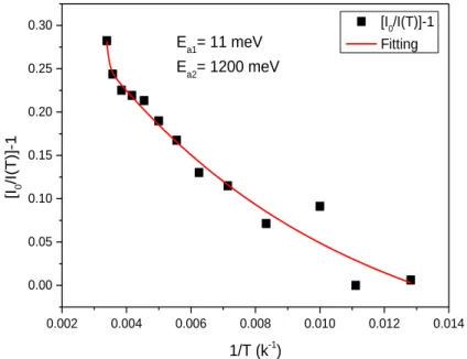
rapport O/N Un mécanisme permettant d’expliquer l’extinction de la luminescence avec la température est également proposé à partir des données de photoluminescence à basse température Les données ont été modélisées à partir de l’équation d’Arrhenius faisant intervenir deux fonctions exponentielles afin de déterminer l’énergie d’activation des processus mis en jeu Deux énergies d’activation de 475 et 35 5 meV ont été déterminées La première correspond à un phénomène d’ionisation thermique par transfert électronique depuis le niveau 5d2 de Ce3+ vers le minium de la bande de conduction. La seconde correspond à la
transition d’électrons de 5d1 vers 5d2 Finalement nous présentons une approche permettant d’obtenir une émission blanche observable à l’œil nu en ajustant les paramètres de dépôt Dans le cas des films dopés à l’ytterbium et des films co-dopés ytterbium-cérium, une excitation optique indirecte des ions Yb3+ émetteurs dans le proche infrarouge a pu être
obtenue et les mécanismes d’excitation de ions Yb émetteurs dans l’infrarouge sont discutés Une comparaison avec le comportement des films dopés au cérium est également proposée. La similarité des spectres d’excitation du cerium et de l’ytterbium s’accompagne de la possibilité de réaliser un transfert énergétique entre les deux ions au sein des films co-dopés. Ce transfert est mis en évidence par comparaison du comportement des films co-dopés et dopés avec uniquement de l’ytterbium ainsi qu’à partir du constat de l’augmentation des temps de montée et descente des signaux de photoluminescence résolue en temps. Nos
IX
résultats indiquent que le transfert énergétique est de type one-to-one down conversion et s’appuie vraisemblablement sur un mécanisme de transfert de charge Un mécanisme d’extinction de la photoluminescence de l’ytterbium activé thermiquement est proposé sur la base d’un échange d’énergie vers d’autres états luminescents peuplés thermiquement Dans le cas des échantillons d’Al(O)N dopés à l’ytterbium deux énergies d’activation Ea1=11.2 meV
et Ea1=1200meV peuvent être déduites de la modélisations des données de photoluminescence
résolues en température Par ailleurs, nous avons observé que l’énergie transférée entre la transition de plus forte énergie (1262 meV) parmi les pics désactivés thermiquement et les transitions activées thermiquement à 1274.6 meV (972.2 nm) et 2479 meV (500 nm) est de 12.2 et 1217 meV. Ces valeurs présentent un accord remarquable avec les valeurs de Ea1 et
Ea2, respectivement Ceci indique que la désactivation de l’émission par Yb3+ dans
l’infrarouge se fait par transfert énergétique vers les niveaux localisés à 500 et 972.2 nm. Dans le cas du dopage mixte avec Ce et Yb, l’émission par Yb3+dans le proche infrarouge est
caractérisée par une seule énergie d’activation proche de 28 5 meV La désexcitation de l’émission dans le proche infrarouge correspondant au pic localisé à 976 nm (1270 meV) peut ainsi être expliquée par la population d’un état radiatif émettant à 953 nm (1300 meV) Par ailleurs, la décroissance de l’émission dans le visible liée à Ce3+est caractérisée par deux
énergies d’activation, respectivement de 18 et 508 meV dont la somme (526 meV) est proche de l’énergie d’activation de 513 eV obtenue dans le cas des films présentant un dopage simple au cérium. Ainsi, nous pouvons considérer que le mécanisme de désexcitation thermique de la luminescence de Ce3+ intervient par transfert électronique de niveaux 5d excités du cérium vers la bande de conduction de la matrice que ce soit pour les échantillons dopés au cérium uniquement ou pour les échantillons co-dopés Ce, Yb.
Ce manuscrit est organisé en cinq chapitres et une conclusion générale comme suit :
Le chapitre un introduit les propriétés physiques, chimiques et optiques, la structure
cristalline et la structure électronique du nitrure d’aluminium Une brève description des défauts structuraux du nitrure d’aluminium et propose et les applications de ce matériaux sont mentionnées Les mécanismes d’excitation de la luminescence au sein d’AlN généralement proposés sont décrits à la fin de ce chapitre. Les propriétés des terres rares sont également présentées avec un intérêt particulier pour le cérium et l’ytterbium Les configurations électroniques des ions libres de ces terres rares sont alors introduites et leurs propriétés de luminescence généralement observées sont discutées ainsi que les mécanismes associés de transfert énergétique et d’excitation généralement proposés lorsque ces éléments sont placés
X
dans des matrices solides. Finalement, la nécessité de mener une étude sur les propriétés d’émission et d’excitation du cérium et de l’ytterbium dans AlN est motivée.
Le second chapitre décrit les méthodes et techniques expérimentales utilisées pour
synthétiser et caractériser les films d’AlN non dopés et dopés Ces méthodes sont détaillées en veillant à faire apparaître les principes fondamentaux et les caractéristiques utiles pour ce travail.
Le troisième chapitre présente et discute les résultats liés à la préparation des films d’AlN
non dopés et d’appliquent à sélectionner les conditions idéales de croissances des films utilisées pour le reste de l’étude Une attention particulière est portée sur l’optimisation des propriétés structurales et optiques. Un modèle de croissance est notamment proposé qui fait intervenir la manipulation de la mobilité des adatoms par l’intermédiaire de la teneur en azote dans la phase gazeuse et du flux d’atomes se condensant pour former les films
Le quatrième chapitre corrèle la luminescence aux propriétés microstructurales et chimiques
locales des films de nitrure d’aluminium dopés avec du cérium Il propose également des modèles permettant d’expliquer la luminescence de ce matériau, éventuellement applicables à d’autres matrices L’émission optique des films AlN et Al(O)N dopés au cérium est étudiée à partir de deux longueurs d’onde d’excitation Des mesures de PLE, de PL résolue en temps et en température sont présentées et analysées. La luminescence est également manipulée par l’intermédiaire de l’épaisseur des films et de la composition de la matrice, plus particulièrement du ratio O/N, de façon à obtenir de façon contrôlée des émissions bleue, verte et blanche.
Le cinquième chapitre vise à comprendre les mécanismes optiques dans les films de nitrure
d’aluminium co-dopés sur la base d’une étude comparative des films dopés au cérium et/ou à l’ytterbium La microstructure et la composition des échantillons préparés sont caractérisées et les propriétés optiques mesurées en utilisant la spectroscopie de photoluminescence à température ambiante, la PLE, la photoluminescence résolue en temps et thermiquement. Les mécanismes d’extinction de la photoluminescence de transfert énergétique entre le cérium et l’ytterbium ont notamment été mis en évidence en utilisant la photoluminescence à basse température et les mécanismes d’excitation ont été déterminés à partir de la PLE.
XI
Erweiterte Zusammenfassung
Dieses Projekt widmet sich der Untersuchung der optischen Eigenschaften von Seltenerd-dotierten Aluminiumnitrid-Dünnschichten. Insbesondere sollen die Lumineszenz mechanismen ausgewählter Seltenerdelemente in AlN-Dünnschichten untersucht werden. Die reaktive Magnetronsputter-Technik (RMS) wird verwendet, um die undotierten und dotierten AlN-Dünnschichten zu synthetisieren. Der Einfluss der Sputterbedingungen auf die Struktur und die optischen Eigenschaften der hergestellten Proben wird untersucht. Zusätzlich werden die optimalen experimentellen Bedingungen bestimmt, die während dieser Arbeit verwendet werden. Die Struktur- und Zusammensetzungsanalysen wurden mit verschiedenen Methoden wie Transmissionselektronenmikroskopie (TEM), energiedispersive Röntgenspektroskopie (EDS) und Rutherford-Rückstreu-Spektrometrie (RBS) durchgeführt. Die optischen Eigenschaften der Filme wurden durch Spektralphotometrie, Ellipsometrie und Photolumineszenz-Spektroskopie (PL) charakterisiert.
Für undotiertes AlN wurden gut kristallisierte AlN-Dünnschichten mit hohem c-Achsen-Orientierungsgrad hergestellt. Die bevorzugte Orientierung konnte durch das Einstellen des N2-Anteils in der Gasphase kontrolliert werden. Es wurde herausgefunden, dass die Synthese
von c-Achsen-orientiertem kristallinem AlN begünstigt wird, indem die Beschichtungen in einer stickstoffreichen reaktiven Umgebung abgeschieden werden. Die Ergebnisse wurden auf der Grundlage einer verbesserten Beweglichkeit von Adatomen interpretiert, die durch das Bombardieren der Filme mit schnellen Teilchen unterstützt wurde. Die optischen Konstanten (n, k) und die Bandlücke der hergestellten Filme wurden aus spektroskopischen Ellipsometriemessungen in Transmission und Reflexion modelliert. Es wurde gefunden, dass der Brechungsindex mit der Kristallorientierung abgestimmt werden kann, während die Bandlücke konstant gehalten wird. Unsere Ergebnisse legen nahe, dass die optischen Eigenschaften der AlN-Filme über ihre kristallographische Orientierung abgestimmt werden können, die wiederum durch die Menge an Stickstoff in der Gasphase variiert wird.
Für dotiertes AlN wurde kristallines Ce-dotiertes AlN hergestellt. Die Kristallstruktur der hergestellten Proben und deren Zusammensetzung wurde durch TEM-, RBS-, EDS- und EELS-Analysen untersucht. Es wurde herausgefunden, dass die Anwesenheit von Sauerstoff
XII
in diesem Material für die Sensibilisierung der Photolumineszenz wesentlich ist. Es hat sich herausgestellt, dass Sauerstoff nicht nur bei der Umwandlung von Ce-Ionen vom optisch inaktiven Zustand +4 zum optisch aktiven Zustand +3 eine wichtige Rolle spielt, sondern auch zur Bildung von Defektkomplexen mit Al-Leerstellen führt. Diese Defektkomplexe tragen zum Anregungsmechanismus von Ce-Ionen bei. Daher wurden optische Anregungs- und Emissionsmechanismen basierend auf der Rolle von Sauerstoff vorgeschlagen. Auf dieser Grundlage wurde eine Manipulation der PL erreicht und verschiedene Farben (blau und grün) wurden mit bloßem Auge deutlich beobachtet. Zusätzlich wurde ein Weißlichtemissionsansatz vorgestellt und ein starkes weißes Licht wurde beobachtet. Es werden Yb-dotierte und (Ce, Yb) co-dotierte Al(O)N-Systeme hergestellt. Die Kristallstrukturen und Zusammensetzungen der hergestellten Proben wurden untersucht. Es wird eine indirekte optische Anregung der NIR-Emission von Yb-Ionen erreicht. Die Anregungsmechanismen des NIR und die sichtbare Emission von einfach dotierten und co-dotierten Proben werden diskutiert. Es wurde herausgefunden, dass die Ähnlichkeit zwischen den PLE-Spektren von Ce und Yb ermöglicht, einen Energietransfer zwischen den zwei Ionen in dem Codotierungssystem zu erreichen. Die Art des Energietransfer mechanismus ist konsistent mit der Eins-zu-Eins-Abwärtsumwandlung über den Ladungsübertragungszustandsmechanismus. Die PL-Löschung wurde untersucht, indem die Entwicklung der PL mit niedrigen Temperaturen verfolgt wurde.
1
Motivation
Rare earth-doped III-V compounds attracted great attention since reported for the first time in 1980s as alternative solution to address the rare earth-doped silicon materials' drawbacks.[1] The small and indirect optical bandgap of silicon not only limits the choice of REs to those emit in IR region but also exhibits low luminescence efficiency due to the indirect bandgap feature of silicon. In contrast, III-V compounds in most cases show direct and large optical bandgap in the range 2 eV to 6 eV, providing good opportunity to host the RE ions emit in ultraviolet-visible (UV-Vis) range.[1] Also, it offers the possibility of integration with semiconductor microelectronics. Among III-V compounds, hexagonal wurtzite AlN exhibits the largest direct optical bandgap (6 eV). In addition, it shows very interesting chemical and physical properties such as strong chemical resistance and large thermal conductivity. Thus, it is a promising candidate for integration in devices working at high power operation.[2] Nevertheless, the optical mechanism of RE-doped AlN is still under debate, which motivates us to start this study in order to explore the optical behavior of this system. Hopefully, we can provide a significant contribution and enhance our understanding in this field.
This work, in general, is devoted to study the luminescence properties of selected RE elements incorporated in AlN thin film prepared by reactive magnetron sputtering as a candidate for lighting devices. More particularly, cerium (Ce) and ytterbium (Yb) ions have been selected as a case study in this thesis for two main reasons.
Firstly, from fundamental understanding point of view, Ce is the first lanthanides element
containing only one electron in the 4f orbital and its luminescence properties are characterized by f-d electronic transition. So, it is considered as an example for other RE ions that have the same kind of transition (Eu2+, Sm2+...). Yb is located at the end of lanthanides, and contains 13
electrons in the 4f orbital and its luminescent properties are mainly characterized by f-f transition (in Yb3+). It can be used as an example representing other REs that have the same
electronic transition. In addition, the f-d transition in Ce3+ is the outermost shell electronic
transition, while f-f transition in Yb3+ is lying in the core levels of valence electrons. This
makes the f-d transition is unshielded from the surrounding medium unlike f-f transition. This unshielded property of f-d transition results in strong influence of the local environment on the luminescence of Ce3+. Whereas, the shielded property of f-f transition in Yb3+ significantly
2
ions are expected to be different. Therefore, by studying and comparing the luminescence properties of Ce3+ and Yb3+, we will have the chance to test two different electronic transitions in AlN. Moreover, Ce ions emit in the UV-Vis light spectrum, while Yb3+ ions emit in NIR. Hence, large part of light spectrum can be covered within this work.
Secondly, from application point of view, Ce3+ ions are used to produce blue light in order to
fabricate blue or white light emitting devices. It is also very useful in scintillation and thin film flat panel light devices (TFFPLD) fields. On the other hand, Yb attracts a lot of attention in photonic systems mainly based on light confinement (e.g. planar, waveguide optical fibers and lasers). Thanks to the high AlN refractive index, about 2.1, it is expected to enhance the confinement efficiency of Yb based devices integrated in AlN. Moreover, AlN as a III-V compound is excellent to match with the silicon technology, which is additional advantage for silicon integration technology approaches. Furthermore, the piezoelectric properties of AlN open a promising way for realizing piezo-phototronic integrated chips technology. Hopefully our study of Ce and Yb doped in AlN will drop new and important seed in this regard.
This manuscript is organized into five chapters and general conclusion as follows:
Chapter one: is a general introduction about the basic physical, chemical and optical
properties of AlN and rare earth with particular focusing on Ce and Yb-doped AlN. The crystal and electronic structure of AlN are described. Brief section about the structure defects in AlN is stated. In addition, some AlN applications are mentioned. Regarding the RE ions, the electronic configurations of the free ions are described. Also, a brief introduction about the luminescence, energy transfer, excitation mechanisms of RE in solid hosts will be provided. At the end of this chapter, description of the types of the excitation mechanisms in AlN is explained. Finally, the importance of studying Ce and Yb in AlN systems will be highlighted.
Chapter two: is dealing with the experimental methods and techniques that have been used in
preparation and characterization of our samples.
Chapter three: is devoting to the results and discussion of the prepared AlN films and
selecting the optimum experimental condition for the doping step. More precisely, the structure and the optical properties of AlN thin film prepared by reactive magnetron sputtering technique are examined. The correlation between the sputtering conditions, the crystallographic orientation, the morphology, the microstructure and the optical properties
3
will be presented. The optimum experimental conditions that will be used during this work are discussed. Finally, chapter's conclusion has been stated.
Chapter four: shows the result and discussion of prepared Ce-doped AlN films at different
conditions and the correlation of the microstructure with the luminescence properties. It also provides a significant guideline for understanding the optical behavior of such material. The optical response of Ce-doped AlN and Cerium doped aluminum (oxy)nitride (Ce-doped Al(O)N) has been examined by photoluminescence (PL) under optical excitation with different wavelengths. The photoluminescence excitation measurements (PLE) have been performed in order to explore the excitation mechanisms. In addition, the PL intensity evolution with low temperature variation was used to gain more information about the PL thermal quenching mechanisms. A comprehensive study is presented to understand the optical mechanisms of Ce doped aluminum nitride and aluminum (oxy) nitride materials. Based on the proposed approach, PL manipulation has been achieved offering different emission colors (blue, green and white) that can be used as candidates for lightening applications.
Chapter five: is dedicated to understand the optical mechanisms of Yb-doped AlN and (Ce,
Yb) co-doped AlN samples. The main goal of this part of the work is to establish a comparative study between two different rare earth ions doped AlN in order to explore the similarities and the discrepancies, particularly in the optical behaviors. The microstructure and the compositions of the prepared samples have been investigated. The optical properties have been also examined using the steady state PL at room temperature, PLE, and time resolve photoluminescence (TRPL). The PL thermal quenching mechanism for Yb and (Ce, Yb) co-doped AlN is presented by probing the PL evolution at low temperatures. In addition, energy transfer (ET) mechanism between Ce and Yb has been established.
4
Chapter I
General Introduction
In this chapter, a general introduction about the basic characteristics of aluminum nitride (AlN) and rare earth elements (REs) is presented. We will focus and highlight on the properties relevant to this study and used in our results' interpretations and discussion. This chapter is classified as follows; the first part is dealing with AlN related features; crystal and electronic structures, types of defects, preparation methods and applications. Secondly, it is focusing on some luminescence issues related to REs (electronic transitions, energy transfer and...etc). After that, general discussion about the optical behavior of REs-doped semiconductors is given. Finally, a survey on the application of Ce and Yb-doped AlN is presented.
1.1- Aluminum nitride (AlN): Basic properties
AlN is a III-V compound and crystallizes in the hexagonal wurtzite structure where each Al atom is tetrahedrally connected to the nitrogen atoms by covalent bonds. This particular crystal structure of AlN exhibits high chemical and thermal stabilities, high hardness and large thermal conductivity and melting temperature of 2200 oC.[2] It also shows a remarkable high optical bandgap of 6.2 eV. All these promising features allow AlN falling under intense research activities. During the last decade, several works have been dedicated to exploit the excellent properties of AlN to put it directly in the industrial field. On the one hand, many potentials have been reported on different synthesis methods in order to obtain well crystalline AlN in bulk,[3] thin films,[2] and even in nanopowders forms.[4] On the other hand great efforts have been spent to characterize and understand the chemical and physical properties of AlN in order to serve the technological development especially in acoustic [5-6] and optoelectronic fields.[7-8] In the following sections, a background required to get through this work is discussed.
1.1.1- AlN crystal structure
AlN belongs to the III-nitrides group which includes the compounds consisting of nitrogen with the elements of column III in the periodic table. Terminologically, III-nitrides usually point to GaN, InN, AlN and their alloys InGaN, AlGaN, AlInN, and AlInGaN, which are the most important compounds obtained from this group in semiconductor technology. These
5
compounds are found in wurtzite (WZ), zinc blende (ZB) and rocksalt atomic structures.[9] AlN exists in WZ and ZB, however the WZ structure is more stable than ZB. The main difference between WZ and ZB structures in AlN is the ions stacking sequence inside the crystal lattice.[10] Specifically, hexagonal WZ-AlN (H-WZ) structure is the stable and the easy growing one under normal conditions. Fig (1.1) shows the crystal structure of hexagonal WZ-AlN.
Fig. (1.1): Crystal structure of wurtzite AlN.[11]
The average lattice parameters of hexagonal wurtzite AlN a= 3.11 Å and c= 4.98 Å are mainly depending on the lattice strains and the oxygen content, which is an unavoidable contamination. The ideal c/a ratio for wurtzite structure is 1.63 with an internal coordinate
u=(a/c)2 =0.375.[9] It was found that the specific stacking sequence of hexagonal w-AlN
result in attracting pairs of cations and anions by electrostatic forces.[9] These electrostatic forces lead to decrease the c/a ratio and promote the ionic character of AlN, which makes the WZ phase more stable than the ZB. As a result, an internal spontaneous polarizability is initiated inside AlN crystal lattice. This spontaneous polarizability is the key point behind using AlN crystals in the piezoelectricity field. Furthermore, the difference between the lattice parameters (c and a) results in an anisotropic property along each axis. For instance, the ordinary and the extraordinary refractive index of AlN are not the same, which is an important property in the field of microchips nonlinear optics.[12]
The lattice structure of w-AlN consists of tetrahedron units where each Al atom is connected with four N-atoms by two kinds of bonds, sometimes referred as B1 and B2. B2 bonds are parallel to the c-axis while B1 bond are the other three legs in the tetrahedron terminals as shown fig. (1.1). In addition, the bond length of B2 (0.1917 nm) is longer than B1 (0.1885 nm).[13] Al and N atoms form four sp3 hybridization orbitals in the crystalline structure. The
6
outer shell of Al atoms consist of 4 orbitals (3s2 3p1) and the outer shell of N atoms contain 4
orbitals (2s2 2p3) with electronic configuration as shown in fig (1.2). In AlN, Al atoms share
its outer shell 3 electrons with the 2p orbital in N atoms to compose the three B1 bonds, which are more covalent in nature. While the B2 bond is formed from coupling an empty orbital of Al atom with the full 3s orbital in N atom (lone pair electrons). This displays some ionic characters to this B2 bond.[14]
Fig (1.2): Schematic diagram of the electronic configuration of Al and N atoms.
1.1.2-Electronic structure of AlN
The band structure
The electronic structure of semiconductor material is mainly governed by the bonding system and the crystal structure of the material.[15] Wurtzite AlN is considered as a direct bandgap, whose band edge is located at the Γ point, see fig (1 3)
7
Large direct bandgap can be realized between the minimum of the conduction band and the maximum of the valence band to reach to 6.2 eV in crystalline w-AlN. This bandgap makes AlN a promising material to host emitting centers with light emission in UV-Vis ranges with low thermal quenching of the luminescence. In addition, the direct feature of this band structure maximizes the benefit from the excitation energy avoiding any phonon consumption that occurs in other indirect bandgap semiconductors e.g. Silicon.
The density of states (DOS)
The partial density of states (DOS) of w-AlN is presented in fig (1.4). It can be observed that the valance band formed by two sub-bands of N atoms 2s and 2p, while conduction band raises from hybridization of the s and p orbitals of the Al atoms. [17-18]
Fig (1.4): the partial and total DOS of w-AlN.[17]
The optical- Phonon frequencies
Studying the optical phonons of AlN is of great interest due to its application in optoelectronic field. Complementary measurements of Raman and FTIR have been used to obtain the full information about the optical phonons. AlN with wurtzite structure exhibits six optical phonon modes[19-20] classified as shown in fig (1.5). As it has large number of atoms, the analysis of the optical phonons is complex, however the representation at the point Γ is reducible into Γ= A1+E1+2E2+2B1; A1 and E1 are Raman and IR active, 2E2 branches are
8
Raman active only while B1 branches are inactive (forbidden in Raman and IR). The phonon frequencies are listed in below table (1.1).[19] However, it can be shifted and/or broadened depending on the microstructure (crystal or amorphous), the lattice strain and the impurities in particular the oxygen contamination.[21] That is why Raman and FTIR can be used as a tool to give information about the degree of disorder and the lattice strain of a given material.[22]
Fig (1.5): Schematic diagram for the optical phonon modes of w-AlN.[19]
Table (1.1): The optical phonon modes values in w-AlN compared to several other works from [19] and the references wherein.
For instance, Khan, S., et al.[23] showed how the FTIR and the Raman modes of nanocrystalline AlN can be modified by the experimental conditions and used as tools reflecting the microstructure picture. In the same line, Jagannadham, K., et al.[24] displayed the use of relative intensity of phonon peaks associated to the crystalline and amorphous phases to identify the volume fraction of the amorphous phase. They also referred the shift of the peaks in FTIR to the residual stress. Moreover, according to [25], The ratio of integrated
9
areas of A1(TO) and E1(TO) absorption bands in FTIR can be related to the degree of preferential orientation of AlN thin film.
1.1.3- Type of defects in AlN
AlN, like any semiconductor materials can't be formed without avoiding defects in its structure. The word defect is used here to point to imperfection in the crystalline material that interrupts the regular pattern of the material crystallography. This interruption locally alters the atomic and the electronic structure and results in modifications in the macroscopic properties of such material. The type and density of the defects depend mainly on the preparation methods and conditions. The functional properties and the electronic structure of semiconductor devices critically rely on the type of these defects. Therefore, controlling the performances of such devices can be achieved by understanding and managing the native and impurities defects. It has been reported that the type of defects can be classified into[26]: point defects (e.g. vacancies, interstitial and anti-sites), line defects (e.g. dislocations), planar defects (e.g. grain boundaries) and Bulk defects (e.g. pores, cracks and voids). Line, planar and bulk defects can be strongly minimized and avoided by taking care and optimizing the experimental conditions. However, the point defects as well as some impurities can't be totally avoided. Thus, it is of great importance to understand their behavior. It has been noticed that the existence of point defects/impurities to certain limit is not detrimental. In contrast, in some cases, the defects are intentionally added to the semiconductor materials to enhance a desired functional property. For example, small amount of boron or phosphorous impurities are added to pure silicon to increase the concentration of the charge carriers (holes or electrons respectively) and improve the electric conductivity of silicon.[27-28] Alternatively, generation of point defects can be used as a mediator to transfer the energy, radiatively or nonradiatively, to optically activate rare earth ions inside semiconductor. Hence, the optical properties can be enhanced.[29-30] Therefore, understanding the behavior of defects opens the door to control and tailor the material properties.
More precisely, the effect of point defects and their complexes in AlN on electronic and atomic structures have been extensively studied.[31] Stampfl et al used the density functional pseudoptential method calculations to investigate the native and impurities defects in AlN. The formation energy and the charges of the defects have been considered during their study. They found that the most pronounced native defects that have lowest formation energy in n-type and p-n-type AlN are VAl and VN especially the triply negatively and triply positively
10
charged; respectively. In wurtzite AlN, VAl acts as an acceptor center near the valance band
maximum (VBM) while VN acts as a deep donor level below the conduction band minimum.
In addition, the authors also demonstrated that both kind of defects induce the same geometrical interruption in the atomic structure that leads to outward moving for the nearest neighboring atoms with different percentage from the ideal position depending on the defect charge state. Moreover, the two defects act as compensation centers that prevent to achieve successful n-type or p-type doping. Regarding the impurities defects, the dominant unintentional impurity in AlN is Oxygen. It was found that oxygen in AlN matrix substitutes nitrogen site to form ON+ defect that has low formation energy. In addition, when O-atoms
incorporated inside AlN, each 3 O-atoms that substitute N-atoms generate one Al vacancy (VAl), since they enter as (VAl Al2 O3) phase. After that, the two defects VAl and ON form an
energetically favorable defect complex (VAl-ON)2-/-.[32-33] There are many reports on the
influence of oxygen in AlN on the optical properties of AlN. For instant, G. A. Slacket al [34] reported on how the oxygen concentration can influence on the optical and thermal conductivity of AlN material. It is found that understanding the behavior of such oxygen related defects is essential for manipulating the properties of AlN, in particular the optical response.
1.1.4- AlN: Preparation methods
There are many growth methods that can be used to prepare AlN thin films. Researchers everywhere have screened several techniques in order to study the different growth mechanisms and the correlation with the functional properties of AlN. For instance, the most common methods are pulsed laser deposition (PLD)[35-36], chemical vapor deposition (CVD)[37] and physical vapor deposition (PVD).[38] Within PVD method, reactive magnetron sputtering (RMS) attracted more attention particularly in the industrial field thanks to its low cost, simplicity, large scale production applicability, and the high quality of coatings that can be achieved at low temperature.[39] More about reactive magnetron sputtering technique and how it works will be addressed in details in the experimental chapter.
1.1.5- AlN: Applications
Thanks to the physical, chemical, mechanical and optical properties of AlN, many applications can be found. For instance, AlN shows excellent acoustic properties due to its high piezoelectric coefficients, in particular d33, that provide a chance to enhance the
11
bandgap of AlN of 6.2 eV allows emission of a deep UV wavelength around 200 nm to be obtained. Indeed, an AlN LED with emission of 210 nm has already been reported.[40] Moreover, the high thermal conductivity of AlN, about 300 [41] and 130 W/mK [2] in bulk and thin film respectively, is of particular interest in high temperature working devices. Furthermore, manipulation of optical properties of this optically transparent material represents an important challenge for future applications, especially in optical quantum circuits. Three functional properties are of primary importance for this purpose. First, c-axis out of plane orientation of AlN thin film is essential for exploiting its largest second order nonlinearity for wavelength conversion and electro-optical effects. Second, the high ordinary refractive index (typically 2.1) of AlN deposited on Si wafer is a prerequisite for realizing low loss in silicon integrated AlN photonic circuits.[42] This high refractive index allows to strongly confine the light for long distance leading to emergence a non-linear optical effect on chip scale.[12] Third, the wide range of AlN transparency (bandgap close to 6 eV) can be exploited for wide operation band devices from UV to IR wavelengths. Combining the above features together make AlN an excellent candidate for integrated nonlinear optics. Exploiting the high transparency in UV-visible range of AlN combined with its dielectric properties, make AlN is an excellent host material for transition and rare earth elements for magnetic and optical investigations. Therefore, the following sections will be dedicated to the characteristics of doped AlN.
2.1-Rare-earth elements
The name rare-earth consists of two parts; the first part rare refers to the difficulty to find these elements in pure minerals or free metals phases not to its relative abundances in the earth's crust. It is more abundant than silver and lead. In addition, these materials co-exist in oxides which indicate the difficulty to separate them from each other. This is the meaning of the second part of the name; earth, where the Greeks defined earth as the material that couldn't be further changed by heat.[43]
2.1.1- Electronic structure and transitions of REs
Rare-earth metals defined as the 15 lanthanides located below the main body of the periodic table plus Scandium and Yttrium elements as shown in fig. (1.6).
12
Fig (1.6): The periodic table.[43]
These lanthanide elements are characterized by occupancy of the 4f level by electrons (from 0 in La to 14 in Lu). The properties that depend mainly on the occupancy of 4f level make the interest of lanthanides. Although, the term Lanthanides in general is restricted to the 14 elements from Ce to Lu that contain partially or totally filled 4f electrons, Scandium (Sc), Yttrium (Y) and lanthanum (La) can be considered in the same group. They exhibit similar chemical and physical properties to the 14 lanthanides elements although they haven't any electrons in the 4f level. The reason behind joining these three elements is the analogy of their electronic configuration of the outer shell three electrons with the lanthanides; (3 d 4s)3 for
Sc, (4 d 5 s)3 for Y and (5d 6 s)3 for La. Thus, it shares all the lanthanides properties that are
not depend on the 4f electrons. As we are interested in this work by the optical properties of cerium and ytterbium, we will focus our attention on the properties of the 14 lanthanides elements that contain electrons in its f orbital.[44] Although, the lanthanide elements have similar basic electronic structures, the small differences between the individual elements result in diversity in their properties, in particular the optical behaviors. Therefore, in order to understand the basic characteristics of lanthanides, the electronic configuration should be considered. In the following table (1.2), all the lanthanides' electronic configurations in metallic and ionic forms have been stated.
13
Table (1.2): Lanthanides electronic configuration of the metal and the valence states +3,+4,+2.[45]
It is noticed that all the lanthanides share the xenon core electrons’ configuration Then, the rest of electrons are placed in 6s and 4f orbitals except four elements, namely La, Ce, Gd and Lu that sharing one electron in the d orbital lead to more energetic stability and result in empty 4f (La), half-filled 4f (Gd) and fully-filled 4f (Lu). The filling sequence of electrons from La to Lu in the outer-shells follows energetic stability concept. In addition, It was found that 4f electrons are spatially localized lying in the core of the REs while 5s and 5p orbitals are spatially extended, see for example fig (1.7) for Gd.[44]
14
In addition, the filled 5s and 5p outer shells are efficiently shield the 4f electrons from the surrounding ligands result in weak crystal field strength that can be strongly perturbed the 4f states. Moreover, this shielding property results in the f orbitals don’t participate in the formation of valence bonds, hence the valence of REs is determined by s and p orbitals.[46] As a consequence, f-f absorption spectra are very narrow which raises questions about the lanthanides' energy levels. It is worth noting that 4f-4f transition are exhibiting electric dipole transition although its parity is forbidden.[47-48] There are experimental evidences showing that the 4f-4f transition strongly matches with the electric dipole transition principle. Therefore, Judd[47] and Ofelt [48] reported that there is a probability of mixing states with the higher electronic levels of opposite parity (e.g. d-orbital). This arises from the asymmetric local environment around the RE results in perturbation in the crystal field that lead to partially allowed the electric dipole of these transitions. As a consequence, models for the 4f energy levels transitions became necessary. The most effective model used up to date was reported by Dieke [49] and is called Dieke diagram, provides the energy of the sub-splitting levels of RE3+ in different matrices. Hence, the origin of the electronic transition of
lanthanides has been addressed and matched with the experimental luminescence results obtained from these ions.
In the following section some general basic concepts about the luminescence will be given before getting through the luminescence characteristics of lanthanides.
2.1.2- Luminescence principles
Terminology
The difference between the common terms luminescence and incandescence is that, both are refereeing to emission of light but luminescence is related to emission of light from a cold body while incandescence is related to hot body (like sun or tungsten lamp). Hence, a cold body can be undergo luminescence process if stimulated by any means (except heat) to emit light. This stimulation process is called excitation. As a result, the type of luminescence action is classified according to the kind of excitation process. For example, the excitation can be performed by light (Photoluminescence), injection of electric current (Electroluminescence), bombardment of electron (Cathodoluminescence), bombardment by ionizing radiation (Radioluminescence), chemical reaction (Chemoluminescence) or by mechanical stress (Triboluminescence)...etc.[50] Therefore, the excitation process determines the type of
15
luminescence as well as the mechanism by which the light is emitted. The following section is focused on the photoluminescence process as it is the main subject of this work.
Photoluminescence (PL)
PL is the most popular method for obtaining light from a luminescent material and usually divides into two main categories: fluorescence and phosphorescence.[51] Both are concerning to light emission from a sample after absorbing (excitation by) light, but the main different between them is the decay time, i.e. how long time takes between the excitation and emission. Phosphorescence is a slower process than fluorescence. The reason behind the difference in the time scale between the two processes is the occupancy of forbidden state by the excited electron in the case of phosphorescence materials. Fig (1.8) shows a schematic diagram illustrates the two processes.
Fig (1.8): Schematic diagram revealing the absorption, fluorescence and phosphorescence process.
Luminescent materials should be excited by absorbing energy equal to the energy difference between the ground and excited state. In case of fluorescence, a deactivation (relaxation) process occurs from the excited singlet state to the ground singlet state (spin allowed process i.e. S1, 2 states to S0). In contrast, phosphorescence is a transition from excited triplet state to
the singlet ground state after a non-radiative intersystem crossing process. That is why phosphorescence process takes longer time.[52] The probability of which process is dominating or which mechanism will be followed by the substance mainly depends on the electronic structure of the material and how it can be modified under the experimental conditions. Since, the luminescence properties are strongly dependent on the electronic structure for each material. So, the luminescence characteristics are unique property for each
16
substance. Therefore, one can find a group of elements that share the same electronic structure having quite similar luminescence properties. This is the case of our study on lanthanides. As mentioned before, all Lanthanides have similar electronic structure except the slight differences of Ce, Gd and Lu. Also, all the RE3+ ions- the most stable valence state- exhibit luminescence through f-f transitions except Ce3+ that shows f-d transition. There are other
elements like Eu2+, Yb2+ and Sm2+ with stable +2 state exhibiting f-d transitions under certain conditions. Thus, Ce3+ is a unique RE3+ with luminescence properties originated from the f-d
transition.
Luminescence mechanism
As seen in the previous section, how luminescence takes place, is very simple way as follows: the radiation absorbed by the material under investigation results in excitation of its electrons to excited states. Then after a certain characteristic time (excited state lifetime) it returns to the ground state by losing the absorbed energy through radiative process (emission) and/or nonradiative process (heat). The competition between the radiative and nonradiative processes determines the luminescence efficiency of the emitting species. However, finding and understanding the correct mechanism explaining how a specific emitting center (activators like REs, transition metals or even semiconductors materials) behaves and emits light is quite complicated. Many parameters should be considered to study a luminescent material. Some of these parameters are basic like the excitation spectra, radiative and nonradiative probabilities, the absorption cross section, the lifetime of the excited states and the energy transfer mechanisms For example, in some cases the activator doesn’t absorb the excitation energy directly but via different indirect ways. For instance, energy transfer process is the well established mechanism used to excite some activators indirectly. In such systems, another species called sensitizer (S) (sometimes the host material or another ions) is responsible to absorb then transfer the excitation energy to the activator (A) that , in turn, emits the light, as shown in the simple schematic diagram fig (1.9). This illustrates the rather complicated nature of the luminescence process. It is essential to understand the physical role of the above processes in order to explain the luminescence results. Particularly with REs, It was found that the luminescence of most of lanthanides comes from the partially allowed electric dipole 4f-4f transitions which are shielded by the outermost valence orbitals as mentioned in (beginning of rare earth section).This results in very weak direct absorption cross section of these ions. Hence, another indirect excitation method is needed.
17
Fig (1.9): schematic diagram illustrates the energy transfer process from sensitizer to activator.
For this reason, in order to efficiently excite the lanthanides, another species is required to absorb the excitation energy and transfer it to the lanthanides ions. This process is called "sensitization" and the species used for the energy transfer is called "sensitizer" (energy donor) while the emitting lanthanide ion is called "activator" (energy acceptor).
The energy transfer mechanism is the most acceptable process used to explain the indirect excitation of rare earth ions doped in different hosts. Therefore, a brief introduction about the energy transfer phenomenon is given in the following section.
Energy transfer mechanisms
Two energy transfer mechanisms are proposed for donor-acceptor energy transfer, the Dexter and Förster energy transfer mechanism.[53-54] In the case of Dexter mechanism, the energy is transferred via electrons exchange between the donor and acceptor. The electron in the excited state of the donor can be exchanged by one in the ground state of the acceptor, resulting in excited acceptor. In other word, the electron in the excited donor hops to the excited state of the acceptor result in excited acceptor and an electron from the ground state of the acceptor hops to the ground state of the donor.
In this case of Förster energy transfer, the energy is transferred from the excited donor to the acceptor nonradiatively via dipole coupling. Figure (1.10), illustrates the two kinds of mechanisms. It is worth mentioning that both mechanisms are mainly depending on the spectral overlapping and the inter-distance between the donor and the acceptor.
18
Fig (1.10): Schematic diagram for the Forster and Dexter energy transfer.
Luminescence decay rates
One of important characteristic emission features is the luminescence deactivation (decay) rate. According to the quantum mechanics theory, it is noticed that the luminescence loses its intensity spontaneously after the excitation and returns back to the ground state after certain time. This process, called the luminescence decay rate, is characteristic for each luminescent species and brings many information about the excited level and the way this level deactivates.[55] As there are two pathways for a substance to deactivate the excited state either radiatively and/or nonradiatively, knowing the decay rate can lead to estimate the quantum efficiency of the material as well as the energy transfer efficiency if any. One popular way to figure out the decay rate is the time resolved photoluminescence experiment (TRPL). In this case, the evolution of the PL intensity is recorded as a function of time after pulse excitation. After that, by fitting the experimental results of the TRPL, the deactivation constant corresponding to the observed decay rate (called the total decay rate ktot) can be
estimated. The total decay rate is considered as a summation of the radiative krad and the
nonradiative decay knonrad, as in the equation (1.1),[55]
ktot= krad. + knonrad.,
(1.1)
The radiative decay rate can be calculated by solving the rate equation of the spontaneous emission.[55] Then, the nonradiative decay rate can be estimated. The quantum efficiency QE of the emitting material, which is the relative amount of emitting photons to the absorbed photons, can be calculated using the following equation;[55]
QE= krad/( krad+ knonrad), (1.2)
19
After the above information about the basic characteristics of the luminescence process, in the following we are going to focus on the REs behavior as luminescence centers in solid hosts.
2.1.3- Rare earth doped in solid hosts (semiconductor/insulators)
Rare earth-doped solid hosts attract great attention from luminescence devices point of view by combining the luminescence properties of REs with the electronic features of the host matrix. It also attracts a particular interest in the field of integrated optoelectronic devices. Rare earth based-devices have extended to cover many sectors from energy harvesting (e.g. solar cell) moving on telecommunications to lighting devices (e.g. lasers and displaying units). Although, the trivalent REs are of a great technological interest due to their sharp emission lines, some divalent REs ions that exhibit broad emission (e.g. Sm+2 and Eu+2) find
their way to the devices required broad band emission such as w-LEDs. As consequence of shielding the 4f electrons by 5s and 5p electrons, it is believed that the electronic energy levels of the 4f are influenced mainly by the spin-orbit interaction while the electron phonon coupling with the host becomes weak. Nevertheless, the energy levels of intra-f electrons have been found slightly affected by the applied crystal field.[30] For instance, this can be observed in the difference of the emission lines and photoluminescence excitation of Er doped hexagonal and cubic GaN, which referred to the difference in the local symmetry around Er ions.[56]Hence one can conclude that, although the strong shielding of the intra-f electrons of the REs, the significant influence of change in the local environment around it cannot be excluded.
2.1.4- Issues related to the luminescence of RE-doped solids
Beside the luminescence behavior, incorporation of rare earth in solid hosts raises some key questions about the lattice location of the RE inside the host and the kind of interaction with the host material. In the following section some of these points will be briefly covered.
RE site location in the host lattice structure
As mentioned before, the local environment around the RE in the host material can induce modifications in the electronic structure of the RE. These modifications, sometimes, are of great importance such that it can modify the optical response of the RE by altering the transition probabilities of the electronic levels. For example, Steckl, A.J. et al[57-58], demonstrated how the Eu lattice site can play a role in changing the emission wavelength,
![Table (1.1): The optical phonon modes values in w-AlN compared to several other works from [19] and the references wherein](https://thumb-eu.123doks.com/thumbv2/123doknet/14715311.749890/26.892.273.615.283.618/table-optical-phonon-modes-values-compared-works-references.webp)