Absence of boron aggregates in superconducting silicon confirmed by atom probe tomography
5
0
0
Texte intégral
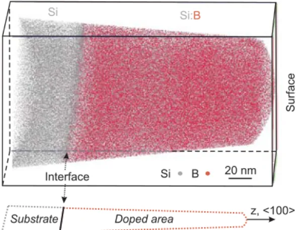
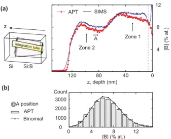
Figure
Documents relatifs