HAL Id: hal-01598160
https://hal.archives-ouvertes.fr/hal-01598160
Submitted on 29 Sep 2017HAL is a multi-disciplinary open access archive for the deposit and dissemination of sci-entific research documents, whether they are pub-lished or not. The documents may come from teaching and research institutions in France or
L’archive ouverte pluridisciplinaire HAL, est destinée au dépôt et à la diffusion de documents scientifiques de niveau recherche, publiés ou non, émanant des établissements d’enseignement et de recherche français ou étrangers, des laboratoires
Encounter on Advanced Materials Materials
Pierre Saint-Grégoire
To cite this version:
Pierre Saint-Grégoire. Materials and Devices CONFERENCE VOLUME Communications pre-sented at the First Transpyrenean Encounter on Advanced Materials Materials. France. 2017, �10.23647/ca.md20170407�. �hal-01598160�
Materials
Materials
and
and
Devices
Devices
CONFERENCE VOLUME
CONFERENCE VOLUME
Communications presented at the First
Communications presented at the First
Transpyrenean Encounter on Advanced
Transpyrenean Encounter on Advanced
Materials
Materials
(TEAM1 – Sète, 4,5,6 july 2017)
(TEAM1 – Sète, 4,5,6 july 2017)
Editor P. Saint-Grégoire
Editor P. Saint-Grégoire
Published by Collaborating
Published by Collaborating
Academics
Academics
http://co-ac.com
http://co-ac.com
Materials and Devices, Vol.2, No2 (2017)
An international research journal
General informations
Materials and Devices is a new journal devoted to all aspects of materials and related devices. It is Open Access and free of charges for authors.
Our aim was to create a high quality journal, with a strict peer-review process, and complying with the transparency rules edicted by the DOAJ, COPE,...
Materials and Devices publishes several types of articles :
- A : regular papers, that should present the results of original research, not published or submitted somewhere else. - L : short papers, written as letters, focusing on one or few particular aspects, representing a very significant progress, for rapid publication.
- R : review papers, that presents a summary of results published in literature, on fields covered by the journal.
- T : technical papers, on the development of laboratory technics and aparatus relevant to studies on materials and related devices. Such papers will present the details of the designed technics, and an example of application in real condition.
- Ur : Unexpected and « negative » results, the journal accepts papers describing unexpected results, or results considered as negative, provided that the original ground arguments are sound, and that a reasonable interpretation can be proposed. Typical examples are : a synthesis process that is generally successful, which aborts in given cases, or give different unexpected but interesting results, results contradicting a theory or a model, etc. The idea to publish such papers is mainly to save time to the scientific community by giving information that is generally not available, except as private communications between researchers.
We are happy to announce these innovations : Section T (technical papers) and Ur (Unexpected and « negative » results are original. They correspond to needs in the scientific community.
- Conf: conference papers : Finally, Materials and Devices may also publish conference proceedings and conference papers in special volumes. This service is not free, organizers of conference interested should contact the journal to know details.
Aims and scope of the journal The topics covered by the journal are wide, it aims at publishing papers on :
- all aspects related to materials, namely according to their chemical formula (oxides, fluorides, carbon compounds, …, organic, inorganic), to their physical properties (conductors, super-conductors, semi-conductors, insulators, dielectrics,...), to their nature (crystalline or amorphous materials, liquid crystals, modulated systems, aperiodic materials, nanomaterials and nanostructured materials)… or environmental type (ecomaterials), or according to some specific applications. Papers on biomaterials, geomaterials, archeomaterials or on studies of ancient materials are also welcome. A particular attention is also paid on environmental studies related with materials. Authors are also encouraged to submit papers on theoretical studies applied to materials, including pure mathematical approaches, physical approaches, models, numerical simulations, etc.
- devices in a wide sense. However, concerning Devices, the scope is restricted to those integrating particular materials (for instance memories based on some specific magnetic materials) or category of materials. Papers on all types of such devices are welcome.
published article can be freely downloaded, and self archiving of your paper is allowed!
We apply « the principles of transparency and best practice in scholarly
publishing » as defined by the Committee on Publication Ethics (COPE), the Directory of Open Access Journals (DOAJ),
and the Open Access Scholarly Publishers Organization (OASPA). The journal has thus been worked out in such a way as complying with the requirements issued by OASPA and DOAJ in order to apply to these organizations.
Evaluation – peer-reviewing : After reception, the paper is sent to two reviewers for evaluation. In case of divergent
opinions of reviewers, the editor-in-chief sends the paper to a third reviewer and then gives a final decision based on all reports. Reviewers are asked to reply within three weeks to warranty a fast publication process.
Copyright on any article in Materials and Devices is retained by the author(s) under the Creative Commons (Attribution-NonCommercial-NoDerivatives 4.0 International (CC BY-NC-ND 4.0)), which is favourable to authors.
(*) An open access journal means that all content is freely available without charge to the user or his/her institution. Users are allowed to read, download, copy, distribute, print, search, or link to the full texts of the articles in this journal without asking prior permission from the publisher or the author. This is in accordance with the BOAI definition of open access.
International editorial board
Orientation of the journal, choice of reviewers, special issues, editorial policy, etc, are discussed by the international editorial board.
List of members
Algeria
Mokhtar BOUDISSA, Professor Researcher, Dpt EBT, ENMC Laboratory, Faculté de Technologie, Université F. Abbas
SETIF-1, Sétif 19000 - boudi44 @ yahoo.fr
Brazil
Paulo T.C. FREIRE, Full professor, Universidade Federal do Ceará, Fortaleza - tarso @ fisica.ufc.br
José DE LOS SANTOS GUERRA, Professor, Instituto de Física, Universidade Federal de Uberlandia (UFU),
Uberlandia – jsantosguerra @ gmail.com
Burkina faso
Dieudonné Joseph BATHIEBO, Full professor, University of Ouagadougou –
[email protected]
CanadaZuo-Guang YE, Professor, Simon Fraser University, Burnaby, BC - zye @ sfu.ca Cuba
Aimé PELÁIZ BARRANCO, Full professor, Physics Faculty, Havana University - [email protected] Maria SÁNCHEZ, Full professor, Faculty of Physics, University of Havana – maruchy @ fisica.uh.cu
Elena VIGIL, Full professor, Physics Fac. - Materials Sc. & Tech. Inst. (IMRE), University of La Habana, and Solar
Energy Cathedra Chairperson, Cubasolar-U.H. - evigil @ fisica.uh.cu
Czech Republic
Ivan GREGORA, Institute of Physics, Czech Academy of Science, Prague - [email protected] Vacláv JANOVEC, emeritus professor, Prague
Denmark
Heloisa BORDALLO, Associate Professor, Niels Bohr Institute - University of Copenhagen France
Patrice BOURSON, Professor, LMOPS Université de Lorraine - Centralesupelec 2 rue E. Belin 57070 Metz -
Pierre SAINT-GRÉGOIRE, Full professor, Universities of Toulon and Nîmes,
president of Collaborating Academics, https://fr.linkedin.com/in/saint-gregoire-pierre-5bb6372b
Philippe SCIAU, Senior Scientist, CEMES-CNRS, 29 rue J. marvig, 31055 Toulouse [email protected]
Georges ZISSIS, Professor, Université Toulouse 3 - Paul Sabatier; Laboratoire LAPLACE UMR 5213, Toulouse -
Germany
Lukas M. ENG, TU Dresden, Institute of Applied Physics, and also, Center for Advancing Electronics Dresden -
India
Amit DAS, doctor, Solid state physics division, Bhabha Atomic Research Centre, Trombay, Mumbai 400085
SM YUSUF, Head, Magnetism Section, and Professor at Homi Bhabha National Institute, Solid state physics division,
Bhabha Atomic Research Centre, Trombay, Mumbai 400085
Israël
Gil ROSENMAN, The Henry and Dinah Krongold Chair of Microelectronics,
School of Electrical Engineering-Physical Electronics,
Faculty of Engineering, Tel Aviv University, Ramat Aviv - [email protected]
Italy
Luca REBUFFI, X-ray Optics and Spectroscopy Laboratory Supervisor, Elettra-Sincrotrone Trieste S.C.p.A., Trieste -
Japan
Emilio J. JUAREZ-PEREZ, Researcher, Energy Materials and Surface Sciences Unit. Okinawa Institute of Science and
Technology Graduate University (OIST) 1919-1 Tancha, Onna-son, Okinawa, 904-0495 - [email protected] ,
http://ej-juarezperez.home.oist.jp/
Kazakhstan
Koblandy TURDYBEKOV, Head of the Department of Physics, Karaganda State Technical University, Karaganda -
Mexico
A. Guillermo CASTELLANOS-GUZMÁN, Professor-Researcher, DIP CUCEI Universidad de Guadalajara, Guadalajara
Jal. - [email protected]
Moldova
Anatolie SIDORENKO, Director, Institute of Electronic Engineering and Nanotechnologies "D.GHITU" ASM –
[email protected], [email protected]
Morocco
Abdelhai RAHMANI, Professor, Physics Department, Faculty of Sciences, Meknes
[email protected] / [email protected]
People Republic of China Yang GAN, Professor, Department head, Harbin Institute of Technology, Harbin -
Qinghui JIANG, Assoc Professor, State Key Laboratory of Material Processing and Die & Mould Technology, and School
of Materials Science and Engineering, Huazhong University of Science and Technology, Wuhan 430074 - [email protected]
Zhifu LIU, Professor, CAS Key Lab of Inorganic Functional Materials and Devices, Shanghai Institute of Ceramics,
Chinese Academy of Sciences - [email protected]
Xiaoyong WEI, Professor, Electronic Materials Research Laboratory (EMRL)
Xi’an Jiaotong University, Xi’an 710049 - [email protected]
Poland
Maria ZAPART, Institute of Physics, Faculty of Production Engineering and Materials Technology, Czestochowa
Alexander SIDORKIN, Professor, Voronezh State University, University sq.1,
Voronezh 394006 - [email protected]
Alexander SIGOV, Professor, Head of Condensed Matter Physics Chair,
President of the University, Moscow Technological University, Moscow - [email protected]
Mikhail SMIRNOV, Professor, Physical Department, St. Petersburg State University - [email protected]
Alexander VTYURIN, deputy director, head of Raman spectroscopy group, Kirensky Institute of Physics, Krasnoyarsk -
Senegal
Issakha YOUM, Professor, Department of Physics, FST, University Cheikh Anta DIOP de Dakar, Dakar-Fann Singapore
Pooi See LEE, Professor, Nanyang Technological University, Singapore, [email protected]
South Africa
Malik MAAZA, Chair, UNESCO UNISA Africa Chair in Nanosciences, College of Graduate Studies, UNISA, Pretoria, &
NANOAFNET, iThemba LABS, National Research Foundation of South Africa, Faure, Western Cape -
[email protected] , [email protected]
Spain Javier PIQUERAS, Professor, Universidad Complutense de Madrid
Carmen ARAGÓ, Full Professor, Dpt. Física de Materiales, Universidad Autónoma de Madrid
Paloma FERNÁNDEZ, Full professor, Department Materials Physics, Fac. of Physics, University Complutense, Madrid -
Togo
Kossi NAPO, Professor, UNESCO Chair on Renewable energies, Faculty of Sciences, University of Lomé -
Ukraine
Yulian VYSOCHANSKII, Professor, Uzhgorod National University, Uzhgorod -
[email protected]
United KingdomJames F. SCOTT, Depts. of Chemistry and Physics, St. Andrews University, St. Andrews, Fife, UK KY16 9ST - [email protected]:
USA
Michael D. HAMPTON, Professor, Department of Chemistry, University of Central Florida, Orlando, FL 32816 Alexei GRUVERMAN, Professor of Physics, University of Nebraska-Lincoln -
[email protected]
Anirudha V. SUMANT, Ph.D., Materials Scientist, Center for Nanoscale Materials, Argonne National Laboratory, 9700 S.
Cass Ave., Building 440, Room A-127, Argonne, IL 60439 -
[email protected]
, LinkedIn Profile: http://www.linkedin.com/in/anisumantEditor-in-Chief :
Pierre SAINT-GRÉGOIRE (France) – [email protected]
-People interested in this project are welcome ! Contact us to submit your proposals, ideas, suggestions, or to get involved in some actions !
Collaborating Academics NGO
Materials and Devices is owned by the non governmental non profit organization
COLLABORATING ACAMICS, an international NGO located in France, that works for scientific communication (organization of meetings, workshops, etc) and development of science. During the launching period authors are encouraged to join the NGO Collaborating Academics (admission fee
15€/year) that supports the journal, in order to help reaching financial stability.
COLLABORATING ACADEMICS has launched Collaborating Academics – International
Press. CAIP is a collaborative project led by academics and scholars. The main idea is to
appropriate the scientific edition in its Open Access form, and keep it free as much as possible.
These structures base their activities on volunteerism and you are welcome if you are interested in joining us!
To get involved :
Register as potential reviewer/reader/author in the site of the journal : http://materialsanddevices.co-ac.com
Join Collaborating Academics : http://co-ac.com and propose ideas ! Submit papers !
Submit your paper on line at http://materialsanddevices.co-ac.com
Contact us at : [email protected]
Publisher : COLLABORATING ACADEMICS
French association (loi 1901) registered Nr W343019101 (Préfecture de l’Hérault). No SIRET: 814 883 476 000 16 – APE 9499Z
Address : 14, Av Frederic Mistral, 34110 Frontignan, France Contact : + 33 675 64 02 29 – email : [email protected]
Advertising of free/open source softwares
LibreOffice
https://www.libreoffice.org/
LibreOffice is a powerful office suite – its clean interface and feature-rich tools help you unleash your creativity and enhance your productivity. LibreOffice includes several applications that make it the most powerful Free and Open Source office suite on the market: Writer (word processing), Calc (spreadsheets), Impress (presentations), Draw (vector graphics and flowcharts), Base (databases), and Math (formula editing).
Octave
https://www.gnu.org/software/octave/
GNU Octave is a high-level interpreted language, primarily intended for numerical computations. It provides capabilities for the numerical solution of linear and nonlinear problems, and for performing other numerical experiments. It also provides extensive graphics capabilities for data visualization and manipulation. Octave is normally used through its interactive command line interface, but it can also be used to write non-interactive programs. The Octave language is quite similar to Matlab so that most programs are easily portable.
http://www.scilab.org/en
Scilab is free and open source software for numerical computation providing a powerful computing environment for engineering and scientific applications. Scilab includes hundreds of mathematical functions. It has a high level programming language allowing access to advanced data structures, 2-D and 3-2-D graphical functions.
A large number of functionalities is included in Scilab.
http://www.abinit.org/
ABINIT is a package whose main
program allows one to find the total energy, charge density and electronic structure of systems made of electrons and nuclei (molecules and periodic solids) within Density Functional Theory (DFT), using pseudopotentials and a planewave or wavelet basis… learn more in the internet site!
https://csc.fi/web/elmer/elmer
Elmer is an open source multiphysical simulation software mainly developed by
CSC - IT Center for Science
(CSC). Elmer development was started 1995 in collaboration with Finnish Universities, research institutes and industry. After its open source publication in 2005, the use and development of Elmer has become international.Elmer includes physical models of fluid dynamics, structural mechanics, electromagnetics, heat transfer and acoustics, for example. These are described by partial differential equations which Elmer solves by the Finite Element Method (FEM).
SciDAVis
http://scidavis.sourceforge.net/SciDAVis is a free application for Scientific Data Analysis and Visualizat
http://team1.co-ac.com
Aims and participants
The Transpyrenean Encounter on Advanced Materials aims at establishing or reinforcing contacts and collaborations between groups of France, Spain, and Portugal, in the fields of advanced materials, and related topics. The encounter is also open to participants from other countries, wishing to construct or having collaborations with groups of the above countries. We hope that this meeting, TEAM-1, will open a series of encounters, and the preparation of TEAM-2 will be discussed by the binational permanent committee in near future.
Covered topics
All topics related to advanced materials of different types are relevant ; in particular presentations may belong to the following categories : advanced electronic, optical, and optoelectronic materials, advanced materials for energy, advanced engineering materials, advanced materials for biomedical applications, nanomaterials and low dimensional materials, miscellaneous advanced materials, smart materials, advanced materials in systems, and also infrastructures for Materials Characterization and advanced characterisation techniques.
Local committees
GENERAL ORGANIZER
SAINT-GREGOIRE Pierre Universities of Toulon and Nîmes / Collaborating Academics (France)
CHAIR COMMITTEE
CLAVERIE Alain CEMES-CNRS, Toulouse, France GAGOU Yaovi University of Picardie, Amiens (France)
SAINT-GREGOIRE Pierre Universities of Toulon and Nimes/ Collaborating Academics (France)
ORGANIZING COMMITTEE
ALLOUCHE Billal Leti, CEA Grenoble (France) ASBANI Bouchra PMN/ST2E- IMN, Nantes (France) FRÉMY Marie-Angèle University of Toulon (France) PÉREZ Annie University of Aix-Marseille (France)
The scientific committee is constituted of about 35 scientists from France, Portugal, Spain, and few other countries, working in the field of advanced materials. The role of this international committee is to discuss the scientific orientation of the encounter(s), propose invited talks, topics, etc.
List of members :
ALONSO, Julio A., University of Valladolid, Valladolid, Spain ; BARON Thierry, LTM – UMR 5129 CNRS-UGA, GRENOBLE, France ; BERNARD Samuel, CNRS/IEM, MONTPELLIER, France ; BOURGES Philippe, Laboratoire Léon Brillouin – LLB – CEN-CEA, SACLAY, France ; BUCHAILLOT Lionel, IEMN Cite scientifique, VILLENEUVE D'ASCQ, France ; BUSTARRET Etienne, CNRS, Institut Néel, GRENOBLE, France ; CASANOVE Marie-José, CEMES-CNRS, TOULOUSE, France ; CATALAN, Gustau, ICREA-ICN2, BARCELONA, Spain ; CAVALEIRO, Albano, University of Coimbra, COIMBRA, Portugal ; CHAUDRET Bruno, LPCNO, UMR 5215 INSA-CNRS-UPS, INSA, TOULOUSE, France ; CLAVERIE Alain, CEMES-CNRS, TOULOUSE, France ; COUTAZ Jean-Louis, IMEP-LAHC, University Savoie Mont Blanc, LE BOURGET DU LAC, France ; DE TERESA NOGUERAS, José Maria, CSIC-UNIVERSITY OF ZARAGOZA, ZARAGOZA, Spain ; DUGOURD Philippe, ILM, University Lyon1, LYON, France ; FERNANDEZ SANCHEZ Paloma, Department Física de Materiales, Fac. of Physics, University Complutense, MADRID, Spain ; GAFFET Eric, IJL, University of Lorraine, NANCY, France ; GAGOU Yaovi, LPMC, University of Picardie Jules Verne, AMIENS, France ; KADRI Abderrahmane, LEMOP, University of Oran, ORAN, Algeria ; MAGÉN, César, University of Zaragoza, Fundación ARAID, ZARAGOZA, Spain ; MAIGNAN Antoine, CRISMAT, ENSICAEN, CAEN, France ; MANO João F., University of Aveiro, AVEIRO, Portugal ; MARÉ Thierry, IUT saint Malo, University Rennes1, LGCGM, RENNES, France ; MARTIN-GAGO, Jose A., ICMM-CSIC, MADRID, Spain ; MAUREL François, ITODYS, University Paris Diderot , PARIS, France ; MONTEIRO, Teresa, Department of Physics and I3N, University of Aveiro, AVEIRO, Portugal ; MULLER Pierre, CINAM, University Aix-Marseille, MARSEILLE, France ; PELÁIZ-BARRANCO, Aimé, Ferroic Materials Group, Physics Faculty, Havana University, LA HABANA, Cuba ; REMIENS Denis, IEMN- DOAE – University of Valenciennes and Hainaut Cambrèsis (UVHC) and USTL, VALENCIENNES, France ; SAINT-GRÉGOIRE Pierre, MIPA laboratory, Universities of Toulon and Nîmes, NÎMES/TOULON, France ; VILATELA, Juan José, IMDEA Materials, MADRID, Spain ; ZUNIGA-PEREZ, Jesus, CRHEA, CNRS, VALBONNE, France.
PERMANENT RESTRICTED COMMITTEE
Besides the international committee, TEAM organization involves a permanent restricted committee the role of which is to discuss the programmation of next encounters, decide about periodicity of encounters, choose among different propositions (date, place, etc). Composition : ALONSO Julio, CLAVERIE Alain, FERNANDEZ SANCHEZ Paloma, GAGOU Yaovi, MONTEIRO Teresa, SAINT-GREGOIRE Pierre
First Transpyrenean Encounter on Advanced
Materials : forewords
The idea to organize an event having as main goal to favour and develop contacts and collaborations on advanced materials on both sides of pyrenean mountains has emerged progressively through informal discussions at the occasion of various meetings between individual scientists. Finally the situation has accelerated few months ago, with a proposition to organize it during the summer 2017, under the aegis of the association COLLABORATING ACADEMICS (http://co-ac.com).
It was a real challenge to succeed to be ready in time : first we had to think to the structure and general organization, then to constitute the local committees, the permanent committee, and the scientific committee. It took time to do this, and when we finally had a complete list of members, we had a rather short time to discuss about the content of TEAM-1.
As a consequence everything was not perfect, but we did our best to launch and organize TEAM-1, which had the advantage to « start the process », to make the original idea real, and to define the basis of further meetings of the series, if there is a continuation, which we hope !
TEAM-1 has gathered less than 40 participants, but a meeting with such a reasonable number of persons is an advantage to interchange, know each other, and discuss about collaborations. Most of participants were of course from France, Portugal, and Spain, but few other countries had representants, like Algeria, Cuba, Poland, and Senegal that we had the pleasure to welcome. We hope to see in future other meetings of the series being organized in various places, and to see the development of initial ideas to allow the setup of scientific networks on various topics on advanced materials.
This first encounter has given the opportunity to exchange about numerous fields on covered topics, having the advantage to attract attention of participants to other research problems than their own, thus favouring contacts between researchers of different specialities. May this series of meetings contribute to meet the challenges and needs of humanity in the next decades, in which the role of advanced materials should be determinant in many respects!
Before closing these forewords, I would like to thank all those who made this meeting possible : members of organizing committees, members of the staff of Lycée Charles de Gaulle who did their best to host the encounter, the University Complutense de Madrid for financial support, and all participants for their interesting and good quality communications !
Prof. Pierre Saint-Grégoire
MIPA Laboratory
http://team1.co-ac.com
COMMUNICATIONS
Electron Holography for the quantitative
measurements of electric and magnetic
properties in nanostructures
E. Snoeck, C. Gatel, L. A. Rodríguez, A. Masseboeuf
CEMES-CNRS 29, rue Jeanne Marvig, B.P. 94347, F-31055 Toulouse Cedex, France. Corresponding author : [email protected]
Keywords : ELECTRON HOLOGRAPHY, MAGNETIC DOMAIN WALL, ELECTRIC CHARGES
Electron holography (EH) is powerful TEM method particularly efficient for the quantitative studies of local electrostatic and magnetic fields with spatial resolution of the order of few nanometers and over fields of view as large as few microns [1]. In addition, EH allows performing in-situ measurements for the analysis of magnetic reversal processes as function of external applied field at various temperatures or of domain wall (DW) motion under the application of an electrical pulse.
The basics of EH and of the experimental procedure will be first presented and we will illustrate the capabilities of EH to measure the number of electric charges trapped in an insulating nanostructure [2].
In a second part, we will present recent EH results obtained on the magnetic configuration change in Fe nanocubes for sizes varying between 20 to 30 nm [3] and on the magnetic domain wall configuration in diameter-modulated FeCoCu nanowires [4]. We will discuss these results combined with micro-magnetic simulations.
References:
[1] Magnetic Mapping Using Electron Holography E. Snoeck and C. Gatel in Transmission Electron Microscopy in Micro-nanoelectronics ed. A. Claverie, Editeur : ISTE Ltd and John Wiley & Sons Inc (2012)
[2] Counting elementary charges on nanoparticles by electron holography, C. Gatel, A. Lubk, G. Pozzi, E. Snoeck, and M.J. Hÿtch, Phys. Rev. Lett. 111, 025501 (2013)
[3] Size specific spin configurations in single iron nanomagnet: from flower to exotic vortices. C. Gatel, F. Bonilla, E. Snoeck, B. Warot-Fonrose, B. Chaudret, L-M. Lacroix, and T. Blon Nano Lett., 2015, 15 (10), pp 6952–6957
[4] Quantitative Nanoscale Magnetic Study of Isolated Diameter-Modulated FeCoCu Nanowires L. A. Rodriguez, C. Bran, D. Reyes, E. Berganza, M. Vazquez, C. Gatel, E. Snoeck and A. Asenjo ACS Nano, 2016, 10 (10), pp 9669–9678`
Macroscopic CNT fibers as
multifunctional material for large-area
flexible all-solid-state EDLC
E. Senokos (1), V. Reguero (2), L. Cabana (3), J. Palma (4), R. Marcilla (5), J. J. Vilatela (6)
(1) IMDEA Materials Institute, Spain, [email protected] (2) IMDEA Materials Institute, Spain, [email protected] (3) IMDEA Materials Institute, Spain, [email protected] (4) IMDEA Energy Institute, Spain, [email protected] (5) IMDEA Energy Institute, Spain, [email protected] (6) IMDEA Materials Institute, Spain, [email protected]
Juan Jose Vilatela: [email protected]
Keywords : CARBON NANOTUBE FIBERS, ALL-SOLID SUPERCAPACITOR, ENERGY STORAGE, POLYMER ELECTROLYTE, STRUCTURAL COMPOSITE
Growing interest to multifunctional energy storage systems providing high electrochemical properties alongside with excellent flexibility and capability to withstand static and dynamic mechanical stresses demands new electrode materials and architectures. Carbon nanotube (CNT) fibres is considered as highly appealing candidate material for flexible energy storage owing to their unique combination of excellent electrical conductivity (3.5x10⁵ S/m), high-performance mechanical properties (specific tensile strengths of 1,5 GPa/SG, modulus of 60 GPa/SG and toughness of 80 J/g) and high surface area (260 m²/g). Here we present a simple method to fabricate large area (100 cm²) all-solid EDLCs made by CNT fibres and ionic liquid-based polymer electrolyte membrane. Electrochemical characterization demonstrate excellent performance of all-solid devices with the maximum gravimetric capacitance, energy and power densities of 28 F/g, 11.4 Wh/kg and 46 kW/kg very similar to those obtained using pure IL, and which can be taken as a benchmark to evaluate the efficiency of the EDLC assembly process. Furthermore, self-standing all-solid EDLCs exhibit excellent cyclic stability over 10000 cycles with capacitance retention more than 96% at 3.5V of applied voltage and 5 mA/cm² current density. The EDLC devices can be repeatedly bent and folded 180° without degradation of their properties. Moreover, bending produces reversible increases in energy density of as much as 25%. Mechanical test of SC devices demonstrate a great perspective to use these materials as structural EDLC. Implementation of the tensile properties of an individual filament in resulting composite would enable achieving specific modulus and strength of approximately 0.37 GPa/SG and 18 GPa/SG, respectively.
Materials and methods, using oxalic
precursors. Applications to soldering and
component manufacturing by selective
laser decomposition
Ph. Tailhades (1), I. Pasquet (1), H. Le Trong (1), V. Baco-Carles (1), L. Presmanes (1), C. Bonningue (1), M. Gougeon (1), K. Kiryukhina (2), V. Conedera (3), P.F Calmon (3), D. Dragomirescu (4), H. Camon (3)
(1) Institut Carnot Chimie Balard Cirimat, UMR CNRS 5085, Université de Toulouse, Université Paul Sabatier 118 route de Narbonne, 31 062 Toulouse Cedex 9, France.
(2) Centre National d’Etudes Spatiales, 18 Avenue Edouard Belin, 31 401 Toulouse Cedex 9, France (3) LAAS-CNRS, Université de Toulouse, CNRS, 7 avenue du colonel Roche, 31 400 Toulouse (4) LAAS-CNRS, Université de Toulouse, CNRS, INSA, 7 avenue du colonel Roche, 31 400 Toulouse Corresponding author : [email protected]
Keywords : OXALATE, SELECTIVE LASER DECOMPOSITION, SOLDERING, PATTERNING, SELECTIVE LASER SINTERING
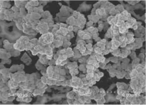
Transition metal oxalates have very often been used as precursors for the preparation of oxides or metals at moderate temperatures. During the oxalate decomposition, nanoparticles are generally formed. They exhibit a high sinterability, or even lower melting points compared with the bulk state. These properties can be used to form solders at low temperatures, with metals having high bulk melting points, or to directly form oxides or metals by local decomposition of the oxalates in a focused laser beam.
Figure 1 : (a) Illustration of the sensitivity of silver oxalate to decomposition: periodic formation of silver particles
under the electron beam of a SEM (b) Formation of Ag nanoparticles inside the oxalate porosity resulting from the thermal decomposition (c) Metallic silver grid obtained by selective laser decomposition of silver oxalate (the remaining oxalate was removed by washing) (d) Copper oxide pattern inside a copper oxalate layer.
This talk details more specifically, the behavior of the silver oxalate and its advantage for the brazing electronic components at low temperature and the shaping of two-dimensional metallic structures, using conventional photolithography machines. Other examples, described and discussed, relate to the production of two-dimensional semiconducing or ferrimagnetic structures based on single or mixed oxides.
Scanning Thermal Microscopy
THERMAL PROBING AND ACTING AT THE NANOSCALE
M. J. Pereira (1), J. S. Amaral (2), N. J. O. Silva (3), V. S. Amaral (4)
(1) CICECO and Physics Department, University of Aveiro, Portugal, [email protected]
(2) CICECO and Physics Department, University of Aveiro, Portugal, [email protected] (3) CICECO and Physics Department, University of Aveiro, Portugal, [email protected]
(4) CICECO and Physics Department, University of Aveiro, Portugal, [email protected] Corresponding author : [email protected]
Keywords : STHM, MICROSCOPY, THERMAL MANAGEMENT, NANO-THERMAL ANALYSIS, ATOMIC FORCE MICROSCOPY (AFM)
Thermal nano-characterization techniques with high spatial resolution are fundamental to address thermal issues which may compromise the performance of miniaturized devices and materials. Scanning thermal microscopy (SThM) is a probing and acting technique based on atomic force microscopy that uses a nano-probe designed to act as a thermometer and a resistive heater. Using a PARK SYSTEMS XE7 Scanning Thermal Microscopy equipment (tip radius ~ 100 nm, temperature up to ~160ºC, sensitivity ~ 0.1ºC and 50 nm spatial resolution) we present the versatility of the technique taking several approaches to study material properties [1]. SThM’s high spatial resolution and ability to perform surface and sub-surface thermal imaging are highlighted in the study of nanocomposite structures with complex inhomogeneities, such as graphene oxide(GO)/poly(lactic acid) (PLA) (Fig. 1). Assisted by the control of the global material’s temperature with external heat sources, the nano-probe’s thermal sensing and actuating abilities induce local structural transformations in materials such as the ferromagnetic shape memory alloy Ni-Mn-Ga and map the spatial distribution of local martensite-austenite transition temperatures.
Fig.1 Left: schematic of the SThM thermal nano-probe heating profile when in contact with the sample; Topography (center) and thermal conductivity contrast (TCC) (right) of GO/PLA nanocomposite (TCC scan showing details on entwining of polymeric chains absent from topography scan). Samples provided by Prof. Ana Barros (Univ. Aveiro) [1] M. J. Pereira, J. S. Amaral, N. J. O. Silva, V. S. Amaral, Microscopy and Microanalysis, V 22, Issue 6 (2016) 1270-1280
Piezoelectric ZnO/PVA composite films
C. Mateo-Mateo (1, 2), J. Yuan (1), M.A. Correa-Duarte (2), A. Colin (1), P. Poulin (1)
(1) Centre de Recherche Paul Pascal (CRPP), CNRS, Université de Bordeaux, France (2)Department of Physical Chemistry, Biomedical Research Center (CINBIO), Universidade de Vigo, Spain
Corresponding author: [email protected]
Keywords : PIEZOELECTRIC, COMPOSITE, FILMS
Piezoelectric energy harvesting[1] is a promising technology for energy recovery from vibration or shock. Although piezoelectric (PZ) materials are used in several applications such as generators, fuel lighters, sensors in automobiles…their use on large scale remains challenging. The main problem relies on the lack of mechanical resistant and efficient materials suitable for new applications.
Herein, we present the hydrothermal synthesis of PZ ZnO nanowires (NWs) with high aspect ratio and the fabrication of ZnO/PVA composite films by embedding the ZnO particles in the polymer matrix. The application of an electrical field allows the alignment of the ZnO NWs giving a strong net macroscopic polarization under stress. Mechanical deformation tests were also performed on the composite films observing the presence of strong voltage peaks that could be related to piezoelectric effects. Other mechanisms related to triboelectric contributions will be discussed.
The combination of the flexible polymer (PVA) with high aspect ratio PZ particles [2] could lead to obtain efficient PZ films with high strength and flexibility.
Fig 1. ZnO/PVA freestanding composite film (A) and SEM images of the composite film (B, C). View of the top Au electrode on the composite film (A). Electrical response when the film is mechanically deformed (D).
REFERENCES
[1] J. Curie, P. Curie, Bulletin de la Société minéralogique de France, vol 3 (1880) 90-93
When high pressure-high temperature
synthesis helps to discover new oxides:
EXAMPLES FROM MULTIFERROISM AND MAGNETIC
FRUSTRATION
P. Zuo (1,2), C. Darie (1,2), C. Goujon (1,2), M. Legendre (1,2), C.V. Colin (1,2), H. Klein (1,2), P. Bordet (1,2)
(1) Univ. Grenoble Alpes, Inst NEEL, F-38000 Grenoble, France (2) CNRS, Inst NEEL, F-38000 Grenoble,
Corresponding author : [email protected]
Keywords : HIGH PRESSURE- HIGH TEMPERATURE, OXIDES, MULTIFERROISM, MAGNETIC FRUSTRATION
In the last decades, high pressure (> 1GPa) has been increasingly used in different fields of research ranging from earth science to solid state physics, chemistry and material science. At Institut Néel, Grenoble, a state-of-the-art and unique instrumental park is dedicated to solid-state synthesis, crystal growth and characterization of materials under extreme conditions (Fig.1).
In this contribution we start with a description of these high pressure (up to 15GPa) and high temperature (up to 1500°C) facilities, with an extension to recent developments and new experimental set-up as DTA (Differential Thermal Analysis) and XRD (X-Ray Diffraction).
In a second part, we will present two studies of HP-HT syntheses in the field of research of new materials that are multiferroic or show magnetic frustration, respectively. The case of a new form of a spin liquid phase1 Ba
3NiSb2O9
obtained under high pressure-high temperature will be presented. The second example will show the stabilization of small rare-earth compounds in the series NaLnCoWO6 (Ln = rare earth), a new class of potentially multiferroic
compounds, with the help of HP-HT2.
Fig. 1: Belt (left) and Conac (right) devices at Institut Néel
(1) “A new high pressure form of Ba3NiSb2O9” C. Darie, C. Lepoittevin, H. Klein, S. Kodjikian, P. Bordet, C.V. Colin, O.I.Lebedev, C. Deudon, C.
Payen Journal of Solid State Chemistry 237(2016)166–173
(2) "Structural Study of A Doubly Ordered Perovskite Family NaLnCoWO6 (Ln=Y, La, Nd, Pr, Sm, Eu, Gd, Tb, Dy, Ho, Er, Yb): Hybrid Improper
Ferroelectricity in Nine New Members" P. Zuo, C. V. Colin, H. Klein, P. Bordet, E. Suard , E. Elkaim and C. Darie submitted to Inorganic Chemistry
Diamond interfaces in power devices:
Electron microscopy issues
D. Araújo (1), J.C. Piñero(1), F. Lloret(1,2), P. Villar(1), M. Gutiérrez (1), M.
Florentin (2), T. Pham (2), D. Eon(2), J. Pernot (2)
(1) Departamento de ciencias de los materiales IM y QI, Universidad de Cádiz, 11510 Puerto Real (Cádiz), Spain, [email protected]
(2) Institut Néel, CNRS-UJF, av. Des Martyrs, 38024 Grenoble (France) (3) Univ. Grenoble Alpes, F-38000 Grenoble (France)
(4) Institut Universitaire de France, 103 Boulevard Saint Michel, 75005 Paris (France)
Corresponding author : [email protected]
Keywords : DIAMOND, POWER DEVICES, ELECTRON MICROSCOPY, MPCVD, TEM
The growing interest on the applications of diamond for power devices relies in its promising properties as a high breakdown field, high carrier mobility and high thermal conductivity. Indeed, diamond-based Schottky diodes, using Zr metal over oxygen-terminated diamond surfaces, showing power figure of merit of 244 MWcm-2 have been
recently reported. However, designing reliable diamond Schottky diodes (SBD) or diamond-MOS capacitors are still a technological challenge. Indeed, a lack of knowledge of the bandgap behavior in hydrogen/oxygen-terminated diamond surfaces contacting metal and oxide layers should be first understood to take advantage of the outstanding properties of diamond in the electronic power devices engineering.
To pursue this objective, Scanning Transmission Microscopy (STEM)-based techniques as High Angle Annular Dark Field (HAADF) and Electron Energy Loss Spectroscopy (EELS), joined with X-ray photoelectron spectroscopy (XPS) and cathodoluminescence (CL), are used to analyse the diamond/oxide interfaces of MOSFETs and SBD structures.
The atomic surface configuration related to diamond/Al2O3 interface bandgap levels joined to the ALD-grown oxide
bandgap itself are reported. The effect of the Cherenkov and plasmon-related peaks on the Eg determination will be
evaluated.
A relationship between nanostructure and energy bandgap in oxide layer at a nanometer-scale will be presented showing the importance of such aspects in the design of either MOSFET or SBD diamond related devices.
Electrodeposition strategies for
antibacterial calcium phosphate
coatings on titanium
C. Pierre (1), E. Vidal (2), G. Bertrand (1), E. Ruperez (2), C. Rey (1), D. Rodriguez (2), C. Combes (1)
(1) CIRIMAT, Université de Toulouse, France, [email protected] (2) Biomaterials, Biomechanics and Tissue Engineering Group, UPC, Spain,
Corresponding author: [email protected]
Keywords: ELECTRODEPOSITION, CALCIUM PHOSPHATE, ANTIBACTERIAL, COATING, TITANIUM IMPLANTS
Titanium and its alloys are the most used biomaterials for orthopedic and dental implants thanks to their good biocompatibility. Nevertheless, osseointegration of these implants is long to achieve and that is why surface treatments are applied to promote bone healing and growth. For that purpose, calcium phosphate coatings are commonly prepared [1]. Several coating processes can be used such as plasma spray, sol-gel, laser-deposition or electrodeposition. Among these techniques, electrodeposition is very attractive because it allows to produce thin coating on complex shapes and it is a low temperature process that permits to associate temperature-sensitive molecules of biological and/or therapeutic interest [2]. A second problem linked to the implantation is the bacterial colonization that may lead to implant loosening. The purpose of this study is to create a low temperature calcium phosphate bioactive coating on titanium to enhance osseointegration and also to associate an antibacterial agent with this layer to prevent post-operative infections [3], [4]. In this study, two strategies have been developed:
(5) Calcium phosphate electrodeposition was realized at constant potential and an antibacterial element (ie. Ag, Cu,…) is then introduced by ionic exchange;
(6) Calcium phosphate and an antibiotic molecule were co-deposited by pulsed-electrodeposition.
The influence of the process parameters (current density/potential, ton/toff ratios and electrolyte temperature) has
been investigated. Scanning electron microscopy, X-ray diffraction, Raman and FTIR spectroscopies were used to characterize the coatings with and without the antibacterial agent. Moreover, adhesion between the substrate and the coating was also investigated. Preliminary antibacterial and drug release tests were also realized.
Coatings prepared by the two different methods were composed of mixed calcium phosphate phases. Changes in the process parameters produced different crystal morphologies. The addition of an antibacterial compound did not seem to influence the coating formation and its chemistry. All the studied coatings had good mechanical stability, in terms of adhesion and shear strength. In vitro antibacterial properties were also demonstrated against E. Coli and
S. Aureus.
[1] R.A. Surmenev et al., Acta Biomater., vol. 10, no2, pp 557-579, 2014 [2] R.I. Asri et al., J. Mech. Behav. Biomed. Mater., vol. 57, pp 95-108, 2016 [3] D. Scharnweber et al., J. Mater. Med., vol. 18, no2, pp 391-397, 2007 [4] X. Lu et al., J.R. Soc. Interface, vol.8, no 57, pp 529-539, 2011
Acknowledgments: The authors thank the Midi-Pyrénées Region (BIOACTISURF project n°14054394), MAT2015-67183-R(MINECO/FEDER), AGAUR FI-DRG and the Cost Action TD1305 for supporting this research work.
Aberration-Corrected Electron Microscopy
of Advanced Functional Nanomaterials
C. Magén (1)
(1) Laboratorio de Microscopías Avanzadas (LMA), Instituto de Nanociencia de Aragón (INA) - ARAID, Universidad de Zaragoza, Spain, [email protected]
Corresponding author : [email protected]
Keywords : (SCANNING) TRANSMISSION ELECTRON MICROSCOPY, ABERRATION CORRECTION, NANOMAGNETISM, COMPLEX OXIDES, NANOSTRUCTURES
The fast emergence of Nanoscience during the last decades has been favoured by the development of new nanocharacterization tools with unprecedented resolution and sensitivity. In addition to the invention of scanning probe microscopy, traditionally considered the starting signal of Nanotechnology, the development of other types of microscopy techniques have contributed decisively to our understanding of the world at nanometer scale. In the field of Transmission Electron Microscopy (TEM), the most crucial milestone has been the development of aberration correctors. This new technology has offered scientist the possibility of atomically resolved characterization of structural, chemical and electronic properties of a wide range of advanced (nano)materials, with an undeniable impact on the development of novel materials in fields such as oxide thin films, semiconductor nanostructures, carbon based materials, magnetic nanostructures, nanoparticles, etc.
This lecture will review several applications of advanced TEM techniques that have been developed in the last years at the LMA, focusing on the work carried out in advanced materials for spintronic applications and the infrastructures available at the LMA to carry out these investigations. One of the subjects will the characterization of multiferroic oxide thin films, particularly the analysis of defects and domain walls that confer these materials unexpected physical properties, by the combination of atomic resolution imaging and spectroscopic techniques. Secondly, the potential of interferometric TEM techniques for the imaging of magnetization states at the nanometer scale will be demonstrated by illustrating the characterization of individual magnetic nanostructures and heterostructures grown by focused electron and ion beam techniques with different architectures.
Flexoelectricity: from semiconductors to
memory devices
G. Catalan (1, 2), J. Narvaez (2, 3), K. Cordero (2), U. Bhaskar (2,4), N. Domingo (2)
(1) ICREA, Barcelona, Spain
(2) ICN2 (Institut Catala de Nanociencia i Nanotecnologia), Barcelona, Spain (3) Universidad de los Andes, Bogotá, Colombia
(4) Purdue University, Indiana, USA
Corresponding author: [email protected]
Keywords : FLEXOELECTRICITY, FERROELECTRICITY, PIEZOELECTRICITY, MEMS, OXIDES
Flexoelectricity allows inducing polarization by bending (or by any other inhomogeneous deformation) in dielectrics of any symmetry, including centrosymmetric materials such as SrTiO3 and also ferroelectrics such as BaTiO3. While
this has been traditionally exploited for making piezoelectric-like sensors using non-piezoelectric materials, there is a much wider variety of functional possibilities that have only recently started being explored. In my talk, I will cover three of them which our laboratory has been very directly involved:
1) Measuring flexoelectricity not on dielectric insulators but on semiconductors. In the latter, we have seen that the effective flexoelectric coefficient can be orders of magnitude larger than the flexoelectricity of insulators, and in addition it scales with thickness in such a way that it is a relevant effect even at the macroscale.
2) Using inverse flexoelectricity to make actuators that bend in response to a voltage (as opposed to sensors that generate a voltage in response to bending). These have been made in the form of MEMS cantilevers grown on silicon substrates, and are thus a technologically promising device concept.
3) Exploiting flexoelectricity not only to mechanically write ferroelectric domains, but also to mechanically read them, enabling the full voltage-free operation of a ferroelectric memory.
Characterizing magneto-thermal
materials and processes at CICECO-UA
INFRASTRUCTURES AND EXPERTISE
V. S Amaral (1), J. S. Amaral (2), N. J. O. Silva (3), A. Davarparnah (4), F. Mohseni (5), T. Santos (6), M. J. Pereira (7)
CICECO and Physics Department, University of Aveiro, Portugal (1) [email protected] ; (2) [email protected] ; (3) [email protected] ; (4) [email protected] ; (5) [email protected] ;
(6) [email protected] ; (7) [email protected] Corresponding author : [email protected]
Keywords : MAGNETOMETRY; THERMAL CONDUCTIVITY; INFRARED THERMOMETRY; MAGNETOCALORIC
Magnetic materials are in the front line to face challenges of energy conversion, savings and harvesting. The application of magnetocaloric materials into systems working in the vicinity of phase transitions provide the gains necessary to develop sustainable strategies for their innovative use. In the frame of thermal systems, mostly significant for cooling/heating, electrical energy supply processes and heat induction, materials optimization must also comprise their thermal conductivity, dynamic behavior and its dependence on the magnetic state of materials. To face such a combined study towards optimization of magneto-thermal materials and processes, our group at CICECO-Aveiro Institute of Materials developed a new research infrastructure. Its main instruments are:
Quantum Design MPMS3 SQUID-VSM Magnetometer (7 Tesla/ 1.8K-400K)
HOT Disk TPS 2500 Thermal Properties Measurement system (thermal conductivity and specific heat) Transient Plane Source Method, (0.005 to 1800 W/m/K.) for solids or liquids, with bath (-20ºC to 180ºC) and oven (up to 750ºC). A custom assembly for measurements under 1 Tesla magnetic field was also built.
FLIR 5600 infrared thermography camera ( -20 up to 3000ºC and 20mK resolution, up to 200 Hz frame rate in full resolution). Additional microscope (X5 lens, micrometer resolution) for local thermal mapping. A custom assembly for measurements under magnetic field cycling up to 1 Tesla was built.
PARK XE-7 Atomic Force Microscope (AFM) with Scanning Thermal Probe Microscopy (SThM) probe and actuator (better than 100 nm resolution, with tip temperature up to 160ºC).
We present highlights in the context of developing materials, heat transfer, and measurement techniques.
CICECO-Aveiro Institute of Materials, POCI-01-0145-FEDER-007679 (FCT Ref. UID/CTM/50011/2013) is financed by national funds through FCT/MEC(PIDDAC) and co-financed by FEDER under the PT2020 Partnership Agreement.
Photonic Crystals and Related
Nanostructures for the Control of Light
Trapping and Emission
C. Seassal, L. Lalouat, N.-V. Hoang, H. Ding, H.S. Nguyen, E. Drouard
Université de Lyon; Institut des Nanotechnologies de Lyon-INL, UMR CNRS 5270, CNRS, Ecole Centrale de Lyon, Ecully F-69134, France
Corresponding author : [email protected]
Keywords : NANOPHOTONICS, PHOTONIC CRYSTALS, LIGHT TRAPPING, WAVELENGTH CONVERSION, LIGHT EMISSION
Photonic crystals and related structures offer great potentialities for the next generation photovoltaic solar cells, light emitters and wavelength converters. In this communication, we will present advanced designs and strategies to carefully control light-matter interaction with advanced photonic nanostructures. Such control is based on photonic crystals and metastructures including active media and enabling a tight control of dispersion characteristics [1-2]. We will also discuss on the compromise between perfectly ordered and perturbated nanopatterns [3-4].
Theoretical predictions and experimental results will be presented as illustrations. We will discuss on the integration of photonic nanopatterns in thin film silicon solar cells, with a view to optimize their conversion efficiency. We will also present approaches and results related to light-emitting and wavelength conversion photonic structures using various types of active media.
[1] J. Marques-Hueso, R. Peretti, R. Abargues, B. S. Richards, C. Seassal, J. P. Martínez-Pastor, “Photonic Crystal-Driven Spectral Concentration for Upconversion Photovoltaics,” Advanced Optical Materials 3, pp568-574 (2014) [2] R. Peretti, G. Gomard, L. Lalouat, C. Seassal, E. Drouard, “Absorption control in pseudodisordered photonic-crystal thin films,” Phys. Rev. A 88, 053835 (2013)
[3] C. Seassal, L. Lalouat, H. Ding, E. Drouard, “Carefully mixing disorder and periodicity to optimize solar light trapping”, SPIE Newsroom, Solar & Alternative Energy, 14 July 2016
[4] L. Lalouat, H. Ding, B. Gonzalez-Acevedo, A. Harouri, R. Orobtchouk, V. Depauw, E. Drouard, C. Seassal, “Pseudo-disordered structures for light trapping improvement in mono-crystalline Si thin-films”, Solar Energy Materials & Solar Cells, 159, 649-656 (2016)
P3MT/VACNT/Al Nanocomposites
Electrodes With High Capacitance For
Supercapacitor
T. Vignal,a,b L. Darchy,b A. Boisset,b H. Hauf,b J. Descarpentries,b Q.
Mestre,c M. Pinault,c M. Mayne-L’Hermite,c P. Banet,a P.H. Auberta
a LPPI, EA 2528, 5 MAIL Gay Lussac, Université de Cergy-Pontoise, France b NAWATechnologies SA, 190 avenue Célestin Coq-ZI, ROUSSET, France
c NIMBE, CEA, CNRS, Université Paris-Saclay, CEA Saclay, Gif-sur-Yvette, France
Corresponding author: [email protected]
Keywords : POLY(3-METHYLTHIOPHENE), CARBON NANOTUBES, ELECTRODE MATERIALS, SUPERCAPACITORS
Supercapacitors are desirable for applications requiring high power densities. Among the various types of supercapacitors, electrochemical ones based on electronically conducting polymers (ECP) as electrode material are particularly interesting because of their high capacitance (1). However, their energy densities and their electrochemical stability are still limited (2,3). In order to improve the capacitance and the energy density of such pseudo-capacitive supercapacitors, our strategy consists in making nanocomposite electrodes of poly-3-methylthiophene (P3MT) in ionic liquid media. These depositions were made on the surface of nanostructured electrodes composed of very dense carpet of vertically aligned carbon nanotubes (1011 – 1012
CNT/cm²) on an aluminium collector (VACNT/Al). In this study, different electropolymerizations methods (cyclic voltammetry, galvanostatic, potentiostatic, pulsed methods (3,4)) were used to optimized the deposition and the storage properties of P3MT. Thus, nanocomposites with weight ratios of P3MT/(P3MT+CNT) ranging from 5 to 90% were obtained and characterized by electrochemistry (CV and EIS) and microscopy. The results show that conformal depositions of polymers were obtained. In the case of the best nanocomposites, the electrodes capacitance increase from 32 mF/cm² to 1300 mF/cm². Finally, stability tests of electrodes and coin cells assembly were studied and their performances will be presented.
References:
[1] Mastragostino M. et al., Adv. Mater. 1996, 8, 331. [2] Schnoor T. I.W. et al., Carbon 2013, 60, 229.
[3] Lagoutte S. et al., Electrochimica Acta 2014, 130, 754. [4] Sharma R.K. et al., Electrochem. Commun. 2008, 10, 268.
Biomimetic nanopore to design “smart”
membranes
S. Balme (1)
(1) Institut Européen des Membranes, Université de Montpellier, France, Corresponding author : [email protected]
Keywords : SINGLE NANOPORE, MEMBRANE, BIOMIMETIC, SENSOR, SOFT MATTER
In the life science, it is well known that ionic bio-channels insure exchange and communication of living cells. Their properties in terms of ionic permeability, selectivity and response regarding the environment are exceptional. Unfortunately, the transfer of these properties to artificial set-up whose the mechanical strength is high enough to be useful in many different types of applications has not been made. The limitations of artificial nanopore membranes prepared by track-etched polymer sheets or transmission electron microscopy irradiation of thin silicon nitride film are the weak ionic selectivity and unresponsiveness against stimuli. Thus the main challenge consists of mimicking biological channels properties to design artificial nanopore membrane which is able to modulate their transport. To achieve this goal two strategies will be explored. The first one consists to a solid-state nanopore functionalized with more and less complex systems which permits to improve their properties. The second strategy is based in insertion of protein inside nanopore in order to obtain hybrid biological/artificial system. This strategy aims to combine the advantages of both solid-state nanopores (robustness, number, size and shape control) and biological channels (selectivity, precise structure)
In this talk, we will discuss on the different strategies to functionalize single track-etched nanopore using chemical grafting of (bio)macromolecule, self-assembly of poly-electrolytes or direction insertion of ion channel. Such functionalization permits to obtain nanopore with high ionic selectivity such as ionic-diode as well as design nanovalves which respond to ligand anchoring, pH, light. We will show also the potentialities of functionalized nanopores for specific bio-sensor as well as osmotic energy.
FE-AFE based functional oxide materials
F. Ponchel(1), D. Rémiens(1), T. Lasri(2), X. Guo(1, 3), L. Jianyun(1, 3), H.
Liuyang(1, 3), J. Ge(1, 3), Y. Chen(3), G. Wang(3)
(1) IEMN – UVHC – UMR CNRS 8520 – Groupe MAMINA – Le Mont Houy 59313, Valenciennes Cedex 9, France
(2) IEMN – DHS – UMR CNRS 8520 – Groupe MITEC - Cité scientifique
Avenue Henri Poincaré, CS 60069 - 59652 Villeneuve d'Ascq Cedex, France [email protected]
(3) Key laboratory of Inorganic Functional Materials and Devices
Shanghai Institute of Ceramics, Chinese Academy of Sciences (SICCAS) 1295 Dingxi Road, Shanghai, 200050, China
Corresponding author : [email protected]
Keywords : ANTI FERROELECTRIC, STORAGE ENERGY, HIGH FREQUENCY TUNABILITY. LEAD FREE PIEZOELECTRIC MATERIAL
In this talk we will present some results obtained in three directions, namely anti ferroelectric (AFE) thin films for energy storage applications, ferroelectric thin films for microwave applications and lead-free ferroelectric thin films which applications are potentially very large. Anti Ferro Electric (AFE) thin films for energy storage applications. The well known PbZrO3 (PZ) AFE material is deposited by rf magnetron sputtering on silicon substrate. More precisely, highly (001)-oriented pure PZ films and Sn-substituted PZ films are deposited on (001)-LaNiO3 buffered SiO2/Si substrates. Different Sn-substituted PbZrO3 films (PbZr1-xSnxO3, x = 0%, 3%, 5%, 10%) with orthorhombic anti-ferroelectric phase are fabricated. The effects of Sn substitution on the structure and energy performance have been investigated in details. In another topic research, the dielectric properties (relative permittivity and losses) of PZT, PST and BST films were measured up to 60 GHz using coplanar waveguides (CPW). Based on the CPW scattering parameters measurement, the frequency dependence of the complex permittivity has been determined thanks to a homemade numerical code based on finite elements. Even at 60 GHz a large tunability of 47%, 30% and 60% has been measured for PZT, PST and BST respectively. Lead-based piezoelectric materials are well known for their excellent piezoelectric properties. However, due to the effects of lead toxicity, since recently it is desired to reduce lead-based materials usage in electronic devices. Therefore, lead-free materials have gained much interest in the microelectronic industry. In this context we have been working on Lead-free Bi0.5Na0.5TiO3 (BNT) piezoelectric thin films. BNT films were deposited on Pt/TiOx/SiO2/Si substrates by sputtering. a piezoelectric coefficient (d33effmax) of 80 pm/V was obtained. BNT is regarded as an interesting alternative to PZT for MEMS application.
Energy Harvesting Materials Based on
Carbon Nanotube Fibre for Tough
Electronics
A. Monreal-Bernal, Juan J. Vilatela
IMDEA Materials Institute, Eric Kandel 2, Getafe 28906, Spain
Corresponding author : [email protected]
Keywords : CARBON NANOTUBE FIBRE, ZINC OXIDE, TOUGH ELECTRONICS, SCHOTTKY BARRIER, PHOTOCONDUCTIVITY
Nanocarbons are very popular materials to interface with semiconductors. They combine extraordinary mechanical properties, high thermal stability, thermal conductivity and more importantly, very high carrier mobility. They have been shown to improve performance of (opto)electronic devices including solar cells, photoelectrochemical cells, and other applications involving interfacial charge transfer processes. A porous network of CNTs can act as a large-area scaffold for the semiconductor and be used as current collector to harvest carriers generated in the semiconductor by photovoltaic, photochemical and piezoelectric processes.
In the quest for making robust, flexible large-area devices based on nanocarbon/semiconductor hybrids (and other semiconductors) challenges remain in terms of the quality of nanocarbon/semiconductor junction that can be produced using simple large-area processes, and the mechanical robustness of these hybrid materials.
In this work we present a study on the structure and electronic properties of 10 cm2 scale ZnO/CNT fiber
materials. The carbon nanotube fibers (CNTf) combine a high surface area with bulk tensile strength, toughness and in-plane conductivities superior to steel and much greater than those of conventional vacuum-filtered CNT/graphene membranes. They are therefore ideal electrodes/current collectors to be combined with semiconductors, not only to produce new tough and efficient devices, but also as a test system to study low-dimensional properties of CNT/semiconductor junctions on a macroscopic scale. With these objectives in mind, this work presents a detailed characterisation of the electronic properties of bulk Schottky barrier heterojunctions between CNTf and ZnO, from which various parameters of interest are extracted, including junction energy levels, dopant concentration, ideality factor and interfacial resistance. The hybrid material is also shown to be highly piezoresistive and piezoelectric, and as a demonstration of interfacial charge transfer we show piezoelectric energy harvesting.
Epitaxial growth of nanostructured
functional oxide thin-films by solution
chemistry
José M. Vila-Fungueiriño (1), A. Gómez (2), R. Moalla (3), G. Saint-Girons (3), C. Magén (4), J. Gázquez (2), R. Bachelet (3), M. Gich (2), F. Rivadulla (5), A. Carretero-Genevrier (1)
(1) Institut d’Électronique et des Systèmes (IES), UMR 5214, Bâtiment 5, 860 rue Saint Priest, 34090 Montpellier, France
(2) Institut de Ciència de Materials de Barcelona (ICMAB), Consejo Superior de Investigaciones Científicas (CSIC), Campus UAB 08193 Bellaterra, Spain
(3) Institut des Nanotechnologies de Lyon (INL) UMR 5270, 36 avenue Guy de Collongue, 69134 Ecully, France
(4) Departamento de Física de la Materia Condensada, Universidad de Zaragoza, Zaragoza, Spain
(5) Centro de Investigación en Química Biolóxica e Materiais Moleculares (CIQUS), Universidade de Santiago de Compostela, 15782 Santiago de Compostela, Spain [email protected]
Keywords: EPITAXIAL THIN FILMS, OXIDES, POLYLER ASSISTED DEPOSITION
The variety of structures and properties provided by oxides offers an important route for the development of new devices integrated on different substrates such as silicon. At the interface of thin films and nanostructures the physical properties can strongly differ from bulk state due to the low dimensionality conditions imposed. In this regard, the control of crystallization mechanism at the nanoscale provided by the chemical solution methods is an affordable alternative to physical deposition techniques. However, the integration of functional oxides on silicon need to be further developed due to the dissimilarities on these materials, i.e. chemical reactivity, structural parameters, and thermal stability.
This work describes the synthesis of high quality epitaxial thin films and heterostructures of different functional oxides by Chemical Solution Deposition (CSD). In combination with Molecular Beam Epitaxy (MBE) these oxides can be epitaxially integrated in Silicon. In particular, complex oxide such as perovskites nanostructured thin films are synthetized by using a CSD method called Polymer Assisted Deposition (PAD) [1,2] supported with the controlled epitaxial growth of SrTiO3 (STO) buffer layer on Si [3]. By this route, La0.7Sr0.3MnO3 (LSMO) ultrathin films
with abrupt interfaces and nanopillared BaTiO3 (BTO) on LSMO with good functionalities can be obtained exhibiting
a great technological potential. The complementary of physical and chemical deposition techniques may stablish the basis for the development of low cost functional devices compatible with standard microfabrication technologies.
[1] Q. X. Jia et al. Nature Materials 3, 529 (2004).
[2] J. M. Vila-Fungueiriño et al. ACS Appl. Mat. Interfaces 7, 5410 (2015). [3] J. M. Vila-Fungueiriño et al. Front. Phys. 3, 38 (2015)
Confinement of organic dyes inside
carbon nanotubes
A. Salvati(1), A. Belhboub(1), Alvarez (1), R. Leparc (1), S. Rols (6),P. Hermet(1),B. Jousselme(3), K. Suenaga (4), A. Rahmani (5) J-L.
Bantignies (1)
(1) Laboratoire Charles Coulomb, University of Montpellier, France, (2) Institut Laue-Langevin, Grenoble, France,
(3) Laboratoire d’Innovation en Chimie des Surfaces et Nanosciences (LICSEN), CEA Saclay, France
(4) Nanomaterials Research Institute, AIST, Tsukuba, Japan
(5) Laboratoire d’Etude des Matériaux Avancés et Applications,Université Moulay Ismaïl, Morocco (6) Institut Charles Gerhardt Montpellier,, University of Montpellier, France
Jean-Louis Bantignies : [email protected] Keywords : ENCAPSULATION, CONFINEMENT, NANOTUBE, VIBRATIONAL SPECTROCOPIES, DFT
Opto-electronic properties of single-walled carbon nanotubes can be significantly modified by chromophore confinement into their hollow core. This presentation deals with quaterthiophene derivatives encapsulated into nanotubes displaying different diameter distributions. We show that the supramolecular organizations of the confined chromophores depend on the nanocontainer size. The Raman radial breathing mode frequency is monitored by both the number of confined molecules into a nanotube section and the competition between dye/dye and dye/tube wall interactions. The confinement properties lead also to an exaltation of the infrared absorption
response1 in single-walled carbon nanotubes from dye molecule interactions due to a symmetry breaking, allowing
us, thanks to the complementarity of DFT calculations and experimental IR investigations to study interactions between both subsystems. Significant electron transfer from the confined molecules to the nanotubes is also reported from Raman investigations. This charge transfer leads to an important enhancement of the photoluminescence intensity by a factor of nearly five depending on the tube diameter. In addition, close to the molecule resonance, the magnitude of the Raman G-band shifts is modified and the intensity loss is amplified, indicating a photo-induced electron transfer. Results are discussed in the frame of electron-phonon coupling. Thus, confinement species into nanotubes allow moving the Fermi level and consequently to monitor their opto-electronic properties.
Reference