HAL Id: tel-00453410
https://tel.archives-ouvertes.fr/tel-00453410
Submitted on 4 Feb 2010
HAL is a multi-disciplinary open access
archive for the deposit and dissemination of sci-entific research documents, whether they are pub-lished or not. The documents may come from teaching and research institutions in France or abroad, or from public or private research centers.
L’archive ouverte pluridisciplinaire HAL, est destinée au dépôt et à la diffusion de documents scientifiques de niveau recherche, publiés ou non, émanant des établissements d’enseignement et de recherche français ou étrangers, des laboratoires publics ou privés.
Superconducting-magnetoresistive sensor: Reaching the
femtotesla at 77 K
Myriam Pannetier-Lecoeur
To cite this version:
Myriam Pannetier-Lecoeur. Superconducting-magnetoresistive sensor: Reaching the femtotesla at 77 K. Condensed Matter [cond-mat]. Université Pierre et Marie Curie - Paris VI, 2010. �tel-00453410�
1
Habilitation à Diriger des Recherches
Présentée par
Myriam Pannetier-Lecoeur
Service de Physique de l’Etat Condensé – CEA Saclay
Superconducting-magnetoresistive sensor:
Reaching the femtotesla at 77 K
Soutenue le 28 Janvier 2010 devant le jury composé de :
- Claire Baraduc, SPINTEC-CEA-Grenoble ; France (rapporteur)
- Claude Chappert, Institut d’Electronique Fondamentale, Orsay ; France
(rapporteur)
- John Michael David Coey, Physics Department, Trinity College Dublin ; Ireland
(examinateur)
- Claude Fermon, SPEC-CEA-Saclay ; France
- Risto Ilmoniemi, BECS, Aalto University Helsinki ; Finland (rapporteur)
- Jérôme Lesueur, ESPCI-UPMC, Paris ; France (examinateur)
2
Contents
Introduction ... 5
Magnetic sensors ... 6
Sensing the magnetic field ... 6
Sensitive and highly sensitive magnetometry ... 7
Field sensors: ... 7
Hall effect sensors ... 7
AMR and GMR sensors ... 8
Flux sensors: ... 8
Coils ... 8
Fluxgates ... 8
SQUIDs ... 9
Spin electronics for field and current sensing ... 10
Proposal for a new type of sensor ... 12
Mixed sensor: principle, fabrication, characteristics ... 13
Principle ... 13
Superconducting flux transformer ... 13
Magnetoresistive element ... 16
GMR composition ... 16
GMR sensor design ... 17
Mixed sensor noise evaluation ... 19
Fabrication ... 20
Low-Tc mixed sensor: ... 20
High-Tc mixed sensor: ... 21
Characteristics ... 22
Measuring the gain of the sensor ... 22
Measuring the noise of the sensor ... 24
Mixed sensors for low frequency measurements ... 27
Low frequency response; sensitivity ... 27
3
Biomagnetic signal detection ... 30
Biomagnetic signals ... 30
Cardiac signals: ... 30
Neuronal signals: ... 31
First biomagnetic measurements with a mixed sensor ... 32
Recording (also) the artifacts and ballistocardiography ... 34
Discussion on biomagnetic measurements with a mixed sensor ... 35
1/f reduction techniques ... 35
Saturating the supercurrent ... 36
Local heating technique ... 36
Conclusion ... 38
Mixed sensors for resonant signals detection ... 39
Sensitivity to radiofrequency signals ... 39
Detection of a resonant signal ... 40
Nuclear Magnetic Resonance experiment ... 40
Low field NMR and MRI ... 42
Mixed sensors and resonant signal detection ... 43
Nuclear Quadrupolar Resonance and explosives detection ... 45
Nuclear Quadrupolar Resonance ... 45
Experimental setup... 46
Detection of explosives ... 47
Very low field Nuclear Magnetic Resonance and Imaging ... 49
Experimental set up ... 49
Sequences and NMR signals ... 50
Discussion and perspectives on low-field MRI ... 51
Perspectives ... 55
Achieving subfemtotesla sensitivity ... 55
Design and fabrication ... 55
Materials ... 56
Tunnel Magneto Resistive (TMR) mixed sensors ... 57
All oxide mixed sensors ... 57
Realizing combined biomagnetic signal measurements and MRI ... 58
References ... 60
4
5
Introduction
My research activities have been first focused on high-Tc superconductivity (PhD and first
post-doctoral fellowship). During my PhD thesis, I have studied Abrikosov vortex dynamics in type II superconducting structures through transport measurements. During my post doctoral stay in Amsterdam I had investigated the flux penetration in bulk and thin films superconductors with the aim of magneto-optical imaging.
Since I arrived at the Service de Physique de l’Etat Condensé at CEA Saclay, end of 2001, I have been involved in understanding of transport and noise mechanisms in nanoscale magnetic structures and in spin electronics systems, such as spin valve Giant Magneto-Resistances (GMR) and Tunnel Magneto-Magneto-Resistances (TMR). Exploring the underlying phenomena, especially in the low frequency noise, led me to develop magnetic field and current sensing devices with improved performances. Part of the sensor development is related to room temperature applications, dedicated to industrial needs (2D compass, voltage monitoring in fuel cells…), magnetic imaging system (non destructive evaluation, magnetic mapping for Earth field sciences) and also for magnetic biochips.
In order to measure extremely weak fields, in particular those produced during the cognitive tasks by neuronal activity, we have proposed and realized femtotesla sensors (or mixed sensors) based on the association of spin electronics and superconductivity, which offer an alternative in thin film technology to the most sensitive existing devices, the low Tc SQUIDs
(Superconducting Quantum Interference Devices).
In this report, I present in the first part the state of the art and requirements for magnetic field measurements in the low value range (lower than 1 µT), then I detail the principle, realization and characteristics of the mixed sensors.
Amongst the weakest magnetic signal of interest are those produced by the body, in particular the heart and brain electrical activity, and the resonant signal of nuclei excited through Nuclear Quadrupolar Resonance (NQR) and Nuclear Magnetic Resonance (NMR) experiments. I show in the third part how we succeed in using mixed sensors to detect the magnetic heart signal. Resonant experiments have been also successfully carried to perform solid explosives detection by NQR, and proton NMR, opening way to low-field MRI, as detailed in the fourth part of this report.
6
Magnetic sensors
Sensing the magnetic field
For more than four thousand years, men have developed instruments to probe one of the most mysterious and fascinating phenomenon, the magnetic field. First by building up compasses to indicate the direction of the Earth field, then later exploiting some properties of materials, like Hall effect or induced current (Ampere law) to measure the strength of the field. From the discovery of electrical current and of the link between current and field in the XIXth century, needs of accurate sensors to measure both field and current had led to many devices. Most of them are still widely used in many applications, from current sensing in cars or electricity meters, to navigation systems in aircraft or spatial probes.
As the magnetic field can exhibit a wide range of amplitudes and frequencies, a large variety of sensors is needed to probe it in the correct range.
Figure 1 illustrates the 15 orders of magnitude in magnetic field one may find in our environment and four kinds of magnetic sensors based on different physical effect that might be used, depending on the strength of the signal.
Figure 1 : Scale of quasi-static magnetic field generated in our environment compared to the range of sensitivity of few commonly used magnetic sensors.
One may classify the magnetic sensors by their detectivity, which is their ability to detect a certain level of signal (in tesla) over their intrinsic noise [1] .
7
Here I will focus on the most sensitive sensors, those addressing signal much lower than the Earth magnetic field, ultimately like those emitted by the electrical currents circulating in the body (heart, neurons, nerves…) whose strength ranges from picoteslas (10-12T) to femtoteslas (10-15T).
Sensitive and highly sensitive magnetometry
A proper sensor will be defined by the signal which is targeted. First characteristic, but not the sole, is the amplitude of this signal in tesla (or A/m). Another very crucial aspect is the source size and its distance. A small sensor may not be appropriate for a distant source. On contrary, a very sensitive sensor integrating the signal over a large surface might not be fitted to a very local source. The environment is also a key parameter for the choice of the sensor. Environmental conditions (noise, temperature range, vibrations…) and dynamics are also important parameters to be taken into account.
Below the microtesla, four technologies can be depicted for field sensing, each of them presenting advantages and drawbacks. The first two technologies (Hall and MR sensors) are sensing the magnetic field, whereas the last three (coils, fluxgates and SQUIDs) are sensing the magnetic flux over a surface. This distinction will be important also in the applications.
Field sensors:
Hall effect sensors
The first technology and oldest known is based on the Hall effect. Discovered by Edwin Herbert Hall in 1879, it is described as the appearance of transverse voltage in a conductor biased with a current and over which a perpendicular field is applied. The motion of charge carrier deflected by the magnetic field is responsible of this voltage which is directly proportional to the applied field (see Figure 2).
Figure 2 : Hall effect principle.
A Hall effect sensor is a linear absolute sensor and its sensitivity can be below the microtesla. These sensors are rather cheap and can be reduced to micron-sized with the help of semiconducting material and 2D-electron gas (Hall microprobes). They probe the out of plane component of the field.
8 AMR and GMR sensors
Second technology is using the magnetoresistive effect. First discovered, the anisotropic magnetoresistance is the property of some metals to see their resistance changing in the presence of an applied field (parallel to the plane). This effect is rather small (less than 3% in 1 mT) and requires a certain volume of material to be measured. The AMR sensors are quite cheap to fabricate, with sensitivity in the order of 1 to 100 nT/√Hz. They present a saturation point in the mT range and are not absolute sensors.
Another magnetoresistive effect, the giant magnetoresistive effect, has been discovered experimentally in 1988 by Albert Fert and Peter Grünberg, in thin films stacks of Fe/Cr. The Giant Magnetoresistance is based on the spin polarized transport. This effect will be more detailed in the next part. GMR sensors are not absolute sensors and have also a saturation that may limit their operating range. Their sensitivity is better than Hall effect or AMR sensors, down the 0.5 nT/√Hz at room temperature. They are widely used in hard disk read heads where they detect the magnetic coding of the bits.
Flux sensors:
Coils
From Faraday’s law, the voltage in a coil is given by the variation of the magnetic flux:
which is the basis of principle of inductive sensors.
The sensitivity of a conventional air coil will directly depend on the surface of the coil and on the magnetic field frequency. Such a sensor operates from kHz to GHz with a detectivity ranging from pT to sub fT. For 1 MHz, the sensitivity of a tuned coil is about 1 fT/√Hz.
Coils are unbeatable flux sensors when size is not a limitation and for high frequency. In particular, they are used for MRI experiment when the signal is probed over large surface and at hundreds of MHz. At low frequency, the signal-to-noise ratio decreases strongly and limits the performances of the coil. Furthermore, miniaturization leads to reduction of performances as well.
Fluxgates
A fluxgate comprises a ferromagnetic core excited by an ac current fed into a winding around the core; the permeability is changing as twice the frequency f of the ac current, and in presence of a dc magnetic field, the core flux changes also with 2f. Fluxgate sensors are solid state devices measuring static or low frequency fields from 10-4 down to 10-10 T [1] . As the sensitivity of the fluxgates is proportional to the surface of the magnetic core, they are flux sensors.
Fluxgates can operate at room temperature with sensitivity in the order of few picoteslas, but contrary to the other sensors presented here, they can hardly be made out of thin film
9
technology to allow integrated devices. They are very useful for far sources detection when size is not a problem.
SQUIDs
Although all these sensors show performances that explain the wideness of their use, they cannot compete so far with the most sensitive magnetometer in the largest range of frequency which is the Superconducting Quantum Interference Device (SQUID). The SQUID is based on the Josephson effect, which appears when two superconducting materials are separated by a very thin insulating layer (Josephson junction) [2] . The phase difference between the two superconductors is generating a constant voltage. If one drives a constant current on the junction, the voltage oscillates at a frequency depending on the bias current and on the superconducting gap. The sensitivity of such an element is already rather good, but is really enhanced when introducing two junctions in a loop, allowing the device to see changes in the magnetic flux of this loop, leading to sensitivity of 10-7Ф0, Ф0 being the flux
quantum, equal to 2.07.10-15 T.m2. Sensitivity of SQUIDS is depending of the size of their pick-up loop, typically 1-3 fT/√Hz for a 20x20 mm2 loop. Best SQUIDs are made out of low Tc
materials, typically Niobium, where the junction fabrication is reproducible with a metallic layer oxidized in-situ. High Tc SQUIDS, based on the YBa2Cu3O7-δ (YBCO) cuprate (Tc=92K)
have been also realized, but as this material requires epitaxial growth to be superconducting, the fabrication of the junction is more difficult (usually addressed with the aim of bicrystal where the superconductivity of the YBCO is locally destroyed or by ramp edge deposition). High-Tc SQUIDs have sensitivity of the order of 30 fT/√Hz and are difficult to obtain with reproducible properties.
Figure 3 : Left: schematic of the operating SQUID (from [2] ); Right: schematic view of a low-Tc SQUIDs fabricated at VTT and used in Magneto-encephalography (Mikko Kiviranta-VTT).
SQUIDs have been the only type of sensors used for the detection of biomagnetic signals for more than thirty years. In particular, the extremely weak signals generated in the brain during cognitive activities, of the order of few tens of femtoteslas, are only accessible with
10
low-Tc SQUIDS. Commercial systems of MEG available contain arrays of more than 300 sensors and operate in strongly shielded environment.
The main features of these five types of sensors are given in Table 1. Flux/Field Best sensitivity
on 1 Hz band Frequency range Advantages Drawbacks Hall effect Field 1 µT dc-30 kHz Cheap Linear Absolute Limited sensitivity AMR-GMR Field 0.5 nT dc-100 MHz Relatively cheap Sensitive Dynamics 1/f noise Coils Flux 1 fT at 1 MHz, (varies as 1/f) 1 kHz-10 GHz Extremely sensitive Robust Frequency range, size
Fluxgate Flux 1 pT dc-10 kHz Very sensitive Large devices
SQUIDs Flux 1 fT dc-100 MHz Extremely
sensitive Wide frequency range Low temperature (4K) Fragile
Table 1: Characteristics of various sensors for magnetic field measurements.
Spin electronics for field and current sensing
Spin electronics can be defined as electronics based on the spin of the electrons and not on the charge of electrons and holes. Technological progress in thin film deposition has permitted the realization and measurements of large effect in the magnetoresistance due to the spin polarization of the material.
Giant magnetoresistance occurs when two magnetic layers separated by a nanometer-thin conductive layer experiences an in-plane field which is acting on the spin of the conduction electron. These electrons can pass from one layer to another more or less easily, depending on the magnetization of the layers. The resistance of the total stack is then varying. In a spin-valve configuration, one of the magnetic layers, called pinned or hard layer, exhibits a magnetization with a high coercivity, which requires fields of several tens of milliteslas at least to rotate. Another layer, called free or soft layer, has a very low coercivity and will see its magnetization rotating very easily in any external applied field.
In detail, the pinned layer generally comprises at least two layers, an antiferromagnetic like PtMn or IrMn coupled to a ferromagnetic layer with a high spin polarization, such as CoFe. The antiferromagnet pins the magnetization of the CoFe by a strong coupling at the interface. The orientation of this layer is realized during the deposition by applying a field in the wanted direction. The free layer is often the association of a CoFe, to a very soft ferromagnet, like NiFe, which rotates extremely easily in the field.
Spin valves are particularly suitable for sensing purpose, since their response in field exhibits a linear variation in the operating field range (see Figure 4).
11
Figure 4 : Left: typical spin valve GMR element. Right: Resistance as a function of the in-plane applied field for a spin valve sensor.
As GMRs are field sensors, their response is not depending on the size, so micron sized elements can be fabricated. Commercial systems are available, allowing field and current measurements with nT/√Hz sensitivity. As the technology of fabrication of these layers are now well mature (due to the huge development for read heads), GMR are good candidates to replace AMR and sometimes Hall sensors in automotive or household goods market. Due to their small size, these sensors can also be used to field mapping purpose, where a single sensor integrating several elements can be used. Figure 5 shows an example of static field mapping realized in our laboratory for Earth Sciences applications, in particular micrometeorite magnetization mapping.
Figure 5 : Left: GMR scanning element for magnetic field mapping. SEM picture of a 450µm meteorite collected in Antarctica, Right: Magnetic mapping of the meteorite magnetic dipole. Coll. Cerege – Jérôme Gattacceca.
12
Proposal for a new type of sensor
Solid state sensors can be classified in two kinds: field sensors and flux sensors. The most sensitive sensors are flux sensors. Nevertheless some field sensors offer already a good level of detectivity. In the problematic of getting a larger choice of possible sensors, one may think of increasing the performances of field sensors by adding to them an element which would enhance locally the field by concentrating the flux over a surface. This has been addressed with flux guides, made out of soft ferromagnet. In a static configuration, the field lines are concentrated to the smaller dimension of the flux guide, with an effective gain of about 30 to 50. This gain has to be put in balance with the increased size of the device. Even though the sensitivity can be increased, a strong limitation arises due to the formation of magnetic domains within the soft material, which may lead to an increase of the magnetic noise, reducing therefore the signal-to-noise ratio.
In even smarter devices, the flux guide is suspended in the vicinity of the field sensor, and oscillates in order to modulate the signal in a range of frequency where the sensor is the most sensitive ([3] [4] ).
But the best flux concentrator on a wide range of frequency is offered by a superconducting material shaped in a loop. The flux caught will be related roughly to the surface on this loop. The physical reaction of the superconducting to loop to a perpendicular field is the generation of a supercurrent flowing in the loop to prevent the entrance of the flux in the superconducting area. This supercurrent itself generates self field lines which circle through the hole of the loop (see Figure 6). A field sensor located in the vicinity of these field lines can detect them. In that way, by combining a superconducting flux transformer to a field sensor, we obtain a new type of magnetometer.
Figure 6 : Flux transformers. Left: soft magnetic flux guide (room temperature approach); Right: superconducting flux transformer. The field sensor element is shown in green.
13
Mixed sensor: principle, fabrication,
characteristics
From the idea of associating a superconducting flux transformer (to catch the flux over a large surface) to a field sensor, it is possible to develop a new device, whose performances should be high enough to counteract the cost of the required cooling at liquid nitrogen or helium temperature.
Two elements for the realization of the sensor can be addressed: the flux transformer and the field sensor. Optimizing both is a key point to the relevance of this device.
Principle
Superconducting flux transformer
First part of the sensor to optimize is the flux transformer. Its role is to catch the flux over the largest surface to transform it locally into a strong field. The strength of the field is linked to the value of the supercurrent running in the loop:
(1) The larger the loop, the larger the supercurrent is. The surface of the loop is limited by the technological field targeted. As a maximum value, we will choose the size of the SQUIDs pickup loop for magneto-encephalography, of the order of 25mm diameter. For other application (NMR or RQN), larger loops can be used.
If the superconducting loop contains a constriction, the supercurrent flowing in the loop will locally exhibits a large density, and therefore strong local self-field lines (see Figure 7).
Figure 7: Superconducting flux transformer schematic (here for a square loop). The perpendicular component of the external field will induce a supercurrent (yellow arrows) to flow in the ring to prevent the entrance of the flux. The self-field lines (orange) of the supercurrent are locally stronger at around the constriction, where the current density is the highest.
14
The supercurrent created in a circular loop by an external applied field is given by
(2)
Where L is the inductance of the loop and S its surface and Hperp is the component of the applied field perpendicular to the loop. The inductance for a superconducting loop with a non negligible loop width is given by [5]
(3)
where is the radius and is the width of the loop.
In the case of a thin superconducting ring, the factor is equal to 2. In the case of a very large superconducting ring, the factor tends to ¼. Experimentally, we have measured the gain of a mixed sensor, changing the value of while the outer radius is kept constant. The data obtained can be fitted with a linear approximation of as function of .
(4)
If the length of the constriction is not small compared to the size of the loop, one has to add the inductance of the constriction itself and to correct the total loop inductance.
(5)
For a given size of the loop, the current is maximized for a loop width equal roughly to 0.7 times the radius of the loop.
The field created by the constriction can be calculated from the current given in (5). It depends on the distribution of current in the constriction which is not homogeneous for a superconductor [5] . It varies as the inverse of the width of the constriction as long as the distance between the superconductor and the field sensor is small compared to that width. For a 100 nm distance from the surface of the superconductor and a 150 nm superconductor thickness, 1 A in 5 µm constriction creates a field shown in Figure 8 with a mean value of 102 mT.
15
Figure 8 : Perpendicular and longitudinal field component at the location of the constriction for a 1µA current running in the loop.
From eq.(5) and field distribution we can calculate the gain of various flux-field transformers. For further discussion we write:
(6)
g being defined as the gain and varies as 1/w. For a 20 mm loop with an optimal width, g is 5000 for 1 µm width constriction (and 1000 for a 5 µm width). Gains experimentally obtained are comparable to the calculated gains.
One experimental measurement of the gain at the constriction location has been obtained by means of magneto-optical imaging, which allows precise mapping of the perpendicular component of the field (for details on the technique see [7] ):
Figure 9 : Magneto-optical imaging of a superconducting constriction in the 3mm-diameter loop of Figure 7, for an applied field of 1 µT (left panel) and -20 µT (right panel). Both images are obtained after a zero field cooling down to 4.2 K. The size of the bridge is 25 µm in length and 7 µm in width. The color scale bar on the right side gives the local field perpendicularly to the film (zcomponent). Inset: micrograph of the constriction. For a -20µT applied field, the critical current is reached in the constriction leading to limitation of the enhancement factor.
16
Magnetoresistive element
To sense the locally enhanced magnetic field, one requires a small sensitive field sensor. One option is to measure the z-component of the local field, by placing a Hall sensor in the plane of the loop, closer to the constriction as possible. This approach has been achieved with Hall sensors ([8] [9] ) but with rather low sensitivity due to the low sensitivity of Hall sensors and the low efficiency of flux field transformers. The other option, which is the one chosen for mixed sensors, is to measure the in-plane component of the field (perpendicular to the constriction) with a GMR element located on top or below the constriction [10] . The distance between the superconducting loop and the GMR element can be of the order of a hundred nanometers, using thin film technology, i.e. where the field lines are still strong. The width of the GMR element can be the same as the width of the constriction, in the micron range.
The GMR element itself should be nevertheless optimized to increase the sensitivity of the sensor. The main parameters are the GMR stack composition and the sensor design. Signal and noise are key parameters to fully estimate the performances of the mixed sensor. GMR composition
GMR sensors are built in a spin valve configuration with cross anisotropies: a hard layer (or pinned layer) composed of an antiferromagnetic layer coupled to a ferromagnetic layer is separated from a soft layer (or free layer) by a thin copper layer. The anisotropy of the soft layer is perpendicular to the direction of the magnetization of the hard layer. The typical stack we are using is:
Ta(5nm)/IrMn(20nm)/Cofe(2.5nm)/ Cu(2nm)/CoFe(2.5nm)/NiFe(3.5nm)/Ta(5nm).
One requirement for the GMR stack is to present a rather high magnetoresistance and a low coercivity with no annealing or a short annealing below 230°C. Such condition is necessary for preserving the superconducting properties of YBCO. An annealing at higher temperature induces a fast oxygen loss in YBCO constriction leading to decrease of the critical temperature. A 270°C annealing destroys the superconducting transition of a 5 µm width YBCO constriction.
As mixed sensors operate at 77 K or 4 K, it is necessary to optimize properties at low temperature. For example, ultrathin free layer gives a very high sensitivity at room temperature but it is completely blocked at low temperature. The magnetoresistance (MR) ratio obtained for our GMR stack is about 6% at room temperature and increases to 15% at low temperature. This increase is due to the reduction of spin diffusion in Cu at low temperature and to an increase of the spin polarization at the interfaces. In practice, the highest MR ratio is obtained between 60 and 80 K. At lower temperature, a small decrease is observed because the global resistance is decreasing with temperature and there is no more gain in spin polarization and spin diffusion lengths between 80 K and 4 K.
17 GMR sensor design
All our GMR sensors have a yoke shape (see Figure 10) which has the advantage to be compatible with the loop shape and presents a very low magnetic noise [11] . Furthermore, instead of using a single GMR element, a bridge configuration might be used, offering several advantages: compensating the drift in resistance of the GMR elements, (due to small temperature variation) and generating an output signal with is only due to the change in magnetic field, avoiding the offset compensation necessary in the case of a single element.
Figure 10 : Left: typical GMR stack (thicknesses are not at scale); Right: micrograph of a yoke shape GMR element with its metallic contacts (for four point measurement).
GMR signal
The output voltage of a GMR sensor in cross anisotropy configuration is simply
(7)
for small applied planar magnetic fields where I is the injected and R0 is the resistance is absence of external field.
is proportional to R and depends on the inverse of the shape anisotropy of the free layer (created by the dipolar field interactions). Typical thickness of the free layer is 3-8nm. Then the anisotropy is mainly given by the width of the sensor as the length is large compare to it. For 5 µm width GMR and 6 nm-thick free layer, the anisotropy field is about 1 mT. For small widths, the anisotropy is inversely proportional to it. We can then write:
(8)
where w is the width of the sensor and a coefficient which depends on the exact material composition. At room temperature, we have a typical slope of 2%/mT for low temperature annealed stacks and 5%/mT at low temperature for a 5 µm width and 3.5 nm
thick free layer. This gives and for T<80K.
The resistance R0 itself varies as the inverse of the width and as the length so we can write:
18
where r is the resistance of a square GMR element. Values of r between 12 and 25 Ohms are usual. Generally r decreases of about 20% between RT and 4K. For the evaluation of noise, we will take r=20 Ω.
If we use a bridge configuration the output voltage of the bridge can then be written as: (10) where I is the injected current on the bridge. The limit of the applied voltage is given by the heating of the sensors. At low temperature, a maximal current of 15 mA can be applied on each GMR sensor for a 5 µm width but a value of max 10 mA should be preferred.
GMR thermal and 1/f noise
GMR sensors present two types of voltage noise: the thermal noise which is directly related to its resistance R, which can be written as
(11) and a 1/f noise (low frequency noise) which is usually written as
(12)
where Nc is the number of carriers of the system and f the frequency.
This noise comes from low frequency resistance fluctuations. is a phenomenological constant called Hooge constant [14] . The 1/f noise is proportional to the current and varies as the inverse of the square root of the volume of the whole GMR.
In order to highlight this volume effect, the 1/f noise can be written as
(13)
GMR SNR optimization
The Signal to Noise Ratio (SNR) of the bridge is given by:
(14)
in the thermal noise regime and by:
(15)
19
In all cases, we have interest to increase the length of the sensor and its resistivity. In the case of the 1/f regime, increasing the width of the sensor will be important as well.
We see that the 1/f regime SNR is independent on the applied current; therefore decreasing the applied current is preferable. For the thermal noise limited SNR, if the limitation is given by the local power dissipated, equation (10) should be rewritten by introducing
which is the power dissipated by unit length. Then eq. 14 can be rewritten:
(16)
Mixed sensor noise evaluation
If we combine (14) and (15) with (16) we obtain the Signal to Noise Ratio (SNR) of the mixed sensor:
(17)
in the thermal noise regime and:
(18)
in the 1/f noise regime.
We see that optimization leads to increase the length and maintain a rather large width for the constriction. However this conclusion is based on the assumption that the anisotropy of the GMR sensor varies as the inverse of the width constriction and hence counterparts the gain of the flux field transformer. There are several attempts at present to use synthetic free layers to reduce the net moment and so this dipolar effect. If these approaches are successful, the calculations given here should be corrected.
Now we can evaluate SNTherm and SN1/f for a realistic sensor. Length is 400 µm (to allow a kOhm range resistance), width 5 µm, resistance 1.6 kOhm, flux-field gain 1000, sensitivity of the GMR 5%/mT.
In the thermal noise regime, SNR is equal to 1 for a field of 30 fT at 67 K and in the 1/f regime for 1 mA and 7 fT at 4 K.
With a 10 mA applied current on the bridge (16 V), the equivalent magnetic noise is 3 fT/√Hz at 67 K and 0.7 fT/√Hz at 4 K. The voltage noise on the bridge is 2.43 nV/√Hz at 67 K and 0.6 nV/√Hz at 4 K. Taking into account the noise of the preamplifier (INA103 preamplifier with 3.2 nV/√Hz voltage+current noise at 300 K), the total magnetic noise is 5 fT/√Hz at 67 K and 3.2 fT/√Hz at 4 K in the thermal regime.
The 1/f noise corner is for 10 mA injected at 10 kHz at 67 K and 1 kHz at 4 K. These corner values lead to a level of noise at 1 Hz of 300 fT/√Hz at 67 K and 21 fT/√Hz at 4 K.
20
Fabrication
One of the main advantages of mixed sensor is that it is based on thin film technology, and can be produced on various size wafers. Conventional photolithography techniques can be used. Two types of mixed sensors can be fabricated, based on low-Tc or high-Tc
superconductor.
I will detail in this section the fabrication of Nb-based and YBCO-based sensors that have been developed in our laboratory. Other techniques might be used as well to fabricate the sensors, depending on the available facilities.
Low-Tc mixed sensor:
Fabrication of low-Tc mixed sensor starts with the realization of GMR sensing elements with
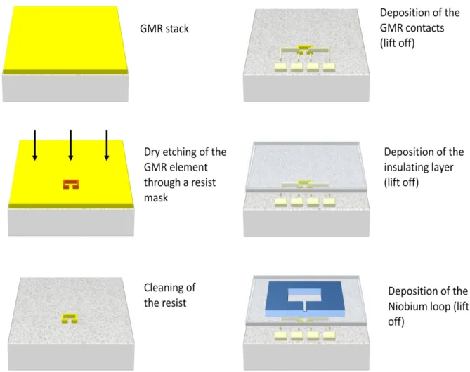
their contact pads. Then an insulating layer is deposited over the surface and the superconducting loop made of Niobium is deposited by a lift off technique. The steps used for fabrication are detailed in Figure 11.
Figure 11: Fabrication steps of a low-Tc mixed sensor (top to bottom, left to right), starting from the GMR stack
21
High-Tc mixed sensor:
The use of high-Tc superconducting loop allows operating the sensor at liquid nitrogen
temperature. As high-Tc thin film requires epitaxial growth conditions on a dedicated
substrate and with a high temperature (>600°C) step, it is necessary to fabricate the sensor from the YBCO film. First step is to deposit a thin and flat insulating layer on the YBCO plain film, then to deposit the GMR stack. Quality of the insulating layer is important: it has to be dense (no holes which would shortcut the structure through the superconductor) and flat (roughness would lead to mismatches between the different layers of the GMR stack, reducing strongly the magnetoresistive effect). When these conditions are fulfilled, the patterning process can be applied, schematically described in Figure 12.
Figure 12: Fabrication steps of a high-Tc mixed sensor (top to bottom, left to right), starting from the GMR
stack deposited on the YBCO film (an insulating layer in between the two).
Another way to proceed is to process the YBCO loop first, then deposit the insulating layer and the GMR stack, which can be processed as usual. This method has been applied successfully by Sensitec [12] to process YBCO-mixed sensor on 5” sapphire-substrate (see Figure 13).
22
Figure 13 : Left : Photograph of a 5” sapphire wafer processed by Sensitec GmbH [12] to produce YBCO-based mixed sensor. The YBCO layer has been deposited by Theva GmbH [13] . Right: Photograph of one device.
Characteristics
The realized mixed sensors can be characterized through two features: the effective gain of the sensor (g) and the noise of the device, which is given by the noise spectrum density of the GMR element. Knowing these two data, we can compare the gain to the calculated value, extract the signal-to-noise ratio as a function of frequency and know the detectivity of the sensor.
Measuring the gain of the sensor
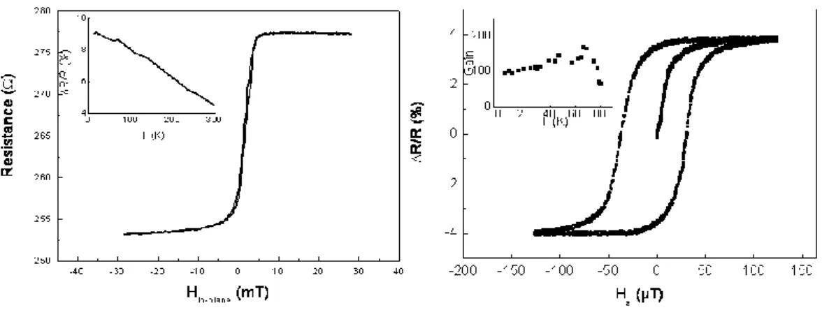
The gain of the sensor can be easily estimated from the comparison of the slope of the GMR element response above Tc in an in-plane field and below Tc in an out-of-plane field.
During the experiment, the GMR response is recorded by sweeping a homogeneous magnetic field up and down in the direction of the pinned layer of the GMR at different temperatures. Below Tc, the same experiment is carried out but with a field applied
perpendicularly to the plane of the loop. The GMR element being insensitive to the z-component (out of plane) of the field, the variation of resistance is only due to the self-field generated by the superconducting screening current. This property can be also used to determine the Tc of the constriction, the response getting weaker when approaching Tc and
zero at and above Tc.
23
Figure 14: Resistance variation of the GMR element for an in-plane field (left) above Tc and an out-of-plane
field (right) below Tc. Note the difference in the magnetic field scale. Insets: Left: ratio as a function of
temperature; Right: variation of the gain g as a function of temperature.
On the operating mixed sensor, a saturation of the magnetoresistance ratio occurs usually before the maximum is reached. This is due to the fact that the critical current is reached in the constriction, and therefore, the induced field does not increase anymore. The effect explains also why at higher field, when sweeping back the field, the MR ratio decreases; according to the Bean model [15] , as soon as the field is reversed, the supercurrent starts decreasing in the superconductor.
The field at which the critical current is reached in the constriction depends on the size of the loop (the larger, the sooner), of the size of the constriction (the smaller, the sooner), of the temperature (the cycle is getting smaller and smaller when approaching Tc) and of the
quality of the material.
The gain can be calculated simply by the ratio of the two slopes, and compared to the calculated gain. As can be seen in Table 2, a very good agreement is obtained on various sensors.
Samples l (mm) Constriction width w (µm)
Calculated gain Measured gain
Nb-100 7 7 131 108
Nb-500 25 6 516 500
YbaCuO 3 6 170 160
YbaCuO 18 5 620 600
YbaCuO 20 3 1100 1060
24
Measuring the noise of the sensor
As the superconducting loop remains in the Meissner state, the main noise source that we expect on the sensor is the noise of the GMR element. The total noise of the sensor can be estimated by measuring the GMR element noise spectrum at low temperature and divide it by the gain g.
The noise spectrum is measured either on the output voltage of a single GMR, either on the output on the GMR bridge or half bridge (in the case of Wheatstone bridge configuration).In the case of a single GMR, the output voltage is balanced from an adjustable equivalent resistance. The differential voltage is sent to a low noise amplifier (INA 103), which allows an amplification of 500 with an additional noise of 1.2 nV/√Hz in the thermal noise. After this first level of amplification, the signal is sent to a second filter-amplifier level (Stanford Research 560), allowing high and low pass filtering, and additional amplification. For low frequency noise measurements, a low pass filter in the 10 kHz range is usually chosen to avoid anti-aliasing of higher frequencies noise. In noise spectrum measurements, all additional sources of noise should be reduced or eliminated. In particular, voltage supply noise can be avoided by feeding the sensor current on battery, as well as the amplification chain. Only the acquisition card is plugged on main power. Use of low temperature electronics (at the first stage of amplification) could reduce the total noise to 0.15 nV/√Hz.
Figure 15: Left: Noise measurement set-up for a single GMR element. Three equivalent resistances are connected, one being adjustable to balance the bridge. Right: Noise measurement setup for a full bridge GMR configuration. The preamplifier (INA 103) has a gain of 500 and the SR560 is set to the maximum gain (up to 1000). A low pass filtering is applied at around 10 kHz to avoid anti-aliasing of higher frequency noise.
Examples of noise spectra and field sensitivities are given in Figure 16.
1 10 100 1000 0.1 1 Field (pT / Hz -1 /2 ) 10 1 1mA 5K 0 mA Voltag e Noise (nV/ Hz -1 /2 ) Frequency (Hz) 0.1 1 10 100 10 100 1000 10000 15mA - 4.2K 5mA - 77K Field (fT / Hz -1 /2) Frequency (Hz)
25
Figure 16: Left: Voltage noise at 4 K for a Nb-based mixed sensor with a 0 mA and a 5 mA sensing current. Right: Field detectivity calculated from the voltage noise spectrum of a YBCO sensor at 4 K (sensing current 15 mA) and 77 K (sensing current 5 mA).
From these spectra, one may observe few characteristics of the noise of the sensors:
First is the importance of the sensing current through the GMR; the higher the sensing current, the better signal-to-noise ratio the sensor will exhibit (in the thermal noise). Limitations in the maximum value of the sensing current are given by the GMR element itself and the operated temperature (currents as high as 15 mA can be used at 4 K or 77 K without destroying the GMR), second limitation being given by the material used for the superconducting loop. For Niobium, the maximum current in the GMR will only be of 1-2 mA, since higher current will bring a local heating of the Niobium constriction and lead to transition to the normal state. This effect is much weaker in the YBCO, which is operated far from its critical temperature.
Secondly, at low frequency, the noise spectra are dominated by the 1/f noise, on which a change in the GMR sensing current will not operate (except to change the 1/f knee frequency value). This noise is strongly dominant below 100-1 kHz and reduces the sensitivity of the sensor in this range. Techniques to reduce this noise are detailed in the next chapter.
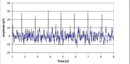
A real measurement of the noise of the sensor can be performed in a magnetically shielding room (MSR). This has been realized in the MSR of Neurospin which contains three aluminium/permalloy shields, and exhibits a residual white noise of the order of few pT (to be compared to few nT in our lab). Recorded data are shown in Figure 17, together with a calibrated 5 pT test signal produced with a small dipolar coil at 30 Hz.
Figure 17: Field equivalent noise recorded in the MSR with a YBCO sensor at 77 K, and with a reference signal of 5 pT at 30 Hz produced by a small dipolar coil. The thermal noise of the sensor is indicated by the plain blue line. Low-Tc Squids detectivity level is indicated by the red plain line.
26
The noise figure provides useful information on the signal-to-noise ratio for various frequencies. Best performances are obtained in the thermal regime, leading to values of few fT/√Hz (see Table 3). At lower frequencies, the noise is dominated by a 1/f contribution, which reduces the detectivity of the sensor to few hundreds of fT/√Hz.
Sample
Measured gain Surface (mm2
) Maximum sensing current Sensitivity at 77 K (fT/√Hz) Sensitivity at 4 K (fT/√Hz) Nb A 108 7x7 1mA n.a. 600 Nb B 500 15x15 1mA n.a. 140 YBCO A 160 9x9 15mA 150 32 YBCO B 600 17x17 10mA 25 5 YBCO C 1300 25x25 10mA 8 1.5
27
Mixed sensors for low frequency
measurements
(The results shown in this chapter –MCG and 1/f noise reduction techniques- are part of the PhD work of Hedwige Polovy)
Low frequency response; sensitivity
Estimated etectivity levels for a YBCO sensor with a gain 1000 are given in Table 4.
Sensor Noise at 1 Hz Noise at 10 Hz Noise at 1 kHz Noise at 10 kHz
YBCO 4K 100mW 100 fT/√(Hz) 30 fT/ √(Hz) 3 fT/ √(Hz) 2 fT/ √(Hz) YBCO 4K 1mW 100 fT/ √(Hz) 30 fT/ √(Hz) 20 fT/ √(Hz) 20 fT/ √(Hz) YBCO 77K 100mW 300 fT/ √(Hz) 100 fT/ √(Hz) 10 fT/ √(Hz) 5 fT/ √(Hz) YBCO 77K 1mW 300 fT/ √(Hz) 100 fT/ √(Hz) 40 fT/ √(Hz) 40 fT/ √(Hz)
Table 4: Estimated detectivity levels for a YBCO sensor with a gain 1000 at 4 K and 77 K, for various frequencies and current sensing. 100 mW (1 mW) corresponds to 10 mA (resp.1 mA) in a typical 1 kOhm GMR.
Flux jumps and vortex avalanches
In some ramping field experiments, when the field is swept rather quickly, some instability can be observed in the MR response (see Figure 18 left), which corresponds to a flux jump or vortex avalanche phenomenon. We can describe these observations using a diffusion model of the vortices and determine the energy dissipated by one vortex through the constriction.
When the magnetic field is applied perpendicular to this ring, a supercurrent appears to prevent the entrance of the magnetic flux in the loop. This effect is limited by the critical current in the small constriction. When the field is increased over this limit, the supercurrent is still limited to its critical value and some flux can enter in the loop. The entrance is done by vortices crossing the point of the loop where the critical current density is firstly reached, i.e the constriction. The number of crossing vortices and their flow are accurately controlled by the applied magnetic field. If the vortex flow is large enough, the dissipated energy is sufficient to warm locally the constriction until the transition temperature of the constriction is reached; this is a local flux jump. The magnetic sensor allows us to monitor the evolution of the supercurrent as a function of time and applied field.
28
Figure 18 : Left: Voltage variation in the MR for an applied field of -15/+15 μT/-15 μT scanned on 100 points. The corresponding field step is 0.6 μT. Right: Number of jumps as a function of the field step applied to the sample for the Nb-B device. The field has been scanned between -10 and +10 μT at different rate.
When the magnetoresistance reaches the maximal value which corresponds to the critical current in the constriction, a sufficiently high and fast increase of the magnetic field induces a transition to the normal state in the constriction which destroys the supercurrent; this effect is detected by a sudden drop of the GMR resistance. After the resistance drops, the constriction returns to the superconducting state in a very short time. If the field is further increased the same effect can occur again. The same phenomenon has been observed on different size samples.
As shown in Figure 18, during a cycling of the applied field, drops occur several times, always followed by an increase of the MR to the saturation. If the MR curve is not perfectly centered, the height of the drop can be different on the upper and lower plateau.
An important parameter in the occurrence and frequency of the drops is the slope of the applied field. This aspect has been studied by changing the height of the field steps (see Figure 18 right). The duration of the steps, monitored by a GHz oscilloscope, is of 500 ns, independently of the step height.
It appears that for steps smaller than 0.15 μT (equivalent to field sweep rate below 0.3 T/s), the system is stable and no drop occurs (area I). In the range of 0.15 μT to 0.45 μT (0.3 to 0.9 T/s), the number of drops increases roughly linearly with the field step height (area II), and then reaches a plateau corresponding to the maximum number of drops possible within a cycle (area III), taking into account the field necessary to reach the critical state again. For higher values, the number of drops increases to reach its maximum value, given by the total applied field divided by the field required to reach the plateau.
In order to understand this dispersion of energy we have modeled the temperature behavior when the vortices cross the constriction. The heat diffusion equation as a function of temperature T and position r is given by:
(19)
where C is the heat capacity, is the heat conductivity, h is the heat transfer coefficient at the interface, d the thickness of the Niobium. P is the power brought by the motion of vortices in the constriction. The heat capacity per unit volume is temperature dependent and varies as
29
, leading to at 4.2K. The heat conductivity
depends on the quality of the niobium and varies with temperature as . From the variation of resistivity from room temperature to low temperature of our sample, we obtain that
The heat transfer coefficient has been experimentally determined to be equal to . From this model, we can estimate the temperature distribution (Figure 19) in the constriction according to three main scenarios: the vortices are passing along one centered path (scenario 1), along two lateral paths (scenario 2) or homogeneously through the constriction (scenario 3).Figure 19 : Temperature distribution in the constriction obtained from a heat diffusion model, for a dissipated energy of 2.15 10-12 J, when the vortices cross the constriction on a single channel centered (plain line/upper scenario), when the vortices cross along two different channels located at the edges of the constriction (dashed line/middle scenario) and when the vortices are homogeneously distributed along the constriction (dotted line/bottom scenario). The inset shows the increase of temperature as a function of time.
From our results, we know that the probability to warm the constriction at a temperature higher than 6.5 K is non zero when more than 15 000 vortices (0.15 μT of extra field applied to the inner surface of the loop) pass within the 500 ns of the field ramping time. We can then deduce that the energy dissipated by each crossing vortex is about 1.4x10⁻¹⁶ J for a 5 μm path, i.e. 2.8x10⁻¹¹ J.m-1. It is also important to note that the simulation predicts a constant value for the maximum temperature after only 50ns. This implies that if the experiment time is larger than 50ns, the good parameter for the stability of the constriction is not the total number of vortices but the number of vortices per second. We can give a critical speed of 3x10¹⁰vortex/s, corresponding to a speed of 0.3
T/s on the main loop. This value is comparable with the field sweep rates of flux jumps observations [14]
For applications, as long as the sensor operates in its linear response regime, and far from the critical current, no flux jumps occurs and the device exhibits no loss of history. In the case of a fast and strong magnetic field is applied (for an NMR experiment), flux jump can occur, leading in Nb device to a reset of the sensor, which is desirable.
30
This phenomenon has been rarely observed in YBCO devices, even close to Tc, since the heat capacity
is much higher than in Nb. Other hysteretic behavior might be observed in these devices, which will be described later.
Biomagnetic signal detection
Biomagnetic signals
Very sensitive magnetometers operating at low frequency are potential candidates for biomagnetic signal measurements. These signals having weak amplitude (few tens of fT to few hundreds of pT), occur at low frequency (1 to 1000 Hz) and are complex, requiring sufficient dynamics (typically more than few kHz). Their detection is therefore very challenging.
Two kinds of biomagnetic signals are of particular interest: magnetic cardiac signals and magnetic neuronal signals. Both of them are generated by the field lines due to the electrical currents circulating in the heart and in the brain neural networks. In both cases the sources are not unique and the resulting field is non uniform, depending on the location and of the distance to the source. Cardiac signals:
In the case of the heart, the signal is due to electric ionic currents in the myocardial membranes, spreading and flowing through the tissues, resulting in electric potentials which can be measured by means of chest electrodes (electrocardiography or ECG) or magnetic fields sensors (magnetocardiography or MCG). The ventricular action potential (AP), measured by ECG through the resulting voltage, or by MCG through the induced magnetic field (Figure 20) presents shape and duration characteristics of the ventricular repolarization (ST segment, T wave, QT interval).
Figure 20 : Schematics of the propagation of the electrical signal in the heart, and resulting electrical component versus time as can be measured on ECG electrodes (from [17] ).
First human MCG have been recorded in 1963 by Baule Mc Fee [18] with a set of copper coils and real-time MCGs have been achieved thanks to low-Tc SQUIDs in 1970 [19] . Since then, mapping systems have been developed, allowing vector reconstruction in time. This technique is
31
complementary to the widely used ECG. It provides more information on specific dysfunctions like ischemia, which may not be properly detected in ECG. As no electrodes are used, this technique presents a non negligible advantage in burns unit. Furthermore, active research using MCG is purchased for the third semester pregnancy cardiac monitoring, where cardiac anomalies are difficult to detect (at this stage, the fetus is protected by the vernix caseosa which is an insulating grease and does not permit recording of the electrical signal via ECG electrodes). Even though MCG systems are much more expensive than ECG and require often a shielded environment, the mapping function and non contact aspect represent large potentiality for systematic population studies. A system which would combine MCG together with non invasive anatomic information (ultrasound or low-field MRI) would be a great tool in hospital environment.
Neuronal signals:
Neuronal activity produces a constant flow of information generated and carried through electrical signals via neurons and synapses. Neural signals are coded in frequency modulation of Action Potential (AP) occurrences. The duration of the AP is of 2-3 ms, with typical frequencies of 0.1 to 100 Hz, propagation speed being of the order of 100 m/s. Like for the cardiac signals, electrical neural signals can be recorded with electrodes on the scalp (electro-encephalography or EEG). The propagating AP is generating some magnetic field lines which can be detected outside of the brain since the human body is transparent to magnetic fields. Magneto-encephalography (or MEG) consists in recording this signal through extremely sensitive sensors (commercially only low-Tc SQUIDs are used for this purpose) usually arranged in arrays of sensors, up to more than 300 devices, in magnetometer and/or gradiometer configuration. They allow getting information on the magnitude and vector components of the field. Solutions to the inverse problem must be obtained to localize the source and get the relevant information (position, feature, time evolution).
In MEG, the sensors are more sensitive to tangential sources, whereas in EEG, radial sources give the dominant signal. The information obtained by both techniques are therefore different depending on the location of the source (sulci or gyri for instance).
Figure 21 : Left: two type of dipoles, oriented tangentially to the skull (in the sulci) or radially (in the gyri) which can be seen both in EEG, whereas MEG only sees the tangential source (from [21] ). Right: Magnetic field and electric potential patterns produced by a tangential dipole (arrow) (from [20] ).
MEG is used in clinical and cognitive research. Presurgical mapping of the functions of the brain can be used prior to surgery in some cases of strong epilepsy. Widely used in cognitive sciences, MEG allows temporal information on the normal and pathologic brain functioning. Studies about language, memory, consciousness, sensory-motor functions have been carried out on adults and children. Population with a neurological disorder such as schizophrenia, dementia, Parkinson, Alzheimer, just to cite few, have been studied with this tool.
32
Precise information in time (in the ms range) and location (few mm3) are the main advantages of this non invasive technique, applicable on wide range of population. This is nowadays one of the major tools with functional MRI to study the human brain functions.
Figure 22 : Left panel: commercial MEG system produced by Elekta Neuromag; Right panel: Top: schematics of the 306 SQUID devices around the head of the subject in the Elekta system. Bottom: typical magnetic response to auditory stimuli of 50 ms (hatched area), measured close to the subject’s auditory cortex (from [20] ).
First biomagnetic measurements with a mixed sensor
As our sensors have demonstrated noise level of less than 1 pT in the 1/f regime (see Figure 17), it is possible to apply them to MCG signal recording. Due to the very small amplitude of the signals with respect to the environmental noise, it is necessary to operate the experiment in a shielded environment. The experiments have been carried out in the Magnetic Shielded Room (MSR) at Neurospin MEG facility with Nb and YBCO-based mixed sensor. The cryostats used for these experiments are home-made fiberglass dewars, where the sensor is directly placed in the cryogenic liquid (helium or nitrogen). Schematic of the experiment is given in Figure 23.
33
Figure 23 : Left: Schematic of the MCG experiment. Right: Picture of the experimental setup (fiberglass dewar and low-noise amplifier) on the right in Neurospin MSR. The commercial MEG system is visible on the left of the picture.
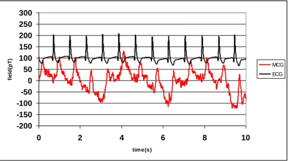
Simultaneous recording of the ECG with chest electrodes have been done. Raw signals and averaged signals are given in Figure 24 and Figure 25.
Figure 24 : Raw MCG signal recorded on a Nb-mixed sensor with a thermal noise of 100 fT/√Hz.
Figure 25 : Averaged (30 times) MCG signal. QRS complex and T-wave are well visible.
-20 -10 0 10 20 30 40 1 2 3 4 5 6 7 8 9 temps(s) a m p li tu d e ( p T ) Time (s) -10 -5 0 5 10 15 20 25 0 0.2 0.4 0.6 0.8 1 temps(s) a m pl it ud e ( pT ) Time (s)
34
Similar experiments have been performed with high-Tc mixed sensors at 77 K, demonstrating the
performances of the sensor in this range of field and frequency.
Recording (also) the artifacts and ballistocardiography
As mixed sensors are sensitive to any magnetic field present in the environment, it occurs sometimes that during the experiment some artifacts generate signals stronger than the MCG signal. One common artifact is the presence of a ferromagnetic contaminant on the subject, for instead slightly magnetic ECG electrodes. In this case, a large and slow oscillation, fitting to the breathing of the subject, induces a very low frequency signal (Figure 26) corresponding to the motion of the contaminant.
Another artifact, more difficult to identify may occur, which is due to ballistocardiography (BCG). When the heart beats, the blood flow sent by the artery to the ends of the body induces a very small motion of the body itself, at a frequency of a cardiac pulse, i.e. at the same frequency as the electrical heart signal. This is the ballistocardiographic effect [22] . If a ferromagnetic material is present on the clothes or on the body of the subject, this pulsed motion of the body will induce a motion of the small magnetic object. One way to identify it is that this artifact will show various patterns when changing the sensor’s position (Figure 27).
Figure 26 : Raw ECG (black) and MCG (red) data recorded simultaneously. The strong oscillation in the MCG corresponds to the breathing of the subject. This is probably induced by the motion of small ferromagnetic material present on the subject (here probably the ECG electrodes).
-200 -150 -100 -50 0 50 100 150 200 250 300 0 2 4 6 8 10 tim e(s) fi e ld (p T ) MCG ECG
35
Figure 27 : MCG signals for various locations of the sensor over the subject’s torso. The magnetic patterns, very different from one position to another is due to the presence of a ferromagnetic contaminant (i.e. nickel pants button) which is slightly displaced by the blood heart beat and therefore gives a magnetic signature at the same frequency as the MCG and ECG, but with a complex field line pattern.
Discussion on biomagnetic measurements with a mixed sensor
Limitations to the performances of the devices at this point are the following: - Noise of the pre-amplifier:
We have used a room temperature low noise preamplifier INA 103, with a thermal noise of 1.2nV/√Hz. For the lowest frequencies (<1kHz), the noise of the GMR elements are strongly dominant (by 1 to 2 orders of magnitude, depending on the frequency), but if the sensor sensitivity increases, the amplifier noise may contribute. Therefore we have started to implement cold preamplifier made out of SiGe transistors provided by Mikko Kirivanta at VTT, Finland. These devices should have an intrinsic noise of only 170pV/√Hz.
- Environmental noise:
The sensors have been used as magnetometers with no reference point. They are therefore sensitive to all sources of external noise, including the residual environmental noise present in the Magnetically Shielded Room. To increase the amplitude of the relevant signal (MCG or later on MEG), one could work in gradiometric mode, with a sensor afar from the source, which would record the residual noise in order to subtract it on the primary sensor (closest to the relevant source). This method is widely used for SQUIDs and in some cases allows working in a lighter shielding environment or no shield at all.
- 1/f noise:
As it has been seen in Part II, the main source of noise of the sensor at low frequencies is the 1/f noise. To get sensitivity of tens of femtotesla, needed for MEG, with the present sensors, one should find ways to reduce or cancel this noise. This point is developed in the next section.
1/f reduction techniques
This 1/f noise is given by the GMR element, which is of small volume. In order to reduce this
-100 -80 -60 -40 -20 0 20 40 60 80 0 0.1 0.2 0.3 0.4 0.5 0.6 0.7 0.8 ECG MCG1 MCG2 MCG3
36
contribution, modulation techniques can be developed and applied. Simple current modulation would not be effective since the sensor is linear. Modulation of sources cannot be applied due to the nature of the signal sources (biomagnetic sources or NMR signals). Modulation can however be applied by switching the sensor in two configurations, one where the sensor operates and records the signal, and one configuration where the sensor is set to blank. This can be achieved by saturating the sensor or by acting on the state of the superconducting loop of the sensor (open or closed). Indeed if one cuts the supercurrent path in the loop, the sensor will not be sensitive to the applied flux, and will be set to zero change in the magnetoresistance.
Saturating the supercurrent
One idea to modulate the sensor is to reach a reference point. This can be achieved by reaching the critical current in the constriction. At this point, the sensor is not sensitive anymore to any external field variation. One way to achieve this is to apply an extra field which will drive the sensor to the saturated state, but this technique leads to a loss of history of the sensor. Another way is to inject a current in the loop to reach the critical current in the constriction, and so a reference point. It can be very fast and work easily, but the absolute field reference is also lost and the information obtained will be only the derivative of the signal, not the signal itself.
Local heating technique
A local heating of the constriction can be achieved by driving a sufficiently high current on a local point of the constriction (as can be seen in
Figure 28
). This local heating can be performed in the kHz range, leading to a modulation of the sensor at a frequency which corresponds to the thermal noise. If two constrictions are mounted in parallel, switching on and off the heating of these constrictions leads to a modulation of the supercurrent without destroying it. An example of this modulation is shown inFigure 28
. A 30 Hz sinusoidal signal of 100 nT is recorded by the sensor on which an alternating heating is performed. One can see from the experimental curve that the external signal is modulated at the frequency of the heating pulses. Such techniques can get the sensor sensitivity at low frequency to be increased by one to two orders of magnitude.Figure 29
shows the noise measured with and without the modulation.Figure 28: Left: Micrograph of two GMR elements (C shaped) mounted in bridge configuration and heating contact lines. Right: 100 nT peak to peak signal created by a small coil and detected by a magnetoresistive hybrid sensor with a toggle of the supercurrent running in the loop. The curve gives the signal detected by one of the GMR element in the bridge.
37
1
10
100
1000
0,01
0,1
1
10
F
ield
det
ec
tiv
it
y
(pT
/
Hz)
Frequency (Hz)
direct toggleFigure 29: Low frequency noise without (dark grey) and with (light grey) modulation. The peak at 30 Hz corresponds to a test signal in a small external copper coil.
This technique has some drawbacks: the current required to heat the constriction is of several mA or tens of mA, and if the stray fields generated by this current on the superconducting loop can be cancelled by symmetrizing the contact lines, capacitive effect occurs through the insulating layer and the superconductor to the GMR, leading to strong peaks in the magnetoresistance when the heating pulse is on. This effect might be a limitation to the efficiency of this technique.
Another idea therefore is to use a local non electrical heating by a laser probe. Schematics of the experiment is shown in Figure 30.
The laser is a 140 nm pulsed diode which can provide a power up to 1 W. The diameter of the probe at the output (1 mm) can be focused by means of optical lenses to part of the constriction. For this experiment, a new design of the sensor, with a longer constriction is required, but first tests will consist in testing the condition in which the mixed sensor is set to zero and recovers from the laser pulse (duration, power, repetition rate…).
38
Figure 30 : Schematics of the 1/f noise cancellation technique with a laser probe.
Conclusion
In conclusion of this part on the low frequency range, mixed sensors already exhibit sensitivity in the picotesla range at very low frequency, and can be already applied for MCG recordings. Improvements of the sensitivity at low frequency can be achieved by dedicated modulation techniques, opening road for MEG recordings with mixed sensors at 77 K.

![Figure 13 : Left : Photograph of a 5” sapphire wafer processed by Sensitec GmbH [12] to produce YBCO-based mixed sensor](https://thumb-eu.123doks.com/thumbv2/123doknet/14711171.748930/23.892.138.722.105.346/figure-left-photograph-sapphire-processed-sensitec-produce-sensor.webp)