HAL Id: tel-01689976
https://tel.archives-ouvertes.fr/tel-01689976
Submitted on 22 Jan 2018HAL is a multi-disciplinary open access archive for the deposit and dissemination of sci-entific research documents, whether they are pub-lished or not. The documents may come from teaching and research institutions in France or abroad, or from public or private research centers.
L’archive ouverte pluridisciplinaire HAL, est destinée au dépôt et à la diffusion de documents scientifiques de niveau recherche, publiés ou non, émanant des établissements d’enseignement et de recherche français ou étrangers, des laboratoires publics ou privés.
photovoltaics applications
Shanting Zhang
To cite this version:
Shanting Zhang. Study of fluorine-doped tin oxide (FTO) thin films for photovoltaics applications. Materials. Technische Universität (Darmstadt, Allemagne), 2017. English. �NNT : 2017GREAI021�. �tel-01689976�
Doctoral Thesis
To obtain the academic doctoral double-degree joint by Communauté Université Grenoble Alpes (UGA) and
Technische Universität Darmstadt (TU Darmstadt)
Under the framework of International Doctoral School in Functional Materials (IDS-FunMat)
Prepared by
Shanting Zhang
Supervised by Daniel Bellet and Andreas Klein, co-supervised by David Muñoz-Rojas
in Laboratoire des Matériaux et du Génie Physique (LMGP, UGA) and Surface Science division (TU Darmstadt)
Study of fluorine-doped tin
oxide (FTO) thin films for
photovoltaics applications
Public oral defense on March 23, 2017 with jury members:
Prof. Dr. Patricia Segonds
Professor of Université Grenoble Alpes, Institut Néel (President) Prof. Dr. Bruno Masenelli
Professor of institut national des sciences appliquées de Lyon (Reporter) Prof. Dr. Alain Billard
Professor of Université de technologie de Belfort-Montbéliard (Reporter) Prof. Dr. Ulrike Kramm
Professor of Technische Universität Darmstadt (Co-referee) Prof. Dr. Wolfgang Ensinger
Professor of Technische Universität Darmstadt (Examiner) Prof. Dr. Daniel Bellet
Professor of Université Grenoble Alpes, LMGP (Supervisor) Prof. Dr. Andreas Klein
Professor of Technische Universität Darmstadt (Co-supervisor/referee) Dr. David Muñoz-Rojas
THÈSE
Pour obtenir le grade de
DOCTEUR DE LA COMMUNAUTE UNIVERSITE GRENOBLE ALPES
préparée dans le cadre d’une cotutelle entre la Communauté
Université Grenoble Alpes et Technische Universität Darmstadt
Spécialité : Matériaux, Mécanique, Génie civil, Electrochimie
Arrêté ministériel : le 6 janvier 2005 - 7 août 2006
Présentée par
Shanting Zhang (张姗婷)
Thèse dirigée par Daniel Bellet et Andreas Klein codirigée par David Muñoz-Rojas
préparée au sein des Laboratoire des Matériaux et du Génie Physique (LMGP) et Surface Science division (TU Darmstadt) dans l’Ecole Doctorale Ingénierie – Matériaux, Mécanique, Environnement, Energétique, Procédés, Production (I-MEP2)
Study of fluorine-doped tin
oxide (FTO) thin films for
photovoltaics applications
Thèse soutenue publiquement le 23/Mars/2017, devant le jury composé de :
Mme. Patricia Segonds
Professeur à Université Grenoble Alpes, Institut Néel (Président) M. Bruno Masenelli
Professeur à institut national des sciences appliquées de Lyon (Rapporteur) M. Alain Billard
Professeur à Université de technologie de Belfort-Montbéliard (Rapporteur) Mme. Ulrike Kramm
Professeur à Technische Universität Darmstadt (Invitée) M. Wolfgang Ensinger
Professeur à Technische Universität Darmstadt (Invité) M. Daniel Bellet
Professeur à Université Grenoble Alpes, LMGP (Directeur de thèse) M. Andreas Klein
Professeur à Technische Universität Darmstadt (Co-directeur de thèse) M. David Muñoz-Rojas
Study of fluorine-doped tin oxide (FTO)
thin films for photovoltaics applications
Dissertation approved by the department of Materials and Geoscience
Technische Universität Darmstadt
Requirements to obtain the academic degree of
“Doctor rerum naturalium” (“Dr. rer. nat.”)
Approved dissertation by Shanting Zhang, M. Sc.
from
Zhejiang, People’s Republic of China
Primary referee: Prof. Dr. Andreas Klein
Secondary referee: Prof. Dr. Ulrike Kramm
Date of Submission: January 16, 2017
Date of oral defense: March 23, 2017
Darmstadt 2017
D17
Study of fluorine-doped tin oxide (FTO) thin films for
photovoltaics applications
Doctoral dissertation by Shanting Zhang (张姗婷), M. Sc.
This is a double-degree doctoral thesis joint byUniversité Grenoble Alpes (UGA, France) and
Technische Universität Darmstadt (TU Darmstadt, Germany) under the framework of
International Doctoral School in Functional Materials (IDS-FunMat)
Supervisor: Prof. Dr. Daniel Bellet (Université Grenoble Alpes)
Co-supervisor: Prof. Dr. Andreas Klein (Technische Universität Darmstadt) Co-supervisor: Dr. David Muñoz-Rojas (CNRS researcher)
Please cite this document as:
urn:nbn:de:tuda-tuprints-61265
http://tuprints.ulb.tu-darmstadt.de/id/eprint/6126
The publication is licensed under the following Creative Commons license: Attribution – No commercial use – No derivatives 4.0 International
Erklärung zur Dissertation
Hiermit versichere ich, die vorliegende Dissertation ohne Hilfe Dritter nur mit den angegebenen Quellen und Hilfsmitteln angefertigt zu haben. Alle Stellen, die aus Quellen entnommen wurden, sind als solche kenntlich gemacht. Diese Arbeit hat in gleicher oder ähnlicher Form noch keiner Prüfungsbehörde vorgelegen.
Grenoble, den Januar 19, 2017
(Shanting Zhang)
Author Declaration
I hereby declare that this thesis is my own work and effort. This is a true copy of the thesis, including any required final versions, as accepted by my examiners. I understand that my thesis may be made electronically available to the public.
Grenoble, January 19, 2017
To my family
To Wenbo
Acknowledgement
First of all, I’d like to thank my family who have supported me all the way along. The summer when I traveled Spain and Italy with my mom and my sister was really the best summer ever! I sincerely thank my supervisors Daniel Bellet and Andreas Klein, as well as David Muñoz-Rojas for their help and support to overcome all the difficulties and put together all the pieces to make this project finally work.
I spent most of my time in LMGP where I completed the majority of the work in this thesis. Everyone in LMGP has supported me in a way or two during the past three years. I thank Franz Bruckert, Michèle San Martin, Josiane Viboud, Virginie Charrière, and Arnaud Robin for their help concerning the administrative and technical issues; I thank Carmen Jiménez, Jean-Luc Deschanvres, Matthieu Jouvert, Hervé Roussel, Laetitia Rapenne, Etienne Pernot, Odette Chaix, Michel Langley, and Vincent Consonni for their help on the experimental setup, sample characterizations as well as the many fruitful scientific discussions. Their time and efforts are indispensable for my thesis to proceed smoothlyν I’m also thankful for all the other members of LMGP who have contributed to my work/living via different manners.
According to the IDS-FunMat project, I also have the chance to stay in the surface science group where I not only enriched my scientific understanding, but also get to know nice people. I thank Marga Lang and Leslie Frotscher for taking care of the paper work and making my life easier. I thank Erich Golusda and Joachim Brötz for their experimental help. Many thanks to all the people from the oxide group for the valuable advices and discussions: Mirko Weidner, Hans Wardenga, Jan Morasch, Stephan Hillmann, and Christian Lohaus.
Additionally, this thesis has involved collaborations with many different people/labs. I thank Guy Vitran from IMEP-LaHC for his contribution on the optical simulation as well as the many useful discussions; I thank Martin Foldyna from LPICM for welcoming and helping me with various optical experiments including ellipsometry, ARTA and ARMMP measurements; I also thank Jean-Luc Rouvière from CEA for the STEM measurement and the innovative N-PED technique as well as the results analyses. I thank professor Lukas Schmidt-Mende from University of Konstanz for providing us the S:TiO2 nanoparticles and
the help in integrating the FTO nanocomposites in organic solar cells. I thank Yann Pellegrin and Daniel Langley for their help on fabricating DSSCs on FTO nanocomposites. I thank Giray Kartopu from Glyndŵr University for the various trials of making CdTe solar cells on the FTO nanocomposites.
Finally, I’d like to thank all the IDS-FunMaters that I have met during the international school who have shared their stories and encouraged me all the way along. I wish the best for all of you! Last but not least, thank all my friends who I bear their names with all the good memories in my heart.
Abstract
With the increasing demand for energy that human beings are faced with, the photovoltaics (PV) technology which converts solar radiation into electricity has undergone increasingly development. Although the current PV market is mainly dominated by the crystalline Si based technologies, thin film PV still bears the hope to become the solution to the energy crisis in the future due to its much lower cost and reasonable efficiency.
Transparent conductive materials (TCMs), mostly transparent conductive oxides (TCOs), are an essential component in most types of thin film solar cells as the current-collecting electrode on the sun-facing side of the cell. In order to improve the optical absorption (which is restricted by the limited absorber thickness) in thin film solar cells, the TCOs are often desired to be textured (with significant surface roughness) to show high values of haze factor. Haze factor is defined as the ratio of the diffuse transmittance/reflectance to the total transmittance/reflectance. The hazier a TCO is (i.e. with higher haze factor), the more light it scatters. As a consequence, the optical path length is increased and thus the light trapping in the solar cell is improved, giving rise to higher light absorption in the active layers and photon-to-current conversion efficiency of the solar cells.
In this work, innovative nanocomposites of fluorine doped SnO2 (FTO) in combination with
ZnO, S:TiO2 and Al2O3 nanoparticles have been developed using an economic and facile
2-step process. These FTO nanocomposites exhibit 70-80% total transmittance and 10-15 Ω/sq sheet resistance, satisfying the basic requirements as transparent conductive oxides used in photovoltaics devices. By changing the nanoparticle suspension concentration, the haze factor of these nanocomposites can be varied, in a controlled way, from almost 0% up to 80%. The morphological, structural, electrical, and optical properties of these FTO nanocomposites are investigated in great details and are found to be closely related to the underlying nanoparticles. Before discussing the integration of the FTO nanocomposites into real solar cell devices, efforts have also been made to shed some light on the understanding of FTO/TiO2 interface
commonly adopted in various types of emerging thin film solar cells such as dye sensitized solar cells (DSSCs). Finally, the hazy FTO nanocomposites have been used as transparent electrodes in different types of thin film solar cells and the effect of haze factor on the device performance has been examined.
By properly tuning the type and concentration of the underlying nanoparticles, the properties of the FTO nanocomposites can be tuned to meet the electrode requirement for specific photovoltaic technology. Our concept of preparing TCO nanocomposite by combining TCOs and nanoparticles provides a general guideline to design hazy electrodes as light management structures in thin film photovoltaics.
Résumé
Avec la demande toujours croissante d'énergie à laquelle l’homme fait face, le photovolta₂que (PV), qui convertit le rayonnement solaire en électricité, a connu ces dernières décennies un développement important. Bien que le marché PV actuel soit principalement dominé par les technologies à base de Si cristallin, la technologie PV à base de couches minces porte toujours l'espoir de contribuer efficacement à l'avenir vis-à-vis de la crise énergétique en raison de son coût beaucoup plus faible et d'une efficacité raisonnable.
Les matériaux transparents conducteurs (TCM), principalement des oxydes conducteurs transparents (TCO), sont une composante essentielle dans la plupart des types de cellules solaires à couches minces car ils servent d'électrode de collecte des porteurs photo-générés sur la face avant de la cellule, c’est-à-dire celle face au soleil. Afin d'améliorer l'absorption optique (limitée par l'épaisseur de l'absorbeur) dans des cellules solaires à couches minces, on souhaite souvent que les TCO soient texturés (avec une rugosité de surface significative) de manière à bien diffuser la lumière, et ainsi de présenter des valeurs élevées de facteur de diffusion de la lumière. ωe dernier, que l’on peut appeler facteur de haze, est défini comme le rapport entre la transmittance (respectivement réflectance) diffuse et la transmittance (respectivement réflectance) totale. Plus ce facteur est élevé plus le TCO diffuse la lumière. Par voie de conséquence, la longueur du trajet optique est augmentée et ainsi le piégeage de la lumière dans la cellule solaire est amélioré, donnant lieu à une absorption de lumière plus importante dans les couches actives et augmentant potentiellement le rendement de conversion photovoltaïque des cellules solaires.
Dans ce travail, des nano-composites innovants à base de SnO2 dopé au fluor (FTO) en
combinaison avec les nanoparticules ZnO, S:TiO2 et Al2O3 ont été développés en utilisant un
processus économique et facile constitué de deux étapes. Ces nano-composites à base de FTO présentent une transmittance totale de 70-80% et une résistance de 10-1η Ω/sq, satisfaisant ainsi aux exigences requises pour des oxydes transparents conducteurs utilisés au sein de dispositifs photovoltaïques. En modifiant la concentration de la suspension de nanoparticules le facteur de haze de ces nano-composites peut être varié, de manière contrôlée, de presque 0% à 80%. Les propriétés morphologiques, structurales, électriques et optiques de ces nano-composites à base de FTO sont étudiées en détail et elles apparaissent étroitement dépendantes des nanoparticules sous-jacentes. Avant de discuter de l'intégration des nano-composites FTO au sein de cellules solaires, des efforts ont également été consacrés à une bonne compréhension de l'interface FTO/TiO2 qui est couramment présente au sein de divers
types de cellules solaires à couches minces émergentes telles que les cellules solaires sensibilisées au colorant (DSSCs). Enfin, les nano-composites FTO diffusants ont été intégrés comme électrodes transparentes au sein de différents types de cellules solaires à couches minces et l'effet du facteur de haze sur la performance du dispositif a été étudié.
propriétés des nano-composites à base de FTO peuvent être variées de manière à répondre aux exigences d'électrodes pour une technologie photovoltaïque spécifique. Notre concept de préparation du TCO nano-composite en combinant les TCO et les nanoparticules propose une ligne directrice générale qui conduit à l’élaboration d’électrodes à caractère diffusant variableν permettant ainsi une bonne absorption des photons pour le photovoltaïque en couches minces.
Zusammenfassung:
Die steigende Bedarf der Menschheit an Energie hat zu einer Entwicklung unterschiedlicher photovoltaischer (PV) Technologien, die Sonnenlicht in elektrische Energie umwandeln, geführt. Gegenwärtig dominieren Technologien basierend auf kristallinem Silizium den PV Markt. Dünnschichttechnologien können in der Zukunft zur Lösung der Energiekrise durch ihre geringen Kosten bei geeigneten Wirkungsgraden beitragen
Transparente leitfähige Materialien (TCM), meistens transparente leitfähige Oxide (TCO), sind als stromsammelnde Elektrode auf der lichtzugewandten Seite ein wesentlicher Bestandteil von Dünnschichtsolarzellen. Um die Lichtabsorption, die durch die Schichtdicke der absorbierenden Schicht begrenzt ist, zu erhöhen, ist es wünschenswert texturierte TCO einzusetzen, die eine nennenswerte Oberflächenrauheit und damit eine erhöhte diffuse Streuung (Haze) aufweisen. Der Haze-Faktor ist als das Verhältnis des diffus transmittierten bzw. reflektierten Lichts zum gesamten transmittierten bzw. reflektierten Licht definiert. Ein höherer Haze-Faktor führt daher zu einer erhöhten Streuung des Lichts und erhöht damit die optische Weglänge des Lichts im Absorbermaterial. In der aktiven Schicht wird damit ein höherer Anteil des Lichts absorbiert, was in einer höheren Stromausbeute der Solarzelle resultiert.
In dieser Arbeit wurden innovative Nano-Komposite von fluor-dotiertem SnO2 (FTO) mit
ZnO, S:TiO2 und Al2O3 Nanopartikeln über einen wirtschaftlichen und einfachen
zweistufigen Prozess entwickelt. Die FTO Nano-Komposite weisen 70-80% Transmission und einen Schichtwiderstand von 10-15 Ω/sq auf und erfüllen damit die wesentlichen Anforderungen an ein TCO in photovoltaischen Bauteilen. Der Haze-Faktor der Nano-Komposite kann über die Konzentration der Nanopartikel in der Lösung in kontrollierter Weise zwischen nahezu 0% und 80% eingestellt werden. Die morphologischen, strukturellen, elektrischen und optischen Eigenschaften der FTO Nano-Komposite wurden detailliert untersucht. Diese hängen eng mit den verwendeten Nanopartikeln zusammen. Experimente zum besseren Verständnis der FTO/TiO2 Grenzfläche, die in verschiedenen Typen neuer
Dünnschichtsolarzellen, wie zum Beispiel farbstoff-sensibilisierte Solarzellen (DSSC), verwendet wird, werden ebenfalls in der Arbeit beschrieben. Desweiteren wurde das Verhalten der diffus streuenden FTO Nanokomposite und der Einfluss des Haze-Faktors als transparente Elektrode in verschiedenen Dünnschichtsolarzellen untersucht.
Durch geeignete Variation des Typs und der Konzentration der Nanokomposite können die Eigenschaften der FTO Nanokomposite gezielt eingestellt werden, um die spezifischen Anforderungen an die Elektroden in unterschiedlichen Photovoltaik-Technologien zu erfüllen. Das Konzept der Präparation von TCO Nanokompositen durch Kombination von TCOs und Nanopartikeln bietet eine allgemeine Grundlage zum Design diffus streuender Elektroden für das Lichtmanagement in der Dünnschichtphotovoltaik.
Table of content
List of abbreviations ... i
Symbols and physical quantities ... iii
Preface ... 1
Chapter 1. Introduction ... 4
1.1 Energy and Photovoltaics: Overview ... 4
1.2 Basics of Semiconductors ... 13
1.2.1 Electronic structure of atoms ... 13
1.2.2 Band structure ... 14
1.2.3 Electrons and holes ... 17
1.2.4 Doping ... 21
1.2.5 Quasi-Fermi level ... 22
1.3 Physics of Solar Cells ... 24
1.3.1 Basic process in solar cells ... 24
1.3.2 p-n junction ... 28
1.3.3 Important solar cell parameters ... 31
1.4 Transparent Conductive Materials (TCMs) ... 32
1.4.1 Transparent Conductive Oxides (TCOs) ... 32
1.4.2 F-doped SnO2 (FTO) ... 39
1.4.3 Emerging TCMs ... 41
1.5 Light trapping in solar cells ... 42
1.5.1 Light trapping in thin film Si solar cells ... 42
1.5.2 Light trapping in DSSCs ... 47
1.6 The blocking TiO layer in DSSCs ... 49
1.7 Scope of the Thesis ... 51
Reference ... 52
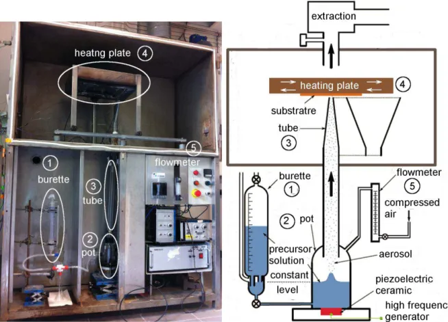
Chapter 2. Experimental Details ... 62
2.1 Fabrication of FTO nanocomposites ... 62
2.2 Deposition of b-TiO thin layers ... 64
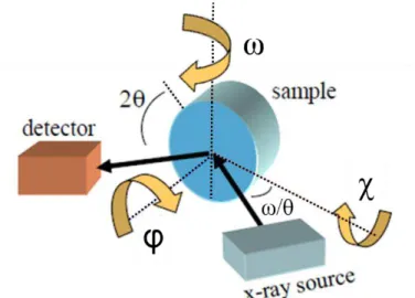
2.3.1 X-Ray Diffraction ( -β , GIXRD, ω-scan, pole figure, RSM) ... 65
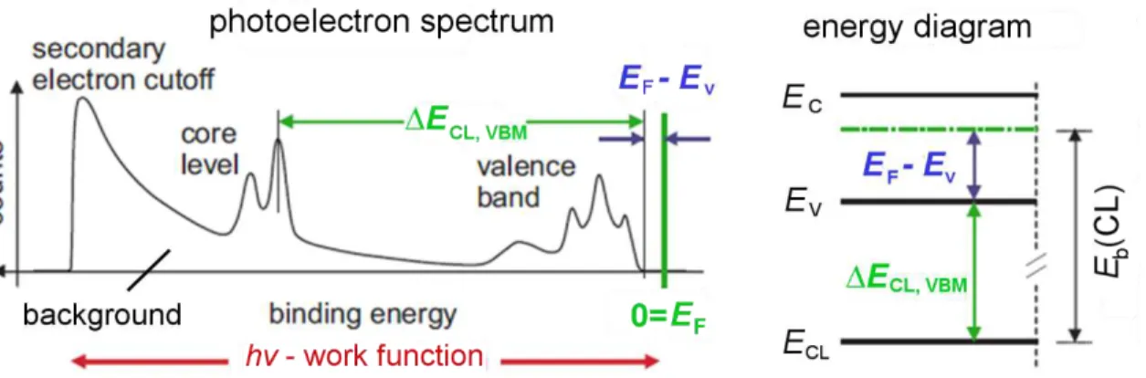
2.3.2 X-ray photoelectron spectroscopy (XPS) ... 70
Techniques based on interaction with electrons ... 75
2.3.3 Scanning Electron Microscopy (SEM) ... 75
2.3.4 Transmission Electron Microscopy (TEM) ... 77
Laser based techniques ... 79
2.3.5 Atomic Force Microscopy (AFM) ... 79
2.3.6 Raman Spectroscopy ... 80
Light based techniques ... 81
2.3.7 Optical Microscopy ... 81
2.3.8 UV-Vis-NIR Spectrophotometer ... 81
2.3.9 Angle-resolved Mueller matrix polarimeter (ARMMP) ... 83
Electrical measurements ... 84
2.3.10 Four-point probe ... 84
2.3.11 Hall-effect measurement ... 85
Reference ... 86
Chapter 3. Morphology and Structural Properties of FTO nanocomposites ... 88
3.1 Morphology of FTO nanocomposites ... 89
3.1.1 Morphology of nanoparticle substrates ... 89
3.1.2 Morphology of FTO nanocomposites ... 91
3.2 Structural properties of FTO nanocomposites ... 97
3.2.1 Texture evolution of ZnO-FTO, S:TiO2-FTO and Al2O3-FTO nanocomposites . 97 3.2.2 Structural analyses of S:TiO2 nanoparticles/substrates ... 105
3.3 Proof of local epitaxial growth of FTO on rutile S:TiO nanoparticles ... 108
3.3.1 Direct cross sectional TEM observation ... 108
3.3.2 Epitaxial FTO films grown on (110) rutile TiO2 single crystals ... 109
3.3.3 Strain and defect structure in the epitaxial FTO films ... 114
3.3.4 Morphology and electrical properties of epitaxial FTO films ... 121
3.4. Conclusions and Perspectives ... 124
4.1 Electrical properties of FTO nanocomposites ... 131
4.2 Optical properties of FTO nanocomposites ... 133
4.2.1 Optical transmission: Ttot and HT ... 133
4.2.2 Angle resolved scattering (ARS) with automated reflectance/transmittance analyzer (ARTA) module ... 138
4.2.3 Angle-resolved Mueller matrix polarimeter (ARMMP) ... 140
4.3 Optical simulation ... 145
4.3.1 Optical scattering by a single nanoparticle agglomerate ... 145
4.3.2 Optical scattering of FTO nanocomposites ... 151
4.4 Conclusions and Perspectives ... 157
References ... 159
Chapter 5. FTO/TiO2 interface in Photovoltaic Devices... 161
5.1 b-TiO layers grown on FTO and Si substrates ... 162
5.1.1 b-TiO2 layers deposited by the SolGel method ... 162
5.1.2 b-TiO2 layers deposited by AA-MOCVD ... 167
5.2 b-TiO layers deposited on RuO by SolGel method ... 171
5.3 Energetic alignment at FTO/b-TiO interface ... 173
5.4 Conclusions and Perspectives ... 177
Reference ... 179
Chapter 6. Device integration ... 182
6.1 FTO nanocomposites in dye-sensitized solar cells (DSSCs) ... 183
6.2 FTO nanocomposites in Cd ₋ₓ Zn ₓ S/CdTe solar cells ... 186
6.3 FTO nanocomposites in organic solar cells ... 191
6.4 Conclusions and Perspectives ... 195
References ... 196
i
List of abbreviations
a-Si: amorphous silicon
a-Si:H: hydrogenated amorphous silicon b-TiO2: blocking TiO2
c-Si: crystalline silicon
nc-TiO2: nanocrystalline TiO2
mono c-Si : monocrystalline silicon, equivalent to single crystalline silicon (sc-Si) multi c-Si: multi-crystalline silicon, equivalent to polycrystalline silicon (poly c-Si)
c-Si: microcrystalline silicon poly-Si: polycrystalline silicon
AA-MOCVD: aerosol assisted metal organic chemical vapor deposition AFM: atomic force microscopy
ARMMP: angle-resolved Mueller matrix polarimeter ARTA: automated reflectance transmittance analyzer ATO: antimony doped tin oxide
AZO: aluminum doped zinc oxide BSE: back scattered electron CB: conduction band
CBM: conduction band minimum CdTe: cadmium telluride
CIGS: copper indium gallium diselenide CIS: copper indium selenide
CL: core level
CVD: chemical vapor deposition DOS: density of states
DSSC: dye-sensitized solar cells
EBSD: electron back scattered diffraction EQE: external quantum efficiency
ii FoM: figure of merit
FTO: fluorine doped tin oxide IR: infrared
IS: integrating sphere
ITO: tin doped indium oxide
LCAO: linear combination of atomic orbitals N-PED: nano-beam precession electron diffraction PBR: plasmonic back reflector
PDF: powder diffraction file PEC: photoelectrochemical
PECVD: plasma enhanced chemical vapor deposition PV: Photovoltaics
RSM: reciprocal space mapping RT: room temperature
SE: secondary electron
SEM: scanning electron microscopy SPC: solid phase crystallization SSD: solid state dewetting SWNT: single wall nanotube
TCM: transparent conductive materials TCO: transparent conductive oxide TEM: transmission electron microscopy UV: ultraviolet
VB: valence band
VBM: valence band maximum XRD: X-ray diffraction
iii
Symbols and physical quantities
Chkl: texture coefficient
dhkl: interplanar distance of (hkl) plane
e: electron, and elementary charge of electrons E: electrical field
Eb: binding energy of the photo-excited electron
EC: the energy of conduction band maximum
ECL: the core level energy
EF: the Fermi energy
EF-EV: valence band maximum energy with respect to the Fermi energy
EFC: quasi-Fermi energy describing the occupation states in the conduction band
EFV: quasi-Fermi energy describing the occupation states in the valence band
EG: energy gap, or band gap
Ekin: kinetic energy of photo-emitted electron
EV: the energy of valence band minimum
Eg, B1g, B2g, A1g: Raman bands
f: Fermi distribution FF: fill factor h: hole
h: Plank constant
H: height of the nanoparticle agglomerate shaped as a truncated circular pyramid
H: haze factor
HR: haze factor in reflectance
HT: haze factor in transmittance
I0,hkl: diffraction intensity of (hkl) plane for ideal powder sample
Ihkl: experimental diffraction intensity of (hkl) crystal plane
Ip: ionization potential
Jsc: short circuit current density
iv
l: angular quantum number
L: average crystallite size
L: lateral autocorrelation length
m*: effective mass
ml: magnetic quantum number
ms: spin quantum number
n: carrier concentration
n: principal quantum number or refractive index (real part) p: momentum
P: Power
q: scattering vector (vector quantity)
qh: elementary charge of holes
r0: bottom radius of the nanoparticle agglomerate shaped as a truncated circular pyramid
r1: upper radius of the nanoparticle agglomerate shaped as a truncated circular pyramid
req: equivalent radius of nanoparticle agglomerates observed in AFM images
rdiff: radius of the effective cross section diff assumed as a circle
R: relaxation calculated from reciprocal space mapping
Rs: sheet resistance
Rse: series resistance
Rsh: shunt resistance
R: reflectance
Rdiff: diffuse reflectance
Rtot: total reflectance
t: film thickness T: temperature
T: transmittance Ttot: total transmittance
Tspec: specular transmittance
v Voc: open circuit voltage
wn: the width of the p-n junction in the n-type semiconductor
wp: the width of the p-n junction in the p-type semiconductor
Z: atomic number
L; diffraction peak broadening due to limited crystallite size
; diffraction peak broadening due to strain : photon Γ: phonon : roughness : permittivity 0: permittivity of vacuum r: relative permittivity : strain : electrochemical potential : conversion efficiency μ ψragg’s angle : wavelength
: chemical potential, or work function : mobility
ρ: resistivity
ρ: charge density
diff: effective cross section representing the scattering of a single nanoparticle agglomerate
σ: degree of preferred orientation
φ: electrical potential, or electrostatic potential ϕB,n, ϕB,p: Schottky barrier
e: electron affinity
: wave function
p: plasma frequency
vi ∆EVB: valence band discontinuity/offset
∆ECL, VBMμ the energy difference between the core level and Vψε, ∆ECL, VBM =ECL-EV
∆ : mosaicity
Δ -1: lateral correlation length from reciprocal space mapping
1
Preface
This doctoral thesis is under the framework of International Doctoral School in Functional Materials (IDS-FunMat: https://www.idsfunmat.u-bordeaux1.fr/). It is co-supervised by Professor Dr. Daniel Bellet from Institut polytechnique de Grenoble (Grenoble INP, France) and Professor Dr. Andreas Klein from Technische Universität Darmstadt (TU Darmstadt, Germany); as well co-supervised by Dr David Muñoz-Rojas (CNRS, France). The main work in this thesis has been conducted in two laboratories: LMGP (Laboratoire des Matériaux et du Génie Physique, http://www.lmgp.grenoble-inp.fr/) which is expert in deposition and characterization of functional thin film materials, and as well in Surface Science group (http://www.mawi.tu-darmstadt.de/of/of/startseite_4/index.en.jsp) in the department of Materials and Earth Science of TU Darmstadt which is expert in surface/interface characterization by photoelectron spectroscopy.
Transparent conductive oxides (TCOs), constitute a technologically important class of materials widely used in thin film solar cells to transmit light and collect charge carriers. In addition to the basic attributes of transparency and conductivity, the TCOs are often desired to possess certain surface roughness (i.e. textured) in order to efficiently scatter transmitted light into the active materials to increase the optical path and, subsequently improve the light absorption and cell performance. Dr Gaël Giusti, a previous postdoc fellow in LMGP, has initiated the work to prepare hazy ZnO-FTO nanocomposites by growing F:SnO2 (FTO) thin
films on glass substrates pre-spin-coated with ZnO nanoparticles (ACS Appl. Mater.
Interfaces, 2014, 6, 14096-14107). Therefore the first goal of this thesis is to extend the
application of the concept to not only ZnO nanoparticles but also S:TiO2 and Al2O3
nanoparticles to prepare hazy ZnO-FTO, S:TiO2-FTO, and Al2O3-FTO nanocomposites.
After a detailed study on the morphological, structural, electrical, and optical properties of these FTO nanocomposites, they are examined through the pre-test integration in various types of thin film solar cells as transparent electrodes. In parallel, as a common interface widely used in thin film solar cells such as dye sensitized solar cells (DSSCs), perovskite or quantum-dot solar cells, the interface of blocking TiO2 (b-TiO2) layer and FTO has
nevertheless bared little attention in literature. Therefore the second goal of this thesis is to probe the FTO/b-TiO2 interface using mainly X-ray photoemission spectroscopy with the
focus on the influence of the polymorph of the b-TiO2 layer.
The organization of the thesis is the following:
Chapter 1 starts with a general introduction on the energy shortage that today the human beings are faced with, and the significance of the development of photovoltaics. Then some basic physics of semiconductors and solar cells are introduced, which serves to aid the understanding of the results obtained in this thesis. Finally, the state-of-the-art related to the
2 transparent conductive materials (TCMs), light trapping in solar cells, as well as the interface of FTO/TiO2 is given.
In Chapter 2, the preparation of FTO nanocomposites in combination with ZnO, S:TiO2, and
Al2O3 nanoparticles, as well as the deposition of blocking TiO2 thin films are detailed
followed by the introduction of all the characterization techniques used in this thesis.
Chapter 3 studies and compares the morphological and structural aspects of the ZnO-FTO, S:TiO2-FTO, and Al2O3-FTO nanocomposites. The morphology of nanoparticle substrate
(without FTO film) and FTO nanocomposites are analyzed in detail, followed by the examination of the structural characteristics for all three series of FTO nanocomposites. In particular, the S:TiO2-FTO nanocomposites show peculiarly strong (110) texture which is in
accordance with the strong <110> orientation of underlying S:TiO2 nanoparticles. Therefore,
an extensive study of growing FTO thin film on (110) rutile TiO2 single crystals has been
conducted. The first successful growth of epitaxial FTO thin films is presented. A comprehensive investigation of the interplay between the growth, morphology, strain/defects, and electrical properties of epitaxial FTO thin films in comparison with its polycrystalline counterpart has been performed. In particular, in collaboration with Dr. Jean-Luc Rouvière (CEA INAC), an innovative new nano-beam precession electron diffraction (N-PED) has been used to probe the local strain distribution of the FTO/TiO2 interface.
Chapter 4 investigates and compares the electrical and optical properties of the ZnO-FTO, S:TiO2-FTO, and Al2O3-FTO nanocomposites. Not only the wavelength dependent haze
factor but also the angular resolved scattering of the three series of FTO nanocomposites are presented in detail. In particular, in collaboration with Dr. Martin Foldyna et al. from LPICM (Ecole Polytechnique, Université Paris-Saclay) an innovative angle-resolved Mueller matrix polarimeter (ARMMP) is used allowing us to obtain the optical microscopic and angle-resolved images of the exact same textured region, which enables to establish a direct link between optical properties and surface morphologies of the FTO nanocomposites. Finally, in collaboration with Dr. Guy Vitrant from IMEP-LaHC (L'Institut de Microélectronique Electromagnétisme et Photonique et le Laboratoire d'Hyperfréquences et de Caractérisation), an optical model was initiated based on modelling the optical scattering of individual nanoparticle agglomerates, and the first preliminary results are presented.
Chapter 5 examines in great detail the common interface of FTO and blocking TiO2 (b-TiO2)
layer. The focus is to identify the polymorph of the b-TiO2 layer grown on FTO as a function
of film thickness. By depositing b-TiO2 layers on FTO, Si wafers, and RuO2 substrates, a thin
(several tens of nanometers) b-TiO2 layer deposited on FTO is proved to crystallize into
mixed anatase and rutile polymorphs with the rutile polymorph dominating. As a consequence, the interface of FTO and thin b-TiO2 layer (with mixed polymorphs) is discussed together
with the experimental evidence obtained from X-ray photoelectron spectroscopy.
Chapter 6 summarizes the application of FTO nanocomposites as hazy transparent electrodes in dye sensitized solar cells in collaboration with Dr. Yann Pellegrin from Université de
3 Nantes and Daniel Langley (a precedent PhD student at LMGP), in CdTe solar cells in collaboration with Dr. Giray Kartopu et al. from Glyndŵr University (Wales), as well as in organic solar cells in collaboration with Professor Lukas Schmidt-Mende from University of Konstanz (Germany).
Finally, some key points in this thesis have been selected and addressed in the general conclusion, as well as some future perspectives based on this doctoral thesis are suggested in the end.
4
Chapter 1. Introduction
1.1 Energy and Photovoltaics: Overview
The living of mankind depends on energy (such as food, electricity etc.). Today the major source of energy still comes from the consumption of fossil fuels mainly in the form of oil, coal, and natural gas. With the explosive growing population and economy development worldwide, the energy consumption thus the production of the fossil fuels have been continuously increasing, as seen in Figure 1.1, and are expected to rise in the future.
Figure 1.1: The energy consumed plotted as a function of year for oil, coal, natural gas, hydro, nuclear,
and other renewable energy resources.1
However, the amount of fossil fuels is limited on earth and eventually it will be used up one day. Furthermore, the release of CO2 waste gas accompanying burning of fossil fuels has
caused unavoidable global warming via the greenhouse effect. As seen in Figure 1.2, despite the slight fluctuations, the global average surface temperature has clearly increased and is estimated to continue to rise in the future. For the sake of future generations of human beings and as well to protect the earth where we are bound to live, it becomes indispensable for us to develop renewable energy resources to replace fossil fuels.
As important as it is to sustain the life cycles on the earth, the sun is also the most important source from which immeasurable energy can potentially be harnessed. The solar radiation can be converted into electricity via photovoltaics (PV) devices with an efficiency ranging from 5 to 20 %. This is much higher than most of the other energy technologies that convert (often very indirectly) solar energy into useful work. Therefore, today PV is one of the most important and fastest growing renewable energy technologies, which is expected in the future to play a major role in the global energy grid.
5
Figure 1.2: Global surface temperature anomalies relative to 1951-1980 mean for annual and 5 year
running means through 2009. Green bars are 2σ error estimate.2
Traditionally PV technologies are divided into three generations depending on a compromised evaluation between efficiency and cost as summarized in Figure 1.3.
Figure 1.3: Cost-efficiency analysis for first-, second-, and third-generation photovoltaic technologies (labeled I, II, and III, respectively). Region IIIa depicts very-high-efficiency devices that require novel mechanisms of device operation. Region IIIb depicts devices with moderate efficiencies and very low
cost such as organic PV technology.3
First generation PV is mainly based on crystalline silicon wafers and typically demonstrates a performance about 15-β0%. Silicon is one of the most abundant elements in the earth’s crust and it has a band gap (~1.1 eV) suitable for PV applications. Crystalline silicon (c-Si) cells are mainly classified as monocrystalline (mono c-Si), multi-crystalline (multi c-Si), and EFG (EFG stands for edge-defined film-fed growth, which is a non-conventional growing process
6 for Si wafers) ribbon (EFG ribbon-sheet c-Si). It is a mature technology that utilizes the knowledge accumulated in the electronic industry. This type of solar cell is in mass production and they dominate almost λ0% of today’s market share as seen in Figure 1.4. What one usually see on rooftops are mainly c-Si PV panels. Despite their good performance, solar cells based on c-Si suffer from high cost mainly related to the production of Si wafers; it is difficult to reduce the Si consumption per wafer (wafer thickness + kerf loss) less than 250
m.4 Also, silicon wafers are fragile thus unsuitable for flexible/curved applications.
Figure 1.4: Percentage of global annual production for mono c-Si, multi c-Si, and thin film PV
technologies from 1980 to 2015.5
Therefore the second generation solar cells have been developed with the potential to provide lower cost electricity by taking advantage of the thin film technology. There are three main families: 1. Silicon thin film solar cells, including amorphous (a-Si), microcrystalline ( c-Si), and polycrystalline (poly-Si) silicon; 2. Cadmium telluride (CdTe);6 3. Copper indium selenide (CIS) and copper indium gallium diselenide (CIGS).7,8
Silicon thin film solar cells, as the name suggests, uses Si films with different crystallinity as the active material. The a-Si is usually hydrogenated as a result of the deposition mechanism thus should be referred more precisely as hydrogenated amorphous silicon (a-Si:H). The presence of hydrogen in a-Si turns out crucial in providing electronic properties suitable for photovoltaic applications.9,10 A single junction a-Si:H solar cell in superstrate (also called p-i-n structure) configuration is schematically shown in Figure 1.5 where the light transmit first into the glass and a transparent conductive oxide (TCO) before reaching the active layer. The intrinsic a-Si:H layer is often kept at a small thickness (around 300 nm) because when the film gets thicker, charges (especially holes) get trapped deep in the layer so the collection loss
7 is increased.4 However, the thin active layer also features the drawback of poor absorption. As a result, light trapping becomes a key aspect to be employed in amorphous silicon solar cells.11 For example, in the structure shown in Figure 1.5, the optical confinement is realized by the successive layers following the rough surface texture of the front TCO. The major drawback of the amorphous silicon solar cell is that it suffers from a significant performance degradation upon exposure to sunlight. This is known as the Staebler-Wronski effect where the defect density in the a-Si largely increases upon solar radiation and is reversible upon annealing at temperatures above 150°C.12
Figure 1.5: Schematics of a single junction amorphous silicon (a-Si) solar cell in superstrate configuration. The intrinsic a-Si:H layer (acting as the absorber) is sandwiched between p- and n-doped layers (providing the drift field for charge separation).
Due to its structural disorder, the strict conservation of momentum does not hold in a-Si:H. Thus a-Si:H exhibits a direct band gap of around 1.7 to 1.9 eV.13 Consequently a large amount
of the infrared light cannot be utilized (see the solar spectrum in Figure 1.6a). Therefore the a-Si:H solar cell is often combined with a microcrystalline silicon cell to form dual- or triple-junction (see Figure 1.6b and c) devices to make better use of the solar spectrum and to achieve higher efficiencies. Microcrystalline Si ( c-Si) refers to a material with Si crystallites embedded in amorphous matrix. Compared to a-Si, the c-Si suffers mildly from the photo-induced degradation.14,15 The band gap of the c-Si is situated between that of c-Si and of
a-Si depending on the fraction of amorphous silicon in the obtained material. Thus c-a-Si is often the bottom cell and its exact band gap can be tuned accordingly to suit the optical performance of the dual- or triple-junction. Polycrystalline Si (poly-Si) is a more recent technology that tries to combine the advantages of c-Si with those of thin film a-Si/ c-Si solar cells. Compared to c-Si, poly-Si does not contain any amorphous region or only a very small amount (well below 1%), and its grain size ranges from 1 m to 1 mm.16 The most successful
technique for depositing poly-Si thin films so far is the solid phase crystallization (SPC) of amorphous silicon.17–19 Poly-Si single junction can potentially compete in efficiency with state-of-the-art dual- and triple-junction of a-Si:H/ c-Si:H. CSG Solar has achieved 9.8% efficiency of a 10×10 cm2 poly-Si solar mini-module already in 2006.20 The main challenges that poly-Si faces include matching the different referred processing temperatures of Si and
8 glass and obtaining strong solar absorption in weakly absorbing Si of only 1-2 micron thickness.21
Figure 1.6: (a) AM 1.5G solar spectrum where UV represents ultraviolet light. Schematic drawing of (b) a tandem a-Si:H/ c-Si:H solar cell and (c) a triple junction a-Si:H/a-SiGe:H/ c-Si:H solar cell.
CdTe solar cell, along with a-Si, is the most developed and widely known thin film solar cell. The studies of semiconducting properties of CdTe date back to the 1950s when its direct band gap was determined to be ~1.5 eV, matching well the solar spectrum for the conversion to electricity.22–25 Because of its high absorption coefficient (~105 cm-1), a thin layer of ~2 m is sufficient to absorb the useful part of the solar spectrum.26 As seen in Figure 1.7, a heterojunction can be easily formed by depositing p-type CdTe onto n-type CdS. Both CdS and CdTe are easy to deposit stoichiometrically at 400 – 600 °C; furthermore, both materials are automatically doped requiring no additional doping process. As a result, CdTe solar cells have low production costs and high cell efficiencies up to 16.7%.27 So far the highest record
efficiency of CdTe solar cell has reached 22.1%.28 Other than some technical issues related with CdTe solar cells such as finding a reliable, moisture-resistance way of contacting the
400 600 800 1000 1200 1400 1600 1800 2000 0.0 0.5 1.0 1.5 2.0 UV Infrared Sp e ctral I rr a d ian ce (W m -2 nm -1 ) Wavelength (nm) Visible 1.7 4 3 2 Energy (eV)1
9 rear of the cell,29–31 and implementing thin CdS layers without having a pinhole, the main challenges that CdTe PV technologies are facing today is the toxicity of Cd and the scarcity of Te.
Figure 1.7: Device schematics of a superstrate CdTe solar cell.
Another chalcogenide-based family of materials include copper indium selenide (CIS) and copper indium gallium diselenide (CIGS). The current module efficiencies of CIS and CIGS range from 7% to 16%, but efficiencies of up to 22.6% (without concentrator) have been achieved in the laboratory making them comparable to state-of-the-art poly-Si cells.28 However, the CIS and CIGS are reported to be unstable under moisture in all common alloy compositions (indium can be replaced by gallium and selenium by sulfur to form a 5-component alloy system).32,33 In addition, as CdTe cells, CIS and CIGS solar cells also suffer from the issues of toxicity of Cd and the scarcity of In. Thus considerable efforts are being directed to replacing the absorber CIGS layer with new materials such as copper zinc tin sulfur (CZTS).34,35
Any mature solar cell technology, be it first or second generation, is likely to eventually evolve to the stage where costs are dominated by those of the constituent materials. The ultimate solution for photovoltaics therefore is to develop techniques using very low-cost material and potentially with very high conversion efficiency surpassing the Shockley-Queisser limit for single junction cells of 31%.36 This has laid the foundation for the development of the third generation solar cells.37–39 Currently, the third generation solar cells are still at the pre-commercial stage and vary from technologies under demonstration to novel concepts still under basic research & development. They can be roughly divided into concentrating PV, dye-sensitized solar cells (DSSC), organic solar cells, and emerging solar cells (such as perovskite and quantum-dot solar cell).
Concentrator PV refers to photovoltaic systems where optical devices (lens, mirrors) are integrated so as to concentrate direct solar radiation onto targeted solar cells to achieve greater efficiency. The sunlight concentration factor ranges from 2 to 100 suns (low- to medium concentration) up to 1000 suns (high concentration). Usually additional cooling systems are required to maintain the cells at proper temperatures. The concept of concentrating is often
10 coupled with high-efficiency cells (and likely small active area) such as single/multiple junction of c-Si or III-V (e.g. GaAs) semiconductor solar cells, thus the price is quite high. The organic based solar cells started with the hope to achieve a long term PV technology that is economically viable for large-scale power generation.40 The organic materials can be fabricated using high throughput and low temperature approaches that employ one of a variety of well-established printing techniques in roll-to-roll process, reducing the module related manufacturing costs.41 Furthermore, the use of flexible substrates in organic solar cells present great potential in new commercial field such as building-integrated applications or other portable products impossible for conventional Si-based PV techniques. Nevertheless, the fairly weak van der Waals forces between molecules in organic materials give rise to little overlap of electron wave functions from neighboring molecules. The direct consequence is that the transport properties of organic materials are rather poor due to the large effective masses and consequently small mobilities of electrons and holes. The short exciton diffusion length constraints the absorber layer thickness to be small for effective charge separation in organic solar cells of planar configuration, which, in turn, results in very poor optical absorption and consequently low efficiencies.42 In addition, organic solar cells in general suffer from the stability problem of organic materials since they are very susceptible to oxygen and water. Nowadays, hybrid solar cells that combine organic and more stable inorganic materials are under development.43
Contrary to the dominant photovoltaics based on solid-state junctions, the photoelectric effect was in essence first observed when a semiconductor was dipped into an electrolyte by Edmond Becquerel.44 The development of photoelectrochemical (PEC) cells to convert solar radiation into electricity has come in the stage due to its effectiveness (similar to the natural photosynthesis process), simple preparation and large room for material tunability. There were attempts back then to develop PEC cells by dye sensitization to improve optical absorption below the band gap energy of the semiconductor material but results were not promising due to the small contact surface between the dye and the flat semiconductors.45,46 τ’Regan and Grätzel then brought up the concept to use mesoporous nanocrystalline semiconductors, after which the efficiency of DSSC started to rise extensively.47–53 A typical DSSC employing mesoporous TiO2 layer and the I-/I3- redox couple is illustrated in Figure
1.8. The dye absorbs photons of sufficient energy to excite electrons from the highest occupied molecular orbital (HOMO) to the lowest unoccupied molecular orbital (LUMO), generating electron hole pairs (step 1). The photogenerated electrons are injected into the conduction band of the meso-porous TiO2 layer (step 2), leaving the dye in its oxidized state.
The oxidized dye returns to the ground state (step 3) by transferring holes to the electrolyte (3I-+2h+I3-). The electrons in meso-porous TiO2 are transported to the transparent working
electrode (step 4), typically glass substrate coated with F-doped SnO2 (FTO) film, and then
reach the counter electrode through the external circuit (step 5). The oxidized electrolyte (I3-)
is then reduced to 3I- (step 6) completing the current circuit. As a technology which tolerates lower purity materials, easy and lower cost processing, DSSC has achieved record efficiency
11 of 13%,54 offering a promisingly economic solution to large-scale PV applications. However, due to the complexity of the DSSC system, research is still ongoing to realize a complete understanding of the working principles.55–57 Another research axis in the field of DSSCs is to look for solid hole transport media to replace liquid media to avoid any potential leakage or freezing issues.
Figure 1.8: Device schematics of a dye-sensitized solar cell (DSSC).58
Other approaches to overcome Shockley-Queisser limit include tandem cells,59 hot carrier solar cells,60–62 solar cells producing multiple electron-hole pairs per photon via impact ionization,63,64 multi-band and impurity solar cells,65 and thermophotovoltaic/thermophotonic
cells.66 A good example is the emerging quantum dot solar cells which may potentially reach
up to about 66% conversion efficiency by producing either higher photovoltages via miniband transport and hot carrier collections, or higher photocurrents via impact ionization processes. There are generally three different configurations usually adopted in quantum dot solar cells: 1. quantum dot arrays where the quantum dots are ordered in 3D array with inter-spacing sufficiently small as to enable strong electronic coupling and formation of minibands;67,68 2. quantum dot sensitized nanocrystalline TiO2 solar cells which are essentially a variation of
the DSSC;69,70 3. quantum dots dispersed in organic semiconducting polymer matrices where
quantum dots form junctions with organic semiconducting polymers.71–73
Progress in efficiencies of research scale PV technologies of some of the three generations over the last several decades is shown in Figure 1.9.28 For each type of PV technology, device efficiency increases steadily. It’s surely not a utopia that photovoltaics would become the real solution to the energy crisis in the future, particularly if low-cost and efficient technological solutions using abundant materials become mature at an industrial scale.
12 Figur e 1.9 : Prog re ss o f re se arc h sc al e pho tovo ltai c dev ice e ffi ci en ci es un der AM 1.5 si m u la ted sol a r ill um inat ion for some of t he t hr ee gene ra tions o f PV tec h nol o gi es . 28
13
1.2 Basics of Semiconductors
1.2.1 Electronic structure of atoms
Since atoms are the building blocks of solids as semiconductors, a quick review concerning the electronic structure of atoms is necessary. The modern theories of atomic and solid structures are developed based on the development of quantum theory. The wave-particle duality of electrons has inspired the Austrian physicist Erwin Schrödinger to pioneer the famous “Schrödinger equation” in which the electron is described by its wave function ψ.
The one dimensional one-electron Schrödinger equation is shown in the following1:
− ħ
β
βm dβ
dβx+ V = E (1.1)
where and E refer to the wave function and the total energy while -ħ
β
βm
dβ
dβx and V refer to the
kinetic and potential energies, respectively.
According to Schrödinger equation, the energy of electrons in an atom is quantized. Four quantum numbers can be derived to describe the energy levels, or orbitals, of electrons in the atom.
1) Principal quantum number n specifies the energy of an electron and the size of the orbital.
All orbitals that have the same value of n are said to be in the same shell. For historical reasons, the n can also be represented by capital letters K (n=1), L (n=2), M (n=3) etc.
2) Angular quantum number l specifies the shape of the orbital with a particular principal
quantum number. It divides the particular shell into groups of subshells. The subshell of l=0, 1, 2, and 3 is called as s-, p-, d-, and f-orbital, respectively. It shows the amount of orbital angular momentum the electron has and is a measure of the revolution of the electron about some axis. The value of l can be any integer from 0 to n-1.
3) Magnetic quantum number ml describes how the orbitals arrange themselves in a magnetic field. To be specific, it shows how much of the orbital angular momentum is around an axis in the direction of the magnetic field. The value of ml can take any integer (positive,
null or negative) with its absolute value not exceeding l. The total possible ml is 2l+1.
4) Spin quantum number msindicates the orientation of an electron’s spin with respect to a
magnetic field. An electron can be either spin up (ms = +1/2) or spin down (ms = −1/2, in ħ
units). The Pauli exclusion principle excludes the situation where two electrons in the same atom would have identical values for all four of their quantum numbers. To restate, if two electrons are in the same orbital with the same n, l, and ml, they must have opposite values of
ms.
14
1.2.2 Band structure
Solids, as metals or semiconductors, can be viewed in a simple picture as an assembly of atoms ordered periodically in a finite volume. One of the most important theories in advancing the understanding of the properties of solids is the development of band theory.
1.2.2.1 Free electron model
In the most naïve picture, electrons in the solids (mainly in metals) are treated as a gas of freely-moving electrons where the potential interactions with the positive ion cores are neglected (especially its spatial dependence). If the solid is assumed to be a box with width
a, the electrons can move freely within the box where the potential is zero. In this case, the
one dimensional one-electron Schrödinger equation becomes:
− ħ
β
βm dβ
dβx = E (1.2)
By solving the Schrödinger equation for the case of infinite square well,74,75 and by assuming
boundary conditions, the energy of electron is expressed as
E = βm kħβ β = ħ β βm ( nπ a ) β (1.3)
with k called wave vector and is defined as k=2π/ . The electron waves represent running waves with wavelength λ and carry momentum of p=ħk.
For a free electron, its allowed energy is essentially continuous from zero to infinity with its parabolic-like dispersion relation as plotted schematically in Figure 1.10.
Figure 1.10: Energy E versus wave vector k for free electrons.
The free electron model gives good interpretations for some properties of metals such as heat capacity, thermal and electrical conductivity, but it fails to distinguish between metals, semiconductors, and insulators. It also fails to explain why the Hall coefficient can be positive and many other properties of solids. The reason is that the free electron model does not take into account the presence of the periodic lattice, which turns out to be crucial in determining the properties of solids.
15
1.2.2.2 Nearly free electron model
Nearly free electron model assumes that the electrons in the solid are treated as weakly perturbed by the periodic potential of the ion cores. As a consequence, the electron cannot take on energies of any value (as a free electron does), but there appear energy values that the electrons are forbidden to take as shown in Figure 1.11. The energy gap appears at k=±π/a, where the Bragg reflection takes place. In fact, at these wave vectors with forbidden energies, the solution to the Schrödinger equation does not exist. The region in k-space between -π/a and π/a is the first Brillouin zone of the lattice. At the first Brillouin zone, the wave function of electrons represents a standing wave: it composes of two equal but opposite travelling waves. In other words, a wave travelling to the right is Bragg-reflected to travel back (to the left) and vice versa: it does not go anywhere. Two standing waves (+) and (−) can be formed and they pile up electrons at different regions. Consequently the potential energy of
(+) is differed to that of (−) by an energy gap of EG.
Figure 1.11: E versus k for an electron in a one dimensional lattice with lattice constant of a. The electron is assumed to be slightly perturbed by the periodic potential of the ion cores.75 Bloch theorem
The importance of the periodic potential applied by the crystal lattice to the wave function can be addressed by the Bloch theorem which states that:
“The eigenfunctions of the wave equation for a periodic potential are the
product of a plane wave exp(ik ⋅ r) times a function Vk r with the periodicity of the crystal lattice.”
So the solutions of the Schrödinger equation for a periodic potential takes the following form
k r = Vk r exp(ik ⋅ r) (1.4)
where Vk r is a periodic function: Vk r = Vk r + T with T being the translation vector of the crystal lattice.
1.2.2.3 Tight binding approximation
The band formation in solids may best be illustrated with the tight binding approximation, or the linear combination of atomic orbitals (LCAO) approximation. Such approximation
16 appears to ease the determination of energies of occupied electronic states in solids where the number of atoms are literally enormous. The key principle of the approximation states that the wave function of the solid can be made up of a linear combination (or superposition) of orbitals of isolated atoms. In this case, instead of unknown functions, we are left with only unknown coefficients in the eigen-energies. In the simplest case, imagine atom A approaches atom B as in Figure 1.12 with their wave functions (of 1s state) marked as A and B,
respectively.
Figure 1.12: The linear combination of 1s atomic orbitals of atom A ( A) and atom B ( B) resulting
in antibonding and bonding orbitals.76
When they are brought together, their wave functions start to overlap. Two combinations arise: ( A + B) or ( A− B). In ( A + B), there is a certain probability that electrons appear in the
midway of the two nucleus, composing the bonding state with lower energy; while in ( A - B), the probability density vanishes midway between the two nucleus thus no extra binding
appear, composing the anti-bonding state. When N atoms are brought together to form a solid, there will be a total of N orbitals formed for each of the atomic orbitals. As an example, the energy bands of Na calculated using the tight binding approximation are schematically shown in Figure 1.13.
Figure 1.13: Effect of interatomic spacing on atomic energy levels and bands formation for solid Na, calculated using the tight binding theory. The shaded areas represent bands of energy levels formed
17 At the interatomic distance r0, the 1s, 2s and 2p orbitals on adjacent Na atoms do not overlap.
Instead, they remain as discrete atomic orbitals associated with individual atoms, and thus are represented as thin lines. Whereas the 3s and 3p orbitals already overlap and form bands represented as shaded area. If the interatomic distance reduces from r0 to r’, then the 2s and
2p orbitals would also overlap to form bands of energy levels (shaded). The 1s levels would, however, still be present as discrete levels at distance r’.
One of the significant contributions of the band theory is that it makes distinction between metals, semiconductors, and insulators. As illustrated by the simplest band structure for 1D system in Figure 1.14, if the bands are partially filled the solids behave as metals; while if the allowed energy bands are either filled or empty, the solid behaves either as semiconductors with small EG or insulators with large EG. The lower band which is completely filled with
electrons is termed as valence band (VB) while the upper band which is empty is termed
conduction band (CB). These bands are actively involved in determining the electrical
conductivity of the solids thus are of particular importance.
Figure 1.14 Schematic band structure of metal, semiconductor, and insulator.
Electrons in crystals no longer behave as free electrons. Instead, they respond to applied electric or magnetic fields as if they are endowed with an effective mass m*, which may be larger or smaller than the free electron mass, or even may be negative. It is defined as:
1 m* = 1 ħβ dβE dkβ = dβE dpβ (1.5)
1.2.3 Electrons and holes
Electrons and holes are two types of charge carriers in semiconductors: the occupied states in the conduction band are described by electrons while the unoccupied states in the valence band are described by holes. Since the properties of the band can be equally well described in terms of occupied or unoccupied states, the holes are just as real as the electrons with the following properties:
qh = +e (1.6a)
mh* = −me* (1.6b)
18
Eh = −Ee (1.6d)
In contrary to electrons in the conduction band, holes in the valence band can be described as positively charged (qh) particles with positive effective mass (mh*) as well as positive momentum (ph) and energy (Eh). In the following discussion, when necessary, the physical quantities corresponding to electrons will be distinguished from those of holes using subscript e for electron and h for hole for clarification.
In order to calculate the density of electrons (ne), one needs to integrate the density of electrons in the energy interval dEe over the complete conduction band:
ne = ∫ De Ee fe Ee dEe ∞
Ec
(1.7)
where De Ee is the density of states of electrons and fe Ee is the Fermi-Dirac distribution describing the probability of electrons occupying the state with specific energy Ee.
Density of states De Ee
From Heisenberg’s uncertainty principle, a phase space volume per state is of the form:
Δx γ Δp γ = hγ (1.8)
If we treat the electrons as not localized, their uncertainty in position is Δx γ= V, where V is the volume of the entire crystal. Thus a state in momentum space would have the volume:
Δp γ =hγ
V (1.9)
All states with momentum < |p| fill a spherical volume of 4/γπ|p|γ(at least of such a sphere that is not close to a Brillouin zone extremity) thus the number of states can be obtained by dividing the total volume by the volume of a single state and taking into account that each state can be occupied by two electrons with opposite spins, we obtain the total number of electrons:
σe |p| =8π|p|
γV
γhγ (1.10)
The momentum |p| can be replaced with the kinetic energy of electrons (Ee,kin) according to the following equation:2
Ee,kin = Ee− Eω= p
β
βme*
(1.11)
where Eω is the energy of the conduction band edge, namely, the conduction band minimum. Finally the density of states in the conduction band per volume and per energy interval at the energy Ee is:
2 Strictly speaking, Eq (1.11) is valid only in the vicinity of the conduction band edge (E
19 De Ee =V1dσdEe e = 4π βme* hβ γ β Ee− Eω 1 β (1.12) Fermi distribution fe Ee
To know which states are actually occupied by electrons, one should consider the quantum statistics for electrons. The quantum statistics that applies for the distribution of particles with 1/2 spin is the Fermi-Dirac distribution with the following form:
fe Ee =exp [ E 1
ω− EF /kT] + 1 (1.13)
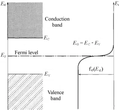
where EF is the Fermi energy representing the energy at which the Fermi distribution fe EF =1/2 and k is the Boltzmann constant. The Fermi distribution is drawn in Figure 1.15
for illustration.
Figure 1.15: The energy bands together with the Fermi distribution function. The Fermi level EF is
defined such that fe Ee =1/2 if Ee = EF.75
Therefore, the density of electrons in the conduction band is calculated as: 3
ne= σωexp −EωkT− EF (1.14) with σω = β βπme *kT hβ γ/β (1.15)