HAL Id: hal-03187813
https://hal.archives-ouvertes.fr/hal-03187813
Submitted on 1 Apr 2021HAL is a multi-disciplinary open access
archive for the deposit and dissemination of sci-entific research documents, whether they are pub-lished or not. The documents may come from teaching and research institutions in France or abroad, or from public or private research centers.
L’archive ouverte pluridisciplinaire HAL, est destinée au dépôt et à la diffusion de documents scientifiques de niveau recherche, publiés ou non, émanant des établissements d’enseignement et de recherche français ou étrangers, des laboratoires publics ou privés.
Comparing analytical and Monte-Carlo-based simulation
methods for logic gates SET sensitivity evaluation
R Schvittz, Y Aguiar, Frédéric Wrobel, J-L Autran, L. Rosa, P Butzen
To cite this version:
R Schvittz, Y Aguiar, Frédéric Wrobel, J-L Autran, L. Rosa, et al.. Comparing analytical and Monte-Carlo-based simulation methods for logic gates SET sensitivity evaluation. Microelectronics Reliability, Elsevier, 2020, 114, �10.1016/j.microrel.2020.113871�. �hal-03187813�
Comparing Analytical and Monte-Carlo-based Simulation Methods for Logic
Gates SET Sensitivity Evaluation
R. B. Schvittz, Y. Q. Aguiar, F. Wrobel, J.-L. Autran, L. S. Da Rosa Jr., P. F. Butzen
Abstract –This paper presents a discussion related to two different methods used to evaluate logic gate susceptibility considering Single Event Transient faults at the layout level. These methods can be adopted into radiation-hardening-driven optimizations to improve the overall reliability of circuits. The results show that the simulation approach presents a higher accuracy by considering charge-sharing effects. At the same time, the analytical method can provide similar results in a faster manner.
1. Introduction Section 6 provides some final remarks. Single-Event Effects (SEE) can be defined as the result of
the interaction of highly energetic particles, such as protons, neutrons, alpha particles, or heavy ions, within the sensitive regions of a microelectronic device or circuit [1]. In particular, with the reduction of transistor dimensions, memories are more sensitive to Single-Event Upset (SEU) and combinational circuits are more subjected to Single-Event Transient (SET). SET is one of the most common faults in modern design, even for terrestrial applications [2]. The radiation-induced transient current can produce wrong output signals and provoke failure in the systems. The widely known redundancy techniques used to deal with SEEs, such as Triple-Modular Redundancy (TMR), usually impose overhead in area and power consumption [3]. To avoid the overdesign and guarantee the best option to the fabricated circuit, many reliability evaluation methods may be used. Radiation robustness can also be obtained through reliability-aware logic and physical synthesis in semi-custom designs based on standard-cell methodology [4]. In other words, it is possible to harden a circuit by selectively using logic gates that minimize the SET generation or propagation in the most vulnerable nodes of a complex VLSI design.
2. Background
Many advances in the integrated circuits are achieved due to technology scaling. The fabrication of even more capable computing architectures has been enabled by smaller, faster, and cheaper fundamental microelectronic building blocks. However, the voltage scaling associated with the fact that the amount of charge that represents stored information has dropped lower and lower, increasing the sensitivity of CMOS devices to single-particle charge collection transients. Also, the higher frequency achieved by the circuits can intensify the soft errors due to the reduction in the timing masking.
In the case of Single event transient (SET), it is caused by the generation of charge due to a single particle passing through a sensitive node in the combinational circuit. This strike in a sensitive node within a combinational logic circuit can produce a wrong output value during a time interval. The pulse generated by the particle strike can have a positive or negative magnitude, depending on whether the particle hits at the sensitive node of the NMOS or PMOS transistors.
The sensitive node in a circuit is the reverse-biased PN junctions [7]. When these particles hit the silicon bulk, the minority carriers are created, and if collected by the source/drain diffusion regions, the change of the voltage value of those nodes occurs [8].
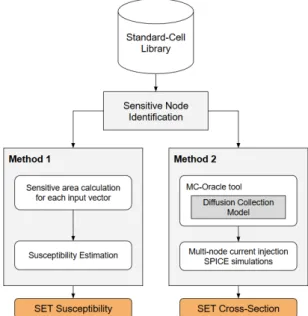
In this way, this work proposes a discussion of two different methods for logic gates susceptibility evaluation against SET faults at layout-level. The two methods are presented in the diagram in Fig. 1. The first method is an analytical method that evaluates the logic gates based on the sensitive area and particle flux [5]. The second one is a methodology used to calculate the charge collection process and the SET cross-section through Monte Carlo simulations. The discussion in this digest is based on the application of the two methods in 10 logic gates of 45nm FREEPDK standard cell library [6]. The selected gates are INV_X1, INV_X2, NAND2_X1, NAND2_X2, NOR2_X1, NOR2_X2, NAND4_X1, NOR4_X1, AOI21_X1, and OAI21_X1. The results are used to compare the efficiency of both methods evaluating the set of logic gates at layout-level.
In addition, considering the NAND2 gate as an example shown in Fig. 1, the output node G, which belongs to the transistor M1 is sensitive when the input vector DE=”10” is applied, albeit it is an ON-transistor. Furthermore, as the behavior of the SET faults is different for a PMOS/NMOS particle strike, it is assumptive that the main condition for reverse-biased PN junctions is satisfied on complementary OFF-plane of the gate, instead of in the OFF-transistors. Moreover, some internal nodes of a gate are not always sensitive to the particle strike. The pulse generated due to the particle strike in an internal node will not propagate if there is not a logical sensitized path to the output. Then, the pulse propagation from a sensitive node to the output depends on the state of the inputs [9]. Fig 2 shows an example of a sensitive node and pulse propagation in a NAND gate. When DE=”10” then there is a sensitive path between N3 and G, making N3 a sensitive node for this specific input vector. However, the input vector “11” also makes a sensitive path between N3 and G, This paper is organized as follows: Section 2 provides a
review on the foundation of reliability of circuits related to radiation effects; the two evaluation methods are presented in Section 3; the comparison evaluation methodology is proposed in Section 4; Section 5 presents the results for each method and discusses the differences between them; and, to conclude,
Final version is available at https://doi.org/10.1016/j.microrel.2020.113871
Cite this article as: R. B. Schvittz et al., "Comparing Analytical and Monte-Carlo-based Simulation Methods for Logic Gates SET Sensitivity Evaluation," in Microelectronics Reliability, vol. 114, November 2020, doi: 10.1016/j.microrel.2020.113871.
although, in this condition, the node is not reverse biased. sensitive active area, it is possible to determine the number of faults per hour (p) in a given logic gate input vector. This information is obtained through Eq. 1, where 𝜑 is the particle flow and defined in particles/nm²*h and Δ in nm². The analytical method can calculate the susceptibility of the logic gates by evaluating the constructed layout by merely applying the defined equation.
Fig. 1. Node sensitive analysis in a NAND gate (adapted from [9])
3. Methods for Sensitivity Evaluation
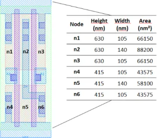
In this section, the two techniques for assessing the sensitivity of logic gate layouts in the presence of SET faults will be presented. Then an application example using a NAND2 logic gate is used to make the presentation of the methods more natural to understand. The layout of this gate and the corresponding active area sizes is presented in Fig. 2.
Fig. 3. Flowchart
𝑝 = ∆ ∗ 𝜑 (1)
As an example, consider the two-input NAND function presented in Fig. 3. The figure shows the size information of each active area of this gate. As can be observed, the nodes n1, n3, and n4 are connected to the VDD/GND terminals, and then they are not sensitive.
Considering input “00”, the only node in the reverse biased condition is the node n6, then, the total sensitive area in this input vector is the area of n6. The same behavior occurs considering input “01”, and the only sensitive node is n6. On the input “10”, the nodes n6 and n5 are sensitive because they are reverse biased, in this case, the total sensitive area is the sum of n5 and the n6 regions. In the last input vector, “11”, the sensitive area is on pull-up plane, and the only sensitive node is n2. The values calculated for this gate and its input vectors are presented in Table I.
Fig. 2. NAND2 layout and its respective nodes sizes
3.1. Analytical Method
The analytical method is based on the total sensitive area of the layout at each input vector and a particle flux. Based on the logic gate layout, the analytical method is able to assess each input vector's amount of sensitive area and thus determine, based on a particle flux, the number of failures that will occur per hour of operation. Fig. 3 shows the flowchart of the method.
TABLEI
SENSITIVE NODES FOR NAND2 AND THE CORRESPONDING SENSITIVE AREA
Input vector (A2A1)
Sensitive nodes
Total sensitive area (nm²)
00 n6 43575
01 n6 43575
The first step to determine the sensitive nodes in each input vector of a logic gate is to identify the expected output of this vector. From this information, it is possible to identify which plane of the gate is sensitive (pull-up or pull-down), which is performed in the next step. Then, with the necessary information obtained, the vulnerable nodes are identified, and the input vector's sensitive active area is calculated. The total of sensitive active area in each vector is known as Δ.
10 n5 and n6 101675
11 n2 88200
To exemplify the flowchart, we will use the particle flux defined in [10]. It is important to note that the analytical method has this information as input. It will work for any particle flux analyzed. With that, 𝜑 = 3.6*10-11 particles/nm²*h
is considered. Table II shows the final susceptibility results Finally, with the information obtained about the total
obtained for each input vector of the NAND2 logic gate.
TABLEII
SUSCEPTIBILITY CALCULATED FOR EACH INPUT VECTOR OF NAND2 GATE
Input vector (A2A1)
Total sensitive area
(nm²) p (10-6)
00 43575 1.57
01 43575 1.57
10 101675 3.66
11 88200 3.18
3.2. Simulation Method based on Monte-Carlo Approach
In the second method, a Monte-Carlo prediction methodology is adopted based on the MC-Oracle tool [11] for the particle interaction physics and SET cross-section calculation. The sensitive areas of each design are extracted from the GDS (Graphical Design System) file and the diffusion model rules the charge collection process. Different approaches can be used to identify the sensitive zones of each input vector. For the sake of comparison, the same sensitive node evaluation approach presented in the previous subsection is adopted here. The range and the electronic stopping power for each ion is calculated using the SRIM (Stopping and Range of Ions in Matter) tool [12] and used in the ionization process inside of the MC-Oracle calculations. Once the energy deposition is calculated for each particle strike in the circuit layout, the charge collection calculation is performed following the drift-diffusion model [11]. As output, the MC-Oracle tool provides a SET database containing all the transient currents observed for each electrode of the circuit. This database is used to perform the current injection through SPICE electrical simulations.
Fig. 4. Diagram of the two analyzed methods
In the analytical method, it is considered that a particle incidence on a sensitive node has sufficient energy to cause a voltage change. For the inputs of the gates, the same signal probability, i.e. the probability of the signal to be at high logic level of 50% was used. To perform the analysis using the analytical method, we considered a particle flux equal to 3.6*10-11particles/nm²*h. Regarding this value, the authors
reiterate that this is an input of the method, being possible the evaluation considering any particle flux. For the simulation method, it was considered particle LET of 78.23 MeV-cm2/mg.
The results presented are the mean susceptibility (analytical method) and cross-section (simulation method) obtained for each logic function. The comparison between the methods will assess the ability to identify and evaluate the logic gates that are more sensitive to transient failures. In addition, the ability to identify the most sensitive vector and the behavior of the other input vectors of the logic gates will be assessed.
Due to a SPICE-based multi-node current injection, this method is able to assess the charge sharing effect between adjacent sensitive nodes. For a given Linear Energy Transfer (LET), i.e. the amount of energy lost by a particle per unit length, tens of thousands of particle events are simulated to obtain a minimum of 100 observed SET events. More information about this prediction methodology can be found in [13].
5. Results (3 colunas) 4. Evaluation Methodology
In this section, the results obtained by the methods discussed in this work will be presented, considering the logic gates previously defined. The results will be divided considering each method, and afterward, a discussion with more details about the origins of the differences obtained between them is carried out.
This section presents the methodology for evaluating the methods used in this work. Ten logic functions are analyzed to compare each technique's efficiency in assessing the sensitivity of the layouts in the presence of transient faults. These gates are INV_X1, INV_X2, NAND2_X1, NAND2_X2, NOR2_X1, NOR2_X2, NAND4, NOR4, AOI21, and OAI21. The operation flow of the function evaluation methodology is shown in Fig. 4. The standard cells are evaluated in terms of susceptibility and cross-section by each method.
5.1. Analytical Method Results
The results of applying the analytical method to the analyzed logic gates can be seen in Fig. 5. The results are based on the average susceptibility of each logic gate. Another important point is that gates which presents higher standard deviation values for susceptibility can be highly sensitive to pin assignment. This implies that minimum differences between input vectors probabilities could increase and/or decrease the susceptibility calculated for these gates. Among the logic gates analyzed, it can be highlighted that the AOI21 function had the highest average susceptibility. Another critical point to note is that gates with higher driving capacity are more susceptible than the minimum sizing version. This behavior is justified by the increase in the size of sensitive active areas.
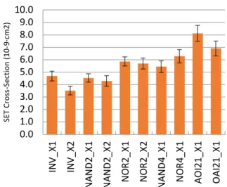
Fig. 6. Results for cross-section of the logic gates analyzed in this paper
5.3. Discussion
We made a comparison between the two methods covered in this work. In this way we can list possible pros and cons between them. The first method, the analytical one, has as its main advantage its ability to evaluate the logic gates quickly. However, for not considering the electrical conduction characteristics of the logic gates, it suffers from a lack of accuracy. The second method, however, has as its main advantage its accuracy in the analysis, also considering the charge sharing between the PN junctions. However, the evaluation of logic gates requires a large number of electrical simulations, leading to a very time-consuming process.
To better illustrate our analysis, we will consider the inverter logic gate as an example. To highlight the source of these differences between the two methods, consider this gate with two different driving strengths (X1 and X2). Hence, an analysis by the input vector of this gate is presented in Fig. 7. In the same way, as mentioned earlier, both methods can identify the most sensitive vector of the logic gates.
Fig. 5. Results for susceptibility of the logic gates analyzed in this paper
5.2. Simulation Method Results
The results of applying the simulation method to the analyzed logic gates can be seen in Fig. 6. The results are based on the cross-section of each logic gate. In the same way as in the method previously discussed, the AOI21 logic function was the one with the highest cross-section value. Also, when comparing the NAND and NOR gates, the same observations can be done: NAND2_X1, NAND2_X2 and NAND4_X1 are less sensitive than the NOR2_X1, NOR2_X2, and NOR4_X1, respectively. However, when comparing all the cells considering the most sensitive to the most robust, provided by both methods, some divergences can be found. In the next subsection, the possible sources of these differences will be discussed.
As the analytical method considers only the sensitive area, by increasing the gate's ability to conduct, the sensitive area is also increased. Thus, the analytical method ends up considering the INV_X2 gate as more susceptible. It is correct because more particles tend to collide in this region by increasing the size of the active area, increasing the susceptibility. However, at the same time that more particles fall into this increased active area, the higher drive strength requires more charge collection to cause an observable fault in the output of the circuit, leading to an increase in the minimum collected charge 𝐶𝐶!"# (also known as critical charge, 𝑄$%"&). This can be
observed in the cross-sections in Fig. 7, which the INV_X2 showed a lower SET cross-section when compared to the INV_X1. It means that the increase in the 𝐶𝐶!"# dominates
over the impact of increasing the active area. Thus, but only considering the increase in area and disregarding the importance of the circuit driving capability and nodal 0.0 1.0 2.0 3.0 4.0 5.0 6.0 7.0 8.0 9.0 In v_ X1 In v_ X2 NA ND 2_ X1 NA ND 2_ X2 NO R2 _X 1 NO R2 _X 2 NA ND 4_ X1 NO R4 _X 1 AO I2 1_ X1 OA I2 1_ X1 Su sc ep tib ili ty (10 -6 par tic le s/ nm ²*h ) 0.0 1.0 2.0 3.0 4.0 5.0 6.0 7.0 8.0 9.0 10.0 IN V_ X1 IN V_ X2 NA ND 2_ X1 NA ND 2_ X2 NO R2 _X 1 NO R2 _X 2 NA ND 4_ X1 NO R4 _X 1 AO I2 1_ X1 OA I2 1_ X1 SET Cr os s-Se ct io n (10 -9· cm 2)
capacitance can lead to miscalculation of the overall sensitive
of the circuit. NOR2_X1 are highlighted along the probability density function of the charge collection distribution. From the
Fig. 7. Results for susceptibility and cross-section of INV_X1 and INV_X2 logic gates
Similarly to what observed for the inverter, both methods were able to identify the same critical vector in the NOR2 logic gate, as shown in Fig. 8. As observed for the inverter gate, the analytical method has shown an increased susceptibility for all input vectors in the NOR2_X2. As the analytical method disregard the electrical characteristic in the susceptibility analysis, all vectors have an increase in this value comparing X1 with X2. However, an interesting fact about this logic gate is observed in the input vector 00. When increasing the conduction capacity of the gate from X1 to X2, it showed an increase in both methods, the susceptibility and the SET cross-section. One possible explanation would be that, as the active area of the sensitive transistor for this input has its size doubled, the larger sensitive area effect dominates the radiation
response of the circuit. thousands of particle event simulations and charge collection calculation, only the events that lead to an observed SET in the output of the gate are considered in this analysis.
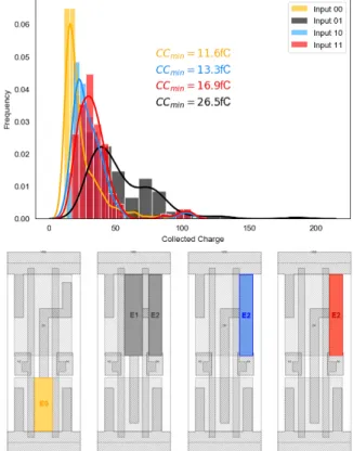
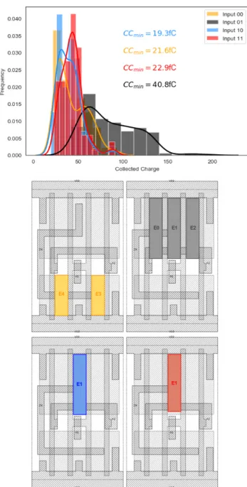
Firstly, it can be easily noticed the difference in the CC distribution for each input vector, justifying the input dependence observed in the SET cross-section in Fig. 8. The input vector which has shown the lowest 𝐶𝐶!"# is the 00 and
10, about 11fC and 13fC, respectively. Similarly, this two input combination presents the highest SET cross-section. Now, considering the increased driving strength gate, the NOR2_X2, the results are shown in Fig. 10. The same input vectors presents the lowest the lowest 𝐶𝐶!"#. However, a wider CC
distribution is observed for all inputs due to the larger sensitive area, about 80% increase in the total drain collecting area. The sensitive area for the input 10 and 11 has shown the lowest increase, about 33%. The most increased area was observed for the input 00, in 100%, i.e. the area is duplicated. Although, it is also possible to see an increase in the 𝐶𝐶!"#, from 11fC to
21fC, the increase in area still dominates the overall response of the circuit leading to an increase in the SET cross-section. Thus, for the circuits and input scenarios in which the drain collecting area dominates the overall sensitivity of the circuit, the analytical can provide a better accuracy.
Fig. 8. Results for susceptibility and cross-section of NOR2_X1 and NOR2_X2 logic gates
However, all input combinations have its sensitive transistors upsized and, consequently, the sensitive area increased. To better understand why only the input vector 00 has shown an increase in the SET cross-section for the NOR2_X2, an analysis of the collected charge must be taken into account. For that, the results obtained from the Monte Carlo simulation approach should be used. In Fig. 9, the sensitive areas corresponding to each input vector of the
Both methods presented in this work seek to measure the sensitivity of circuit layouts in the presence of radiation effects. However, it was seen that the analytical method, although it 0.0 1.0 2.0 3.0 4.0 0 1 Su sc ep tib ili ty (10 -6) INV_X1 INV_X2 0.0 2.0 4.0 6.0 0 1 Cr os s-sect io n (1 0-9) INV_X1 INV_X2 0.0 2.0 4.0 6.0 8.0 10.0 00 01 10 11 Su sc ep tib ili ty (1 0-6) NOR2_X1 NOR2_X2 0.0 2.0 4.0 6.0 8.0 10.0 00 01 10 11 Cr os s-se cti on (1 0-9) NOR2_X1 NOR2_X2
Fig. 9. Sensitive areas for each input vector and the probability density function of the collected charge for the NOR2_X1.
manages to identify the most sensitive vector of the logic gates, 6. Final Remarks
In this work, we discuss the importance to fast and accurately evaluate the circuit susceptibility to radiation effects. We evaluated two methods to assess the sensitivity to SET in logic gates considering the layout-level. Both methods have their advantages and disadvantages presented. The complete analysis proposed in this work provides a relevant set of information to design reliable circuits to radiation environments. Given the complexity of both methods, a new one, which can unite the strengths of each technique shown here, is necessary to evaluate the logic gates more efficiently and accurately. It would need to be quick and effective in the evaluation and could be easily adapted in the project flow of the library cells. In this way, it is intended in future works to add the logic gates' electrical information based on the size of the active areas in search of a better evaluation carried out by the analytical method.
References
[1] Munteanu, D., and J-L. Autran. "Modeling and simulation of single-event effects in digital devices and ICs." IEEE Transactions on Nuclear science 55.4 (2008): 1854-1878.
[2] V. Ferlet-Cavrois et al., “Single Event Transients in Digital CMOS – A Review”. IEEE Trans. Nucl. Sci. 60 (2013): 1767-1790. [3] J. Vial, A. et. al, “Using tmr architectures for yield improvement,”
DFT, 2008, pp. 7–15.
[4] Y. Q. Aguiar et al., “Radiation hardening efficiency of gate sizing and transistor stacking based on Standard Cells,” Microelectron.
Reliab. 100-101 (2019).
[5] Schvittz, R, Leomar S., and Paulo F. B. "Exploring Logic Gates Layout to Improve the Accuracy of Circuit Reliability Estimation." 2019 VLSI-SoC, 2019.
[6] NanGate FreePDK45 Generic Open Cell Library. Retrieved from http://projects.si2.org/openeda.si2.org/projects/nangatelib. [7] Baumann, R. C. “Radiation-induced soft errors in advanced
semiconductor technologies”. IEEE Trans. on Device and materials reliability, v. 5, n. 3, p. 305-316, 2005.
[8] Omana, M., et al. "A model for transient fault propagation in combinatorial logic." IOLTS 2003.
[9] Gill, B. S., et al. "Node sensitivity analysis for soft errors in CMOS logic." ITC, 2005.
[10] Normand, E. ”Single event effects in avionics and on the ground”. In: Radiation Effects And Soft Errors In Integrated Circuits And Electronic Devices. WorldScientific, 2004. p.1–14. [11] Wrobel, F., and Frédéric S. "MC-ORACLE: A tool for predicting
soft error rate." Com. Phy. Communic. 182.2 (2011): 317-321.
fails to evaluate considering the electrical characteristics, and this ends up omitting some information in the analysis. The simulation method, on the other hand, unlike the analytical method, this, in turn, manages to evaluate in more detail the logic gates considering their electrical characteristics. On the other hand, the limitation in using this method occurs precisely in the time necessary to evaluate the logic gates. The time required to evaluate the logic gates makes it impossible to use it in conjunction with a layout generator for functions with more than three inputs, for example.
[12] J.F. Ziegler., The Stopping and Range of Ions in Solids, Pergamon, New York, 1985, http://www.srim.org/
[13] Y. Q. Aguiar et al., “Mitigation and Predictive Assessment of SET Immunity of Digital Logic Circuits for Space Missions,”
Aerospace (2020): 1-12.
Fig. 10. Sensitive areas for each input vector and the probability density function of the collected charge for the NOR2_X2.
E4 E1 E1 E1 E3 E2 E0