Design of a Very High Frequency dc-dc
Boost Converter
by
Anthony Sagneri
B.S., Rensselaer Polytechnic Institute (1999)
Submitted to the Department of Electrical Engineering and Computer
Science
in partial fulfillment of the requirements for the degree of
Master of Science
at the
MASSACHUSETTS INSTITUTE OF TECHNOLOGY
February 2007
@
Massachusetts Institute of Technology, MMVII. All rights reserved.
Department oilectricai Engineering
/1
and Computer Science February 2, 2007 Certified by Accepted by MASSACH
7
ETT(I INSTITUTE COF TE iKNOLOGY TUTE GyE
APR el o
R
t2007
STP
LIS 1;
LISpjkRIES
David J. Perreault ssoci e o fE ctri Ergineering es upervisorArthur C. Smith Chairman, Department Committee on Graduate Students
Design of a Very High Frequency dc-dc Boost Converter
by
Anthony Sagneri
Submitted to the Department of Electrical Engineering and Computer Science on February 2, 2007, in partial fulfillment of the
requirements for the degree of Master of Science
Abstract
Passive component volume is a perennial concern in power conversion. With new circuit architectures operating at extreme high frequencies it becomes possible to miniaturize the passive components needed for a power converter, and to achieve dramatic improvements in converter transient performance. This thesis focuses on the development of a Very High Frequency (VHF, 30 - 300 MHz) dc-dc boost converter using a MOSFET fabricated from a typical power process.
Modeling and design studies reveal the possibility of building VHF dc-dc converters operable over the full automotive input voltage range (8 - 18 V) with transistors in a 50 V power process, through use of newly-developed resonant circuit topologies designed to minimize transistor voltage stress. Based on this, a study of the design of automotive boost converters was undertaken (e.g., for LED headlamp drivers at output voltages in the range of 22 - 33 V.)
Two VHF boost converter prototypes using a <b2 resonant boost topology were de-veloped. The first design used an off the shelf RF power MOSFET, while the second uses a MOSFET fabricated in a BCD process with no special modifications. Soft switching and soft gating of the devices are employed to achieve efficient operation at a switching frequencies of 75 MHz in the first case and 50 MHz in the latter. In the 75 MHz case, efficiency ranges to 82%. The 50 MHz converter, has efficiencies in the high 70% range. Of note is low energy storage requirement of this topology. In the case of the 50 MHz converter, in particular, the largest inductor is 56 nH. Finally, closed-loop control is implemented and an evaluation of the transient characteristics
reveals excellent performance.
Thesis Supervisor: David J. Perreault
Acknowledgements
My thanks are due to the National Science Foundation, National Semiconductor, and the MIT EECS department for sponsorship. To Prof. Dave Perreault, my research advisor, and tacit instructor in all things power electronics, who somehow always seems to stay grounded. To Juan Rivas, also a tremendous source of knowledge, and emissary of laboratory shenanigans along with Jackie Hu and Grace who help to keep the atmosphere light. To Draper Dave, whose ability to warp space-time with his mere presence very nearly caused me to miss yet another degree cycle. To Olivia, Yehui, and Robert who have been helpful at various times over the course of things (and John Ranson who measured some stuff for me), and Brandon Pierquet, without whom I probably never would have found LEES. The rest of LEES also has my thanks, including the giant cockroaches and sewer rats in 10-082, for making things what they are.
I can't help but acknowledge the USAF (United States Air Force or you non-separated military folk), as I probably wouldn't be here if it weren't for the collusion of a whole lot of things that happened there. My fellow MSI cadre: Jeff Painter (also a groomsman, thanks!), Lupe Sabala, Gary Ayers, Dee Melendez, and even Dean, who shared many thrashings, triumphs, and curse words (like, "those !bleeps! at INYR"). It's doubtful I would be here if I didn't have you guys as a team to make me look good to the admissions folks. I still think that Hanscom SRGH should report to MGH for a cleaning. Is 10.2 up and running yet?
Of course, all my friends from other places who have helped me over the years deserve explicit thanks: Lester Pangilinan, my best man, Abe Chayya (charlie india), Manger, Christie, Deano Busch, George, Monica, Matt, Bill, Jess, Jerry Wilson, everyone who is married to one of these people, unless I don't know you, and everybody I forgot.. .you know who you are.
To Wendy, my wife, who has been a great help when I need distraction, I love you. Thanks!
To Mom and Dad who managed (by dumb luck!) to bring me into the world, and then (not by dumb luck) helped me find my way all the way here (which is about 4.5 hours from where I started). Thanks! Oh, and to my brothers and sisters, who have been useful at times.
-5-Contents
1 Introduction
1.1 Losses in hard switched converters . . . . 1.2 Resonant Power Conversion . . . . 1.3 Contributions and Organization of the Thesis . . . .
2 The 12 Inverter
2.1 The class 1 Inverter . . . .
2.2 The class 42 Inverter . . . . 2.2.1 Basic Operating Principles . . . .
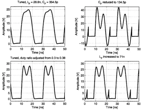
2.2.2 Tuning the D2 Inverter . . . .
2.2.3 Nonlinear Capacitance Effects on the
3 The 3.1 3.2 4b2 Inverter (D2 dc-dc Converter A Resonant Rectifier . . . . The Power Stage . . . . 3.2.1 Important Device Characteristics 3.2.2 Linking the Inverter and Rectifier
4 Converter Prototypes
4.1 The First Prototype . . . . 4.2 A Second Prototype . . . . 17 18 24 27 31 31 35 37 43 57 59 60 67 68 72 79 79 89
-7-5 Closed-Loop Operation 5.1 Control Scheme . . . . . 5.2 A Resonant Gate Drive . 5.3 The Controller . . . . . 5.4 Closing the Loop . . . .
6 Conclusion
6.1 Thesis Summary . . . . 6.2 Thesis Conclusions . . . 6.3 Future Work . . . .
A SPICE DECKS AND COMPONENT A.1 Chapter 1 Data ...
A.1.1 Fig. 1.4 data: ... A.2 Chapter 2 Data ...
A.2.1 Fig. 2.3 data: ... A.2.2 Fig. 2.4 data: ... A.2.3 Fig. 2.7 data: ... A.2.4 Fig. 2.11 data: ... A.2.5 Fig. 2.13 data: ... A.2.6 Fig. 2.14 data: ... A.2.7 Fig. 2.15 data: ... A.2.8 Fig. 2.17 data: ... A.2.9 Fig. 2.19 data: ... A.3 Chapter 3 Data ...
A.3.1 Fig. 3.4 data: ... A.3.2 Fig. 3.5 data: ...
A.3.3 Fig. 3.6 data: . . . .
VALUES 99 99 101 106 108 115 115 116 117 119 119 119 121 121 122 123 124 126 128 129 132 134 136 136 137 138
Contents
A.4 Chapter 4 Data . . . 139
A.4.1 ST Converter Final Spice Deck . . . 139
A.4.2 50MHz Converter Final Spice Deck . . . . 145
A.4.3 SPICE Model Libraries . . . . 151
B PCB Layout Masks and Schematics 159
Bibliography 167
-9-. -9-. -9-. 19
. . . 20
1.1 Synchronous Buck Converter Active vs. Passive Volume . . . . . 1.2 Buck-Boost Converter Illustrating Energy Storage Requirements 1.3 MOSFET Model . . . . 1.4 Class E Inverter Performance vs. Load Resistance . . . . 1.5 VHF Converter Under On-Off Modulation . . . . 22 25 26 Shorted quarter-wave line . . . . Half-wave symmetry/repetition . . . . Class-4 Inverter and waveforms . . . . 4D Waveforms when inverter is purposefully detuned The (2 Input network and its bode plot . . . . The )2 Inverter . . . . 4D2 Inverter waveforms . . . . 4b2 and transmission line responses . . . . Block diagram of source substitution method . . . . 4D2 inverter split for harmonic balance analysis . . . (2 network response to initial conditions . . . . Duty ratio vs. harmonic composition . . . . (D2 drain-source impedance effects on drain voltage Tuning sequence to increase peakiness . . . . Tuning characteristic impedance . . . . Controlling power in (2 inverter . . . . Loss vs. tuning in D2 . . . . .. . . . . . . . . . . 32 . . . . 33 . . . . 34 . . . . 35 . . . . 36 . . . . 37 . . . . 38 . . . . 39 . . . . 40 . . . . 40 . . . . 42 . . . . 44 . . . . 47 . . . . 48 . . . . 49 . . . . 50 . . . . 52 2.1 2.2 2.3 2.4 2.5 2.6 2.7 2.8 2.9 2.10 2.11 2.12 2.13 2.14 2.15 2.16 2.17
List of Figures
2.18 Efficiency vs. tuning in (2 . . . .
2.19 Tuning vs. transient response . . . . 2.20 Efficiency vs. characteristic impedance 2.21 D2 inverter with nonlinear capacitance 3.1 Series-loaded resonant rectifier . . . . 3.2 D2 boost converter . . . . 3.3 Series-loaded resonant rectifier in SPICE 3.4 Rectifier waveforms . . . . 3.5 AC-DC power split in rectifier . . . . 3.6 Tuning rectifier by controlling Fc and ZO . 3.7 MOSFET parasitic mechanisms . . . . 3.8 3.9 3.10 3.11 3.12 3.13 3.14
Measurement Setup for RDS-ON vS. VGS and Temp Temperature dependence of MOSFET channel resis
Capacitance Measurement Setup . . . . Device capacitance models compared to measureme Rectifier waveforms . . . . Inverter and Converter Waveform Overlay . . . . Inverter and Converter Waveform Overlay . . . .
4.1 Ranking of devices based on class-E performance 4.2 42 converter schematic . . . . 4.3 Diode current ringing around CREC-diode loop 4.4 ST PD57060 42 converter simulation results . . . 4.5 Simulated and measured impedance match . . . .
4.6 ST PD57060 (2 converter measurements . . . . . 4.7 ST PD57060 (2 converter experimental waveforms latio n . . . . 4.8 50AJHz (2 converter simulation results . . . .
compared to simu-. simu-. simu-. simu-. simu-. simu-. simu-. simu-. simu-. simu-. simu-. 80 82 83 85 86 87 88 90 11 -. -. -. -. -. -. -. -. -. -. -. 53 . . . . 54 . . . . 56 . . . . 58 . . . . 60 . . . . 61 . . . . 62 . . . . 63 . . . . 64 . . . . 66 . . . . 68 erature . . . . 70 tance . . . . 71 . . . . 72 nt . . . . 73 . . . . 74 . . . . 75 . . . . 77
'tD2 schematic with component values for BCD process . . . .
Breakdown of important loss mechanisms for each prototype (simulated) 4.11 Experimental waveforms for the 50MHz converter
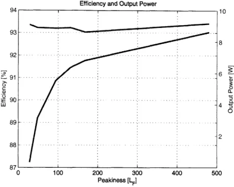
4.12 Experimental output power and efficiency . . . . 4.13 Converter photographs . . . . 5.1 5.2 5.3 5.4 5.5 5.6 5.7 5.8 5.9 5.10 5.11 5.12 5.13 5.14
VHF Converter Under On-Off Modulation . . Basic resonant gate drive . . . . Gate drive with shunt leg . . . . Final gate drive circuit . . . . Converter start-up transient . . . . Converter shut-down transient . . . . Converter efficiency vs. on-off modulation . . Gate drive power vs. output power . . . . Controller Schematic Diagram . . . . Closed Loop Operation . . . . Modulation frequency dependence on load and Schematic of load for load-step test . . . . Transient response to a load step . . . . Closed-loop efficiency measurements . . . .
VIN
B.1 Schematic of <D2 converter with ST part . . . . B.2 4D2 schematic with component values for BCD proces B.3 Complete gate drive schematic . . . . B.4 Complete controller schematic . . . . B.5 ST board layout masks . . . . B.6 ST board layout masks . . . . B.7 BCD board layout masks . . . . B.8 BCD board layout masks . . . .
. . . . 94 . . . . 95 . . . . 96 . . . . 100 . . . . 102 . . . 103 . . . . 104 . . . . 105 . . . 106 . . . 107 . . . . 108 . . . . 109 . . . . 110 S. . .. . . . 111 . . . .111 . . . . 112 . . . . 113 . . . . 159 s . . . . 160 . . . . 161 . . . . 162 . . . . 163 . . . . 164 . . . . 165 . . . . 166 4.9 4.10 91 92
13-3.1 Phase Shift differs for the ideal and non-ideal rectifiers when input bias voltage and amplitude are adjusted separately. Opposing effects of the junction capacitance cancel for the case when both bias voltage and amplitude are adjusted simultaneously. . . . . . 67 3.2 The components of the dc-dc converter examples are listed in this
table. More detailed information including the full spice models and values of parasitic inductances may be found in appendix A 76 4.1 M OSFET parameters . . . . 81 4.2 Faichild S310, 100V, 3A Schottky diode parameters . . . . 81 5.1 Hard gating requires more than twice as much power for the
cus-tom MOSFET even when the larger gate drive amplitude is ac-counted for . . . . . 102 B.1 Component values and part numbers for ST-based <D2 boost
con-verter . . . . 160 B.2 Component values and part numbers for Custom-MOSFET-based
<D2 boost converter . . . . 160 B.3 Component values and part numbers for gate drive circuit . . . . 161 B.4 Component values and part numbers for controller circuit . . . . 162
15-Chapter 1
Introduction
M
INIATURIZATION has become the pursuit of modern technology.Ubiquitous use of the term "nano-", while often cloying, underscores the importance at-tached to the search for the smaller. The integrated circuit stands as the benchmark to the nano-world, a stark example of how economic power can be harnessed through control of the tiny. While seedling ICs were analog circuits, the shrinking of digital systems occurred much more rapidly as a relentless march on Moore's law '. Today, a common theme in analog circuit design is the development of circuit topologies and techniques that allow the realization of traditional analog building blocks-op-amps, comparators, and the like-on the ever-shrinking CMOS processes. To the extent that more functionality can be realized by adding analog systems to a digital substrate or shrinking analog systems in general, there is money to be made. Take as an example the cellular telephone. The integration of the RF power amplifier along with a host of digital front-end signal processing has fueled the explosion of cell phone usage. While the goal is to have everything on a single chip realizing cost, reliability, performance, and functionality enhancements, some systems are challenging to integrate.
One particular area where integration remains largely a stymied endeavor is power conversion. Here, the issue centers around energy storage. Most switched mode power converters will use inductors and capacitors to fulfill the requirement. The amount of energy storage, and therefore the numerical values of the inductors and capacitors, is a function of the power processed, the switching frequency, and the details of the power processing scheme [1]. Typical converters like the boost or buck converter operating at a few tens of watts require too much energy storage to be integrated given current process constraints. While the statement may seem cavalier, consider that typical inductor and capacitor values for dc-dc converters on the scale of a few tens of watts
'Moore's law is mentioned only casually here. The fact is that analog circuits require fewer devices and benefit more from larger feature sizes and the better transistor parameters they engender. Digital circuits, however, rely on massive numbers of iterated structures that switch as rapidly as possible. The result has been an emphasis on shrinking the digital transistor to improve density.
-are measured in microhenries and microfarads, whereas integrated inductances and capacitances are more likely to be measured in nanohenries and picofarads. Assuming that three orders of magnitude in energy storage cannot be absorbed in an arbitrarily small volume, and that the techniques that are the subject matter of this thesis are not operating, the assertion is safe.
Typical inductors that might be realized on chip are in the range of a few 10s of nanohenries and capacitors in the 10s of picofarads. The main roadblock to achieving such small values with a conventional converter is loss. The balance of this thesis will explore converter designs intended to circumvent typical loss mechanisms in a manner compatible with integration and co-packaging.
1.1
Losses in hard switched converters
A switched mode power converter constructed of ideal elements has no intrinsic loss mechanism. Rather, they arise inevitably from the use of real components. These losses, distributed among the active and passive components constrain not only the efficiency of the SMPS (switched mode power supply), but the size, cost, form-factor, and even converter responsiveness. Finding ways to beat these losses is, in a sense, tantamount to miniaturization.
On considering a typical dc-dc converter, one fact that becomes obvious is that the bulk of the system, that is its weight and volume, comprises the passive energy storage elements. Semiconductor devices, having benefited from tremendous improvement since their inception, occupy only a small fraction of a typical converter footprint. This is made clear in figure 1.1 showing a common implementation of a synchronous buck converter where switches, gate drives, controller, startup and protection circuits, and the housekeeping power systems are integrated onto a die and placed in a QFN (quad flat-pack, no-lead) package. The remainder of the components are the energy storage devices which require roughly an additional four times the board area (not accounting for interconnect) and nearly six times the volume. It is not surprising, then, that techniques to reduce converter footprint might be aimed at minimizing or eliminating passive energy storage.
Where the goal is to reduce the size of the energy storage components, there are two primary ways to proceed. Either energy density may be increased or total converter
1.1 Losses in hard switched converters
'.S
2..2j
Figure 1.1: The synchronous buck converter components pictured will supply 7.5 W into 5 V. The QFN on the left encompasses the active switches, gate drive, control, and housekeeping functions. The remaining passive elements require 4 times the board area and 6 times the volume, not accounting for board interconnect.
energy storage reduced. Increasing the energy density implies shrinking a device for a constant amount of storage. Even if this can be accomplished, given the physi-cal constraints imposed by power dissipation, the increased losses that result often cannot be reconciled with good converter performance. Considering a solenoidal in-ductor, it is demonstrated in [2] that fundamental scaling between linear dimensions and flux- or current-carrying area causes inductor
Q to decrease as a
2 where a < 1 is a constant scaling each linear dimension. Similar relationships are enumerated in [3] for other geometries. In the case of capacitors, analogous problems arise. Where a given dielectric material is available, a lower bound exists on the capacitor plate separation for a set working voltage. Further, plate resistance also increases as plate thickness is decreased or plate area is increased, both are necessary to improve en-ergy density. These conditions imply that the capacitorQ will become unacceptably
low with continued scaling at a constant capacitance. Thus a host of factors -Q,
dielectric breakdown, and dissipation - impose a maximum energy density on pas-sive components. Unfortunately, practical densities leave something to be desired for converter size.With very limited leeway to increase energy density, we turn our attention to reducing the required energy storage. The classic solution is to raise the switching frequency
[1], thereby reducing the amount of energy processed per cycle, a condition that leads directly to smaller numerical values of inductance and capacitance. The flyback
-M1 D1
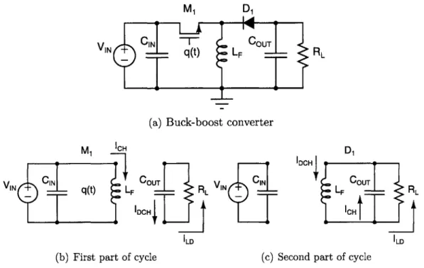
VI CI -T-- q(t) COUT
LF RL
(a) Buck-boost converter
M1 ICH D1
v
IN GOUTVTN
IF C77V1
IN + q(t) LF RL LF RL
T
IDCH DINCHtILD ILD
(b) First part of cycle (c) Second part of cycle
Figure 1.2: In the buck-boost converter, LF acts as temporary storage. In the first part of the cycle LF is charged by current ICH while COUT holds up the output. In the second portion of the cycle LF discharges into the load while replenishing COUT.
verter in figure 1.2 is a convenient means to an explanation. The buck-boost converter is an indirect converter. This type of converter transfers energy from the source to intermediate storage in the first portion of a cycle and then from intermediate stor-age to the load in the second portion of the cycle. The intermediate storstor-age in the flyback converter is the inductor, LF. As the switching frequency is increased and the amount of energy processed each cycle gets smaller, the numerical value LF can be reduced and the inductor made physically smaller for constant energy density. The same applies to the capacitors CIN and COUT. For instance, COUT must hold up the output voltage during the half of the cycle when LF is charging. The holdup time is inversely proportional to frequency as is the associated RC time constant for a constant droop in output voltage. Another way to see that COUT can be reduced is to consider that RL and COUT form a low-pass filter which attenuates the switching ripple. As the switching frequency increases the low-pass corner frequency moves up for a given attenuation, relaxing the capacitance requirement.
tech-1.1 Losses in hard switched converters
nique that may be used haphazardly: A cohort of loss mechanisms arise rapidly to place limits on the operating frequency. While not necessarily the largest of these, important frequency dependent losses in passive elements are limited almost exclu-sively to inductors and their magnetic materials. Most magnetic materials, used to increase inductance per unit volume, operate well at low frequency but have losses that rise rapidly otherwise. The basic trend is captured by the Steinmetz equation:
P,(t) = kf"Bl (1.1)
where P,(t) is the time-average loss per unit volume [kW/m2], B is the peak ac flux
amplitude [Gauss],
f
is the frequency of sinusoidal excitation [Hz], and the constantsk, a, and 13 are found by curve fitting. Examining 1.1 it is clear that for a greater
than one (it's often in the range of 1-3) that the loss will rise briskly with frequency. Another important implication is that the core volume may be increased to reduce the flux density, trading increased size for higher frequency-the opposite of the desired
effect2. In truth, the Steinmetz equation is only valid in a narrow range of situations, primarily where the excitation is sinusoidal and relatively low frequency. At high frequencies and under the non-sinusoidal excitation typical of power converters, the losses tend to be greater than predicted in the Steinmetz model and many different modeling approaches have been undertaken to get a more accurate prediction (for instance, [4]). The upshot, however, is that most bulk magnetic materials are not suitable for operation at frequencies much higher than a few megahertz.
One way of avoiding magnetic core losses is to do away with the magnetic core. The lower energy density demands even higher operating frequencies, but to the extent that the frequency can be increased, the magnetic loss picture looks much better. For a simple air core inductor, the inductance and resistance are determined primarily by geometry and the choice of conductor. Inductor quality factor
Q
is:wL
Q = (1.2)
R
In this simple relationship, expressing the ratio of energy stored to energy lost per
2Often loss becomes the limiting factor at high frequency and flux derating is necessary to avoid
excessive heat build up. Thus at high frequency cored inductors can actually get larger.
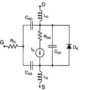
-D CGD LD RDS G RG KDB ID CDsALD CGS Ls S
Figure 1.3: A MOSFET including parasitic elements usually important in hard
switched dc-dc converter design
cycle,
Q
increases with reactance and decreases with resistance. The frequency depen-dence of R and L are very difficult to calculate for any geometry other than isolated straight wires. In general, skin effect, proximity effect, and interwinding capacitance affect both L and R [3]. If the proximity effect and the interwinding capacitance are ignored, the skin effect results in approximately a square-root increase in resistance with frequency. Since reactance rises linearly under these assumptions, thenQ
will increase ocVf.
Measurements of inductorQ
and information available from manu-facturers of air-core RF inductors indeed show thatQ
increases with frequency as a general trend.The seemingly synergistic effect of increasing
Q
with frequency for air-core inductors is only advantageous provided that the other frequency dependent loss factors are dealt with. These losses are associated with active semiconductor devices. Semiconductor losses can be divided into three main mechanisms for MOSFETs: conduction loss, switching loss, and gating loss. A MOSFET model including the parasitic elements usually considered in dc-dc converter design is shown in fig. 1.3.Conduction loss, due to the effective resistance of the channel, the lightly doped drain region (LDD), and metal/bondwire resistance, is only slightly frequency de-pendent3. Switching loss, however, depends significantly on frequency. It is helpful
1.1 Losses in hard switched converters
to further divide switching loss into overlap loss and losses resulting from discharge of the drain-source capacitance, CDS. Overlap loss refers to the condition where the MOSFET supports simultaneous voltage and current at its drain-source port and thereby dissipates power. This condition arises from the need to charge or discharge the device channel through finite source impedance (whether this impedance arises externally or as a result of device parasitic resistance and inductance) which imposes a minimum on switch transition times. Simplified models of overlap loss parameter-ized in converter nominal voltage (Vo) and current (Io), and MOSFET rise (Tr) and fall (T) times are readily available [5, 1]:
Er + Ef = kVoIo(Tr + Tf) (1.3)
The constant k reflects the circuit in which the device is used and varies between 1/6 and 1/2 depending on whether the load is purely resistive or clamped inductive. Since this result is basically fixed once the device and circuit are chosen, the energy per transition (E.
+
Ef) is also fixed. Therefore, as switching frequency rises, so doesoverlap loss.
The loss due to CDS occurs at device turn on, when the energy stored on the output capacitance is dumped into the switch yielding a loss than can be roughly approxi-mated as: 2CDSVGATE-PKf. This effect can be significant even at frequencies well
below a megahertz-CDS is usually fully charged just before turn-off.
Gating loss results from charging and discharging the input capacitance, CISS =
CGS + CGD. Calculating the gating loss is somewhat complicated by the presence of
CGD which is multiplied according to the Miller effect during transitions. In lateral
MOSFETs where CGD tends to be very small and its effects can be ignored, the gating loss is approximately expressed as:
PGATE = CGSVGATE-PKf (1.4)
This reflects that the loss is associated with the loss of charging a capacitor from a dc voltage through a resistor, ICV 2, and the subsequent dumping of the stored energy
channel and LDD components of RDS-ON are constant. Bondwire resistance is usually a small enough component that skin effect only accounts for a small change in the total
once per cycle. In other types of MOSFETs, such as vertical DMOS and even some lateral devices, CGD is a significant portion of CIss and the effects can't be ignored.
Then the gate power is usually expressed in terms of the total charge required per cycle to enhance the device:
PGATE = QGVGATEPKf (1.5)
In both cases the frequency dependence is clearly linear. This mechanism becomes important at switching frequencies of a few megahertz and beyond where gating loss for typical devices can range from hundreds of milliwatts to several watts.
Diodes also account for a fraction of the converter loss budget. All diodes have an associated forward voltage drop, VF, that combines with the forward current, IF, and resistive losses in the bulk regions to result in diode conduction loss. This mechanism is not explicitly frequency dependent. PN-junction diodes and PIN diodes, however, do have a frequency dependent loss mechanism - reverse recovery. Reverse recovery names the process in which stored minority carriers are removed during commutation. During the reverse recovery time, TRR, the carriers are extracted across a constant
voltage. Since this time is related to the amount of stored charge and the impedance of the external circuit, TRR is fixed for a given configuration. Therefore, the
en-ergy wasted per cycle to reverse recovery is constant implying frequency dependence. Schottky diodes, which are formed as metal-semiconductor junctions are majority carrier devices. They do not suffer heavily from reverse recovery losses, but are only available with breakdown voltages below about 120 volts.
1.2
Resonant Power Conversion
Resonance, usually ascribed to systems with complex poles displaying oscillatory behavior, is of some significance in power conversion. In filtering, for example, it plays a role to develop large immitance in comparatively little volume4. Here we look at resonance as a means to push back converter loss mechanisms and realize operation 4Series and parallel resonant filters can be used to shunt or block ripple in power converters. It
was demonstrated in [6] that by using resonance, filter element volume could be reduced by better than a factor of three.
1.2 Resonant Power Conversion
LCHOKE LRES RES
VIN M1 C RL
(a) Class E inverter
Effect of Load Change on Class-E Converter Waveforms and Efficiency
62 0 .. ... ... ... .... .. ... ... .. .. . 4 0 -... . -. --... ... . . 0- . .. 0 - -.-.-.-0 5 10 15 20 25 30 35 Time [ns] 100 90. -.- .-.- .- -a 80 ... ... ... ... .... .. ... w 70... ... ... ... 60-2 3 4 5 6 7 8 9 10 Load Resistance [9]
(b) 50 MHz Class E drain voltage waveforms
Figure 1.4: Resonant topologies often suffer from limited load range in power
conversion applications. Here, the Class E inverter waveforms are pictured as
the load is varied from
}R
to 2R. The properly tuned waveform is displayed in heavy black. The loss of ZVS and negative impact on efficiency are evident.in the very high frequency regime (VHF, 30 MHz - 300 MHz).
A number of converter topologies exist that draw from RF amplifier techniques to achieve efficient energy conversion [7, 8, 9, 10, 11, 12, 13, 14, 15] at high frequencies. These designs rely on reactive networks to shape the switch voltage and current and reduce switching loss. The class E converter, fig. 1.4(a), is a widely practiced topology whose network enforces a zero-voltage switching (ZVS) opportunity at turn-on. Its basic operation can be classified as indirect. The inductor LCHOKE is an open at the switching frequency, ensuring that only dc current flows from the source. With no dc path to the load energy from the source must first be stored on the switch shunt
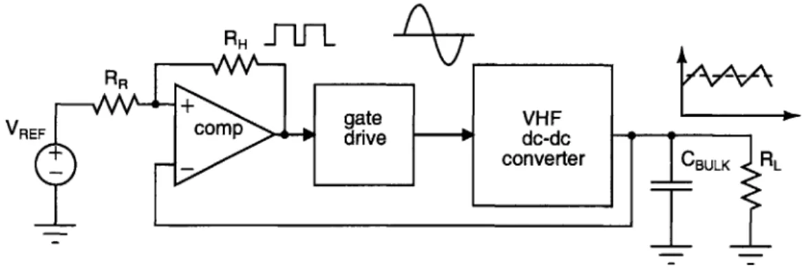
-RH _ _
RR
VRE + ompgate VHF
VREFC~mpdrive dc-dc
converter CBULK RL
Figure 1.5: Schematic depiction of VHF converter under on-off modulation. The closed-loop system keeps output voltage constant allowing the converter to deliver a constant power (effectively it sees a constant load) at it's most efficient point. Actual power delivered to the load depends on the duty ratio of the control signal.
capacitor Cp. The energy stored in Cp then rings towards the load in a cycle that is determined by the switching function, q(t), and the resonant tank formed by the load, LRES, and CRES- It functions by ringing the energy on CDS to the load once per
cycle. When these components are tuned according to [7, 8], the drain voltage will
naturally return to zero as the energy in Cp rings toward the load. At this point, the switch may be turned on with minimal loss. This mode of operation avoids the losses usually ascribed to the switch drain-source capacitance and largely avoids overlap loss, as well.
In practice, the drawbacks of such resonant topologies have prevented them from seeing widespread use. To begin with, the load range is severely restricted when compared with the 100:1 or better range achievable with conventional converters.
Resonating losses from circulating reactive currents become significant as the load
is reduced, hurting efficiency. The situation is made worse in the many cases where the load is an integral part of the resonance. Then, any change in load disrupts the ZVS condition and switching loss inevitably arises. This situation is depicted in fig. 1.4(b). Further difficulty arises because duty ratio control is often not possible. Instead, control is achieved by varying the switching frequency. The resulting poor
dynamics worsen with frequency and place an artificial upper bound on practically
achievable switching speed. Many resonant converters also suffer from high peak
switch stresses. The class E converter, in particular, has peak drain voltages rising
as high as 4.4 times the dc input voltage [16]. This is particularly troublesome where
1.3 Contributions and Organization of the Thesis
voltages.
Several of these issues can be resolved by partitioning the energy storage and control functions [17, 18, 191. Instead of controlling the output by varying the switching frequency, on-off modulation of the converter determines the fraction of output power delivered (see fig. 1.5). When the converter is on, it delivers a fixed power maintaining ZVS and maximum efficiency. When off, no power is delivered and there are no associated resonating losses. Under these conditions, the load range is a function of the minimum achievable modulation index. Such operation allows the network to be tuned to enforce ZVS at one particular operating point. The result is maximum efficiency, better dynamics, and higher achievable operating frequency. The fact that this mode of operation allows much higher switching frequency is self-reinforcing-high frequency means less energy storage so the converter can be started and stopped more rapidly and achieve a wider load range.
1.3
Contributions and Organization of the Thesis
Raising the switching frequency is a well known means of reducing required energy storage in power converters. It is precisely this reduction that can put inductor and capacitor values into the range that they might be considered for integration. For inductors, in particular, VHF operation allows magnetic materials to be set aside, avoiding the difficulty and expense of incorporating them on chip. Even so, it is not clear that current techniques, like the planar spiral inductor, can offer high enough
Q
or reasonable area. Generally, integrated inductors achieve Q's of ten or below with inductance in the neighborhood of 10-20 nH [20, 21]. While the techniques discussed in this thesis result in small value inductors, theQ
needs to be at least 50 or so. Capacitors are also a challenge. Typical CMOS processes achieve about 1 fF/Pm2 metal to metal capacitance. Higher density requires the use of inherently non-linear(and potentially lossy) gate capacitance. Yet these considerations are secondary to the question of whether or not devices available on the existing power processes are suitable to high frequency operation. The exploration and development of techniques that permit this answer to be "yes" is the primary contribution of this thesis.
Breakdown voltage is a key aspect in determining integrated process suitability. While adopting resonant circuit techniques permits low loss and high frequency it also poses very high switch stresses. The class E converter, for instance has an idealized peak
-voltage stress of 3.6 ranging up to 4.4 in practice. Since integrated processes do not enjoy the luxury of high breakdown voltage, attempting to implement a topology like the class E would significantly limit the input voltage range. Some RF amplifiers like the class F are able to reduce the peak stress by waveshaping [22, 23, 24], but at the expense of relatively high component count. In chapter 2 a new inverter we call class (D2 is introduced along with a tuning method that permits low peak voltage stress. The low voltage stress achieved (2 in simulation, 2.4 in experiment) is critical to implementing a converter with an input voltage up to 18 V on a 50 V power process, which for instance is not possible with a class E topology. The D2 also has a low component count and eliminates the need for an RF choke. With the few inductors resonant and small, the (2 has excellent dynamics and makes a good candidate for integration.
Efficient rectification compatible with integration is introduced alongside the T2
dc-dc converter in chapter 3. Many resonant rectifier topologies exist for RF inverters [13, 25, 26, 27, 28]. The particular topology set forth here offers a low component count. When mated with the inverter the result is a resonant boost converter that transfers power at ac and dc. The dc portion varies with the boost ratio and is advan-tageous because it does not suffer resonating losses. Almost all the power delivered at ac is delivered at the fundamental, where the rectifier is tuned to appear resistive. Significantly, the rectifier tuning changes with the dc input voltage causing the output power to vary nearly linearly with input voltage. Though this complicates design, it offers an additional degree of freedom to tailor the desired converter behavior. Device characterization and selection are critical. At VHF frequencies, the parasitic components must be embraced rather than avoided. This is a key strength of the D2, which can absorb the switch output capacitance as part of the wave shaping network. Both the magnitudes and distribution of the parasitic capacitance, inductance, and resistance are important considerations. Chapter 3 also discusses these particular aspects, and lays out the techniques used in measuring and modeling them.
Chapter 4 presents the design and experimental results of two dc-dc converter power stages. The first converter uses an off-the-shelf power LDMOS normally used in RF power amplifiers. The other converter uses an LDMOS device fabricated in a conventional silicon power process. Comparisons between the converters are drawn that help illustrate the effects of different tuning choices at design time.
1.3 Contributions and Organization of the Thesis
regime the gate drive is not a trivial ancillary issue. Hard gating with a totem-pole driver is out of the question. Even ignoring direct path losses in such a circuit, hard gating loss is too high. For that reason a resonant design was employed. The two key factors for a gate drive in this architecture are efficiency and startup time. Resonant schemes will naturally benefit over hard gating where efficiency is considered because some portion of the gate energy is recovered each cycle. On the other hand, direct control of duty ratio and dynamic response are compromised. A topology and specific tuning techniques are discussed that attempt to find the best trade offs.
Closed loop performance is a prerequisite for having a converter, per se. In chapter 5 a voltage-mode hysteretic controller closes the loop. The hysteresis band determines the converter peak to peak voltage ripple. A bulk capacitance in conjunction with the load sets the modulation frequency limits. Dynamic performance is excellent as the bandwidth is determined not by the modulation frequency, but by the delay through the controller and the power stage dynamics both of which are much faster.
Resonant power conversion with the 412 resonant boost converter can be accomplished with transistors built from a standard power process. VHF frequencies keep energy storage at a minimum yielding small component values and excellent dynamic per-formance. This and a discussion of future directions for related work are presented in chapter 6, Conclusion.
-Chapter 2
The
(D2
Inverter
C
HAPTER 1 laid out the basic considerations for conversionat VHF switch-ing frequencies and the attendant miniaturization advantages. While resonant conversion techniques are compelling in this regard, several key aspects make them difficult to integrate. At the top of the list is peak switch voltage stress. In practical implementations of the class E converter, for instance, the main switch must endure peak voltages up to 4.4 times the input voltage. This alone is enough to break an integrated implementation. Designs like the class F converter use wave shaping tech-niques to reduce the switch stress, but the result is a large component count. Many such converters also suffer from the need for a bulk inductor to function as an rf choke at the input. This limits dynamic performance and poses yet another challenge to integration. While variants like the second harmonic class E converter avoid this problem, no topology yet presented offers the combination of low switch stress, low component count, and minimal energy storage. Such a converter does exist and it is called the <D2 converter.
2.1
The class
<P
Inverter
As an aid to our understanding of the (D2 inverter's operation, we briefly digress to examine its progenitor, the class 4b inverter [2, 24]. This inverter exploits the sym-metrizing properties of a shorted quarter-wave transmission line in order to realize efficient high frequency conversion. The impedance characteristic of such a line is plot-ted in fig. 2.1 where the poles appear at the odd integral multiples of the fundamental and zeros obtain at the even integral multiples. The symmetrizing properties are ex-posed naturally on considering the effect of driving the line with a finite-impedance voltage source periodic in the fundamental. High impedance at the odd harmonics blocks current, permitting the source to impress odd harmonic voltages without
-Shorted Quarter-wave Transmission Line Impedance, f =50MHz0 70 6 0 --. -. - -. -. .. . .. 50-.... - ... ... ... ... ... ... ... 40-- . ... .... ... ... ... ... -3 0 - . - . - - -. - -.- -. - - - - --- - . c 2 0 - - - .- - -- - -- - --- - - -- - - - -M. 30 .. . .. ... . .. . .. . ... . . . .. . . . . . . .. . . . , 2 0 . . ... .. .. . .. . . .. . . . .. . . . . . . . . . .. 1.... ... .. .. . . .. . .... . .. .. . . . .. .. . . . .. . . . .. . . . 10 - - --- - -.. .- - - -0 - - -- - - -90 60 30 0 a -30 -60 -90 50 100 150 200 250 300 350 400 450 500 550 600 - .-.-- --- - - - -.-- --- -. ... -. -" -- - ---.-- --- --.-.- ...-. --. .-- -. -. -. -. -. -. -.... ... ... ... . .. .. . ..I.. ..... . .. . .. .... . --- - .. .- -- -- - -.--.-- -- - - - - ---- _ 50 100 150 200 250 300 350 400 450 500 550 600 Frequency [MHz]
Figure 2.1: Impedance characteristic of a shorted quarter-wave transmission line.
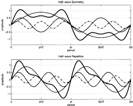
fort. The situation is reversed for even harmonics-the line demands large currents, nulling the source voltage. Under these conditions the periodic steady state voltage at the driven port of the line will consist exclusively of odd harmonic components and the current even harmonic components. The signals will then be half-wave sym-metric and half-wave repeating respectively, a fundamental result of Fourier analysis. By way of illustration, two signals are constructed with arbitrary combinations of even and odd components in fig. 2.2. In each plot the sum is depicted by the heavy line. The sum in the top plot, composed exclusively of odd components is half-wave symmetric. In the bottom plot, the even components result in a half-wave repeating sum.
The 4D inverter, fig. 2.3(a), consists of a shorted quarwave transmission line ter-minating at the drain-source port of its switch and a resonant output tank. While the quarter-wave line enforces drain voltage symmetry in periodic steady state, it is the interaction of the tank with the shunt capacitance, Cp (usually device parasitic capacitance, although external shunt capacitance may be added), that ultimately
2.1 The class 4) Inverter
Half-wave Symmetry
0 o5 pi/2 ... .. . . .p.. . . . .p.. . . . . .. . . . . -0 .5 - -. --. -.- .. . - - -
-o pi/2 pi 3pi/2 2pi
period
Half -wave Repetition
0 .5 - - - - -- - - -- - - --
--o a c v- -- of ac hievin - -e--o-- ---- --- ---
e-C11
0 pi/2 pi 3pi/2 2pi
period
Figure 2.2: Half-wave symmetric and half-wave repeating waveforms.
creates ZVS and high efficiency. Considering the waveforms in fig. 2.3(b) the drain voltage is clearly half-wave symmetric. It has a dc average component equal to the source voltage, a condition of achieving periodic steady state, which also serves as the axis of symmetry. The switch holds the drain node at ground for a portion of the cycle defined by q(t). When the switch turns off, the line current falls abruptly to zero and the load current charges Cp to the peak drain voltage, 2VIN, a value that results from reflection about the DC average'. Once Cp has charged to 2VIN, the line current again equals the load current, and the drain voltage remains constant. After a period equal to the switch on-time, the line current falls to zero and the load current discharges Cp, ringing the drain to zero and creating an opportunity for the switch to turn on without loss.
It is important to note that the symmetry in drain voltage does not guarantee ZVS. For instance the waveforms in fig. 2.4 show what would happen if the value of Cp is halved. The load network draws too much charge out of the capacitor and the
'One can also consider that the switch effectively launches a voltage wave of -VIN down the line which must return a half cycle later inverted to satisfy the boundary conditions established by the short. With a dc average of VIN the additional VIN from the returning wave adds to the peak voltage, 2VIjp,.
-ULN4 LRES
R ES jL
VIN q SW Cp
+ quarter-wave qt RL
(a) Class <D Inverter
<D Converter Waveforms - -I - - - -I -.- -.- -. -V drain ... .... -- - -- - - --.-- - -- q (t) ) 5 10 15 20 25 30 35 40 45 5 Time [ns] ) 5 10 15 20 25 30 35 40 45 5 Time [ns] 0 0 0 5 10 15 20 25 Time [ns] 30 35 40 45 50
(b) 50 MHz Class <P Inverter Waveforms
Figure 2.3: The class 4D inverter tuned for soft switching at 50 MHz. The shorted quarter-wave line ensures the drain voltage is half-wave symmetric. The rising and falling edges of the drain voltage are due to the charging and discharging of C, each cycle by the difference between iulne and iobad Important to note is that the ZVS condition is not guaranteed by half-wave symmetric voltage alone. The load network and switch capacitance must interact so that the drain voltage reaches zero at the appropriate moment. See appendix A for component values and simulation files.
30 20 -a 10 E 0 1 0 E -1 . . . .. .. . . .. . .. .. o a " I I .. I . . . E 3 2 0 ' .... ... . . . ... . ... .. . .. ..... .... .. .... ... .. .... S W - ~ ~ ~ ~~~ - - --. - - - -- - - -.. -- - C P
2.2 The class (D2 Inverter
Detuned (D Inverter Drain Wavform for CP =CP/2
50 40 -- - - ->. 30 20 -10 - - - - -E 0- --10 - - - -0 10 20 30 40 50 Time [ns]
Figure 2.4: In the I) inverter, the transmission line enforces half-wave symmetry. When the load network and shunt capacitance Cp are unmatched, loss results at both transitions. Component values and simulation files can be found in appendix A
drain voltage undershoots zero. The symmetry enforced by the line then causes a corresponding overshoot one half-cycle later. This operating condition forces the switch to dissipate energy from the capacitor each half-cycle, a lossy proposition. Limits on power delivered to the load at a given Cp, frequency, and input voltage naturally arise where all the energy stored on Cp must come from the load side. In steady state, the load current must be exactly the right value to ring the drain to zero. Once the duty ratio has been constrained, the tank current is fixed, and so is the output power because the load resistance necessarily plays a role in determining
the tank current. Since Cp is smallest when composed exclusively of device parasitic capacitance, there is a minimum power delivered to the load for a given switch, switching frequency, and input voltage. The (2 inverter, having the ability to absorb
device capacitance into either the load network or its source network has greater freedom in this regard.
2.2
The class
(D2Inverter
The class j2 inverter, like the 4 inverter, exploits waveshaping techniques to realize approximate half-wave symmetry and the related benefits. It diverges on the point of how many harmonic-coincident resonances are employed to achieve the effect. Where the ideal D inverter relies on an infinite number of harmonics, the 4)2 network seeks to control only the first three. The resulting approximate half-wave symmetry reaps
-Input Network Impedance so 60. L2F LF Cp ~ 20 . .... C2F * --2 0 --...-- - ...-- -. - - - - --ZIN 540 ' O ' 1oFrequency [Moz]0
(a) 1)2 Input network (b) Bode Plot of ZIN
Figure 2.5: The impedance of the (D2 input network can approximate a shorted quarter-wave transmission line.
the rewards of ZVS yet allows greater flexibility in establishing the details of the waveform shape while avoiding need for many resonant elements. Key to meeting the requirements of integration, this flexibility also comes with reduced design com-plexity. Practical implementations of the class 4 inverter control perhaps a dozen harmonics [2, 24]. The associated multi-resonant structures require significant design effort, are sensitive to process variation, and difficult to change. In contrast, the
2 inverter's low-order lumped network can be readily tuned to establish a desired
impedance, reducing the design effort.
For instance, the lumped network depicted in fig. 2.5 has an impedance characteristic that is identical to that of the shorted quarter-wave transmission line for the first three harmonics. When the component values are selected according to eqns. 2.1 the poles occur at the fundamental and third harmonic with a second harmonic zero.
1 1 15
LF = L2F = 2F = -CF (2.1)
91r2fgWCF 157r2f~wCF 16
This network can viewed as a parallel combination of series- and parallel-resonant tanks. The series tank, L2F and C2F, is tuned to the second harmonic, creating the zero. The inductor LF in the parallel tank provides the low-frequency asymptote
and resonates with the other elements to create the peak at the fundamental, and the capacitor CF provides the high-frequency asymptote resonating with the other
elements to created the peak at the third harmonic.
The addition of a parallel switch and an output tank comprised of RL, CRES, and
2.2 The class 12 Inverter
L L RES
-VIN L2F q M RL
C2F C
Figure 2.6: The 4D2 Inverter.
the J inverter is replaced by the lumped network of fig. 2.5(a). CF becomes the switch capacitance plus any shunt capacitance added at design time. The output "tank" can be dealt with in several ways. Used as a resonant tank, it may be tuned to look resistive at the fundamental or slightly inductive to aid switching (it could be tuned to look capacitive, but greater circulating currents exacerbate loss). As an alternative, the capacitor CRES can act as a dc block while LRES and RL function as an impedance divider to control load power.
2.2.1
Basic Operating Principles
In the 12 inverter we have a network with a second harmonic short, and high
impedance at the fundamental and third harmonic. Ignoring, for the moment, higher frequency content, the network will support predominantly odd harmonic voltages (fundamental and third) thus sharing the same half-wave symmetric properties as the (J) inverter. Each cycle the switch forces the drain voltage to zero for a period
DT, where D is the duty ratio. At turn off the network rings to roughly twice the dc
average voltage at the drain, 2. VIN, before heading towards zero and the beginning of the next cycle. Under these conditions, zero voltage switching permits efficient operation.
The simulated waveforms in figure 2.7 indicate the true operation is more complicated. The drain voltage peak is not the mirror-image plateau of the 4b inverter. Instead, telltale humps arise as they must where the harmonic content is limited. Half-wave symmetry is exposed as approximate by the same, indicating that some even order
-<2 Inverter Wavforms - Vd drain I- .. . .. . - t 5 10 15 20 25 Time [ns] 30 35 40 45 50 5 10 15 20 25 30 35 40 45 5( Time [ns] ) 2 0 -21 5 10 15 20 25 Time [ns] 30 35 40 45 50
Figure 2.7: The 4D2 inverter tuned for operation at 50MHz. The drain voltage displays only approximate half-wave symmetry because the network only con-trols the first few harmonics. Notice that the switch current is substantially similar to that of the 4I inverter (fig. 2.3(b)), but the other currents depart creating the telltale (I2 humps. Component values and simulation files are in
appendix A E 30 20 10 0-0 A. 5) E 2 0 -2 E ... load % ... ... .... . . ... ... . MR *% ... ... ... ... .. ... ... ... ... .. ...
-2.2 The class (2 Inverter
First Three Harmonics
VV
1. .- -.- ... -. -. -. -...--.-..
0-0 10 20 30 40 50 First Six Harmonics
4 - --- lump
2 -- -. . . .. . -. --.
-fline
0 10 20 30 40 50 Time [ns]
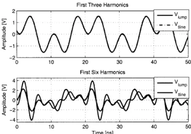
Figure 2.8: In the top plot both an ideal quarter-wave transmission line and the lumped network process the first three harmonics identically. When higher frequency content is added at equal power, the behaviors diverge. The trans-mission line still enforces half-wave symmetry, but the lumped circuit does not.
harmonics play a role in determining the drain waveform. Nevertheless, the system's
behavior is within a stone's throw of what might be expected: there is approximate half-wave symmetry.
Figure 2.8 shows how the 42 input network and a shorted quarter-wave transmission line compare in handling signals of differing harmonic content. When the drive current is composed solely of the first three harmonics, all equal in amplitude, the resulting voltage is exactly half-wave symmetric just as the shorted quarter-wave transmission
line case. When equal amplitude components of the first six harmonics are applied, the response differs substantially from the ideal line. If the assumption of approximate
half-wave symmetry is to be valid, most of the energy in the drive signal must be in
the first few harmonics.
A useful way to define a drive signal in the 42 inverter is found in methods com-monly associated with the harmonic balance technique [29]. The harmonic balance technique, used as a computationally-lightweight means of solving the for the steady state response, relies on separating a circuit into a minimum set of linear and non-linear subcircuits. By then splitting the subcircuits at their common terminals and augmenting them with independent sources, each source can made to produce a drive signal where all the terminal variables are consistent (by means of an optimization
12 0
+ V
2(t)
S1 V,(t) f S2
. -1(t)
Figure 2.9: Splitting a circuit into two subcircuits.
--- ---I LFA A'i1) (t) L I - ~(~V(t) c RL CF RV(t) V F V I2N ~ C2F V) 0 C2F L :Vt) L CR CR - I - B B'
(a) 4P2 inverter (b) 4)2 inverter split into subcircuits
Figure 2.10: <P2 inverter broken down into subnetworks. The network on the left hand side of figure (b) is the complete drain-source network with drain-source
impedance ZAB. The MOSFET is replaced by a linear independent current
source, I(t).
algorithm, for instance), at which point the solution is known. For example, figure 2.9 depicts a circuit consisting of two sub-circuits, Si and S2 that share the variables
V(t) and I(t) at their terminals. The network is split as illustrated, where Si now has a drive current 11(t) and S2 a drive voltage V2(t). If a unique solution exists among the branch variables of the sub-circuits, when Ii(t) = 1(t) and 2(t) = V(t), then I(t) = I2(t) = I(t) and V1(t) = 2(t) = V(t). This amounts to the substitution of sources for subcircuits. In the case where a complete circuit is nonlinear, that portion
can be replaced with a linear source and the resulting subcircuit is linear.
When this technique is applied to the (D2 inverter in fig. 2.10, the obvious choice for the nonlinear sub-circuit is the only non-linear element, the MOSFET, outlined in fig 2.10(a). The balance of the circuit forms a completely linear sub-network shown as