Design and Manufacture of the Next
Generation of Ion Electrospray
Thrusters
by
Dakota S. Freeman
S.B., Physics and Mechanical Engineering,
Massachusetts Institute of Technology
(2016)
Submitted to the Department of Aeronautics and Astronautics
in partial fulfillment of the requirements for the degree of
Master of Science in Aeronautics and Astronautics
at the
MASSACHUSETTS INSTITUTE OF TECHNOLOGY
June 2019
@Massachusetts
Institute of Technology 2019. All rights reserved.
Signature redacted
A uthor ...
...
Department of Aeronautics and Astronautics
Signature redacted-
May
23, 2019
C ertified by ...
...
Paulo C. Lozano
M. Alemin-Velasco Professor of Aeronautics and Astronautics
Thesis Supervisor
Accepted by
...
Signature redacted...
Sertac Karaman
MASSACHUSWTSINSTITTE
Associate Professor of Aeronautics and Astronautics
Chair, Graduate Program Committee
JUL,
01 1
2019
Abstract
In this thesis, a full re-design of the iEPS 2.3 system developed by the Space Propulsion Lab has been undertaken, producing its 3.0 incarnation. Each sub-component and as-sembly has been investigated and improvements to them explored, recommended and implemented. The supporting frames and extractor electrodes have undergone modifi-cations and a full process re-design, respectively, in order to improve the reliability and performance thereof. Much of the work described in the following pages has focused around solving a core problem of emitter flooding - that is, excessive wetting of the emitter substrate before it can be fired, leading to a short-circuit and a failed engine.
To this end, a solid-state valve which employs the electro-wetting phenomenon, and the supporting architecture for the same has been developed and integrated into a full thruster package. This has been tested in flight-like conditions and shown to reliably prevent the described failure mode without interfering in the overall performance, even rendering it more resilient to intermittent spikes in emission.
In addition, two new materials to replace the current borosilicate glass emitter chips have been investigated, one made in-house and the other purchased off-the-shelf. Both were tested in overall current vs. voltage performance, time-of-flight spectroscopy and retarding potential analysis. The former material, while not fully developed, has nonetheless displayed remarkably promising results, outputting very high current in the pure ionic regime.
Thesis supervisor: Paulo C. Lozano
Acknowledgements
I would first like to take the opportunity to thank Professor Paulo Lozano, who has been an incredible adviser, both as a graduate student and as an undergraduate, almost five years ago now. His positivity and enthusiasm for the projects have made it a pleasure to learn and work in the Space Propulsion Lab.
While all of the members of the SPL have been wonderful and many of you have helped, I'd in particular like to thank my lab- and office-mate Bjarni Kristinsson, with whom I have worked closely for much of the past two years, and without whose help it would not have been possible to cover nearly as much ground, and Elaine Petro, who donated far more time than she really had to in helping with trouble-shooting
and developing particular aspects of this project which otherwise seemed endless. To my wife, Roksi Freeman, thank you, for your endless support, for patiently listening
as I ranted about processes not working, or to my excitement when they did, and for always being there for me.
Contents
1 Introduction 13
1.1 The Tyranny of the Rocket Equation and a Need for Small Satellite
Propulsion . . . . 13
1.2 Electrospray Propulsion . . . . 14
2 Current Design 16 2.1 Overview of the components . . . . 16
2.1.1 The frame . . . . 16
2.1.2 The extractor . . . . 18
2.1.3 The emitter . . . . 19
2.1.4 The cap . . . . 21
2.1.5 The tank and subtank . . . 22
2.1.6 Distal electrode . . . 23
2.2 Fabrication order of operations . . . 24
3 iEPS Frame Redesign 26 3.1 Issues with current design . . . 26
3.1.1 Flow rate limiting . . . 26
3.1.2 Consistency of bond line . . . 27
3.1.3 Low yield and structural integrity . . . 28
3.2 Design Changes . . . 28
3.3 Revised Process Flow . . . 31
4 Extractor redesign 33 4.1 Challenges with current design . . . 33
4.1.1 Interception current . . . 33 4.1.2 Difficulty of manufacture . . . 34 4.2 Design changes . . . 36 5 Valve Designs 39 5.1 Motivation . . . .. . . . 39 5.2 Design Requirements . . . 39
5.2.1 Simplicity of actuation . . . 39
5.2.2 Simplicity of integration . . . 40
5.2.3 Passive robustness . . . 40
5.2.4 Active robustness . . . 40
5.3 Electro-wetting valve . . . 40
5.3.1 Preliminary Functionality Testing . . . 42
5.3.2 Robustness . . . 44
5.3.3 Revised design . . . 44
5.4 Valve development . . . . 45
5.5 Metal diaphragm valve . . . . 46
5.5.1 Testing . . . . 47
6 Valve development 49 6.1 Motivation . . . . 49
6.2 Valve-test assembly design . . . . 49
6.2.1 Initial assembly procedure . . . . 49
6.3 Environmental testing . . . . 52
6.4 Caveats and issues . . . . 53
6.5 Revision of valve design . . . . 55
6.6 Results from testing . . . . 56
6.7 Final design and integration onto tank . . . . 57
7 Photolithographic Fabrication 62 7.1 Techniques in MEMS . . . 62
7.1.1 Standard processing flow . . . . 62
7.1.2 Oxidation techniques . . . . 62
7.1.3 Contact and contactless photolithography . . . 65
7.1.4 Wet processing . . . . 67
7.1.5 DRIE . . . 69
7.1.6 W afer bonding . . . 70
7.1.7 Deposition techniques . . . . 71
8 Componenent Manufacturing 8.1 Frame manufacture ...
8.1.1 Base layer ... 8.1.2 Insulating layer ... 8.1.3 Alignment layer . . . 8.1.4 Anodic bonding and c 8.2 Extractor manufacture . . .
8.2.1 Structural layer . . . 8.2.2 Grid layer . . . . 8.2.3 Si bonding and gold c 8.3 Valve manufacture . . . . . 8.3.1 Preliminary design . 8.3.2 Final process . . . . 9 Material research 9.1 Goals . . . . 9.2 "Mystery glass" . . . .. 9.2.1 Laser-induced fusing 9.2.2 Test firing . . . . 9.3 Silica production . . . . 9.3.1 Binder materials . . 9.3.2 9.3.3 9.3.4 9.3.5 9.3.6 dicing oating Forming methods . . . . Initial results -hydraulic press Casting . . . . Process flow . . . . Laser ablation . . . .
10 Thruster Firing Results
10.1 Firing data . . . . 10.1.1 RPA . . . .
10.1.2 Time of flight spectroscopy . . . . 10.2 DG Silica . . . . 75 75 75 79 81 84 85 87 88 89 90 90 91 95 95 96 97 99 100 100 100 102 102 104 106 107 107 109 111 113
10.2.1 DG IV Curve ... 114
10.2.2 DG RPA Results . . . 115
10.2.3 DG Time-of-Flight Results ... 116
10.3 "M ystery Glass" . . . 116
10.3.1 Mystery Glass IV Curve . . . 116
10.3.2 Mystery Glass RPA Results . . . 118
10.3.3 Mystery Glass Time-of-Flight Results . . . 118
10.4 Full thruster testing . . . 119
List of Figures
1 A fully assembled and mounted thruster board assembly 2
iEPS
3.0 fram es. . . . .Side view of a frame . . . . A n extractor . . . . Extractor damage caused by interception . . . . Comparison of good and bad emitters . . . . CAD for the tank components. . . . . Thruster electrode pieces . . . . The components that make up a thruster. . . . . A fully populated thruster board . . . . Inhomogeneous thrust from an emitter . . . . Spot welding damage on frames. . . . . A revised LI wafer . . . . A redesigned frame
1
. . . . Bonding overspill on the inner edge of the frame . . . . Masks for new pedestals for frames . . . . Origninal and revised frame layer one processes . . . . A taped-up extractor . . . . Current extractor design process flow . . . . Sample pressure and vibration curves . . . . Diagram of valve integration into thruster . . . . Comparison of contact angles . . . . Setup for preliminary valve tests . . . . Duration test setup . . . . V alve lip . . . . Valves in the sputtering jig . . . . The parts of the diaphragm valve . . . . An actuated diaphragm valve. . . . . The layout of the valve development testing components . . . . . 30 Testing the hydrophobiity of a developmental valve . . . .14
. .
. . 50 . . . . 16 . . . . 18 . . . . 19 . . . . 19 . . . . 20 . . . . 21 . . . . 23 . . . . 24 . . . . 26 . . . . 27 . . . . 29 . . . . 29 . . . . 30 . . . . 31 . . . . 32 . . . . 32 . . . . 35 . . . . 36 . . . . 41 . . . . 42 . . . . 43 . . . . 43 . . . . 44 . . . . 45 . . . . 46 . . . . 47 . . . . 48 . . . . 50A developmental valve setup . . . . A developmental valve beaker assembly . .
The vibration and pumpdown setup . . . .
Fluoropolymer lift-off with acetone . . . . . A actuated valve . . . . Finalized tank design with PTFE collar . . The two different PTFE collars that were tes 38 A boat of oxidized wafers
51 52 53 . . . . 54 . . . 56 . . . 59 ted . . . 59 . . . . 64
DRIE silicon etching via the Bosch process . . . . Basic sputter coating schematic. . . . . Dicing an extractor wafer . . . . Masks for the base layer . . . . A finished Li wafer . . . . An L2 wafer . . . .
Insulating layer process flow . . . .
A partially completed HNA etch . . . .
Alignment layer process flow . . . .
Alignment layer masks . . . .
L1-L2 bond . . . .
Two-part extractor process flow. . . . .
Schematic valve fabrication process . . . . Valve apertures undercut via isotropic etch . . . .
A tip etched in borosilicate glass . . . .
An array etched into a "mystery glass" chip . . . . Fused crust . . . . The MG glass pre- and post- BOE . . . .
MG crust delamination . . . .
Hydraulic press and die. . . . . An aluminum mold for casting silica . . . . Samples of the new DG silica material . . . .
A patterned DG emitter . . . . 31 32 33 34 35 36 37 69 73 74 76 79 79 80 81 82 83 86 87 91 93 95 96 97 98 99 101 103 105 106
. . . .
. . . .
The tip of a DG emitter . . . 107
Schematic of the IV curve apparatus . . . 108
Schematic diagram of the RPA setup . . . 110
A schematic view of the time-of-flight system . . . 112
An example of time-of-flight data as measured by oscilloscope . . . 113
The IV curve for a DG silica thruster . . . 114
An RPA curve for a DG thruster . . . 115
DG silica time-of-flight results . . . 116
Mystery glass IV curve . . . 117
RPA curve for an MG thruster fired at 2.3 kV . . . 118
Time-of-flight results for a "mystery glass" thruster . . . 119
Full thruster current emission profile . . . 120 62 63 64 65 66 67 68 69 70 71 72 73
List of Tables
1 Simplified
iEPS
2.3 extractor process flow . . . 372 Step-by-step vibration and depressurization procedure. . . . 53
3 Results from valve development . . . 57
4 Summary of valve integration approached and results . . . 58
5 Process flow for revised LI wafers. . . . 76
6 Preliminary process flow for electrowetting valves . . . 90
12
1
Introduction
1.1
The Tyranny of the Rocket Equation and a Need for Small
Satellite Propulsion
A basic truism in rocketry is that to get where you want to go, you can either expel a great amount of mass "slowly" -a word which here means only just north of supersonic
- or expel a small amount of mass extremely quickly. This is well summarized in Tsiolkovsky's rocket equation.
-f=
exp
-(1)tmj
This states that the ratio of the final mass to the initial mass after a maneuver or set of maneuvers requiring some given Av has an exponential dependence on the ex-haust velocity c. Therefore, it is efficient from a design perspective to have as high an exhaust velocity as possible to maximize the allowed payload, which in turn requires minimizing the ratio of initial to final mass, with the caveat that this trade-off presents being that if you choose to optimize on the high-velocity side of things, typically your punishment will be that your maneuvers will take much longer - a course that might have taken several days could now be several months.
However, if the payload is a satellite and not several live humans, the trade-off in time for efficiency may well be worth it. Currently, there is a major hole in the panoply of propulsion systems - there is no small, high-efficiency option for groups that lack the capital to install a large, telecom-sized satellite in orbit for their research projects. Typically, these groups opt for small, off the shelf systems such as CubeSats, which, with their 10x1Ox1O cm size and sub 1.5 kg mass, are easy to piggyback on launches of those larger satellites at a much more affordable rate. However, the drawback here is the relative lack of attitude control, since reaction wheels are bulky and massive by necessity and that allowance could be better used by the actual experiments and instrumentation, and the complete lack of orbital control. While this might be
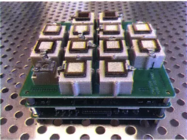
accept-Figure 1: A fully assembled and mounted thruster board assembly. On the bottom left is a sensor designed to determine when the thrusters are ready to fire.
able for some lines of research, it closes down many others such as coordination of multi-satellite "constellations" for networking. It is this paradigm in which the Ionic liquid Electrospray Propulsion System (iEPS) operates.
1.2
Electrospray Propulsion
The principals behind electrospray propulsion are similar to those in other electric propulsion schemes; a high bias voltage is applied between an electrode and some kind of propellant, which is thereby accelerated to high velocities (from several thousand to several tens of thousands of meters per second), producing thrust. Electrospray thrusters are purely electrostatic and do not require magnetic confinement; rather, the bias voltage is applied between an extractor grid and propellant directly, which causes ions to evaporate from the liquid and produce current. This thesis is focused specifically on ionic liquids, which are salts that are molten at room temperature.
In the iEPS configuration explored here, the system employs a passively-fed approach to allow liquid to be transported through an array of tips etched into a porous medium. The tips have the geometric effect of drastically enhancing the local electric field, in a mechanism similar to coronal discharge. This allows a lower potential, in the
1
kVrange, to be used. When the voltage is applied, the liquid is pulled up into Taylor cones, which are the results of the balance between the electrostatic forces and the surface tension of the liquid; as the Taylor cones have an extremely small radius of curvature at the apex, the electric field is further enhanced to the point where ions begin to evaporate directly from the meniscus. It as at this point that they are accel-erated by the high potential to produce thrust.
Ion electrospray thrusters have moderately high specific impulse, often in the range of 1000-2000 seconds.
The work describe in this thesis seeks to expand upon that done by Louis Perna and Dan Courtney, creating what is effectively the 3.0 version of the iEPS thruster. [1] [2]. Chapter 2 is a brief overview of the current design and the terminology used within this thesis, which has become quite specific to the iEPS project as it has developed. Chapters 3 and 4 focus on the issues with the frame and extractor components, and how those problems might be addressed from a design basis. Chapter 5 considers a new component, a flow-restricting valve that will sit in-line with the rest of the architecture. Chapter 6 delves more into the development of the valves, culminating in chapter 8, which explores the actual fabrication procedures for each of these components, for which chapter 7 serves as an introduction to the required techniques and their use in the scope of the project. Chapter 9 moves on to look at alternate materials for emitters, while chapter 10 looks at the results all of these changes have produced.
2
Current Design
2.1
Overview of the components
Following is a high-level overview of the thruster manufacture process; it does not go into specifics of the micro electromechanical systems (MEMS) fabrication techniques used in the frame, extractor and valves, which will be explored in greater detail in their relevant sections, and full process flows for each may be found in the appendices. At each stage, please note the terminology used, as it will frequently be used throughout this thesis.
2.1.1 The frame
The frame is the base of the emitter. It is fabricated via MEMS processing techniques and consists of three layers: a base layer, called L1, a glass insulating layer, L2, and a third alignment layer, L3. While Li and L3 are both silicon, the insulating layer, as its name indicates, serves to electrically isolate the base from the alignment layer, which is crucial to the operation of the thruster as it allows a high potential to be applied between the chip and extractor without it immediately shorting.
Figure 2:
iEPS
3.0 frames.There are several features of the frame that have been named:
The outer frame is the main structure, on which the posts sit. Its thickness adds
some structural strength to the frame,since although silicon is reasonably hard, it is also quite brittle. In testing the strength of the bond, it was found that the frame typically would shatter before the bond would fail after loading more than a kilogram
of mass directly atop the frame.
The inner frame is the part of the frame on which the emitter chip sits; adding the gap between the inner and outer frame means that any liquid that leaks from the chip would have a much longer path to make it to the posts where they could potentially short the thruster.
The port is the open area of the inner frame that would connect the emitter chip to the tank and propellant reservoir. Typically, it is not referred to as such until after the emitter chip is actually bonded to the frame.
The bridge connects the inner and outer frame. Keeping this clear of debris helps to prevent liquid creeping across it; the primary source of which is from excessive adhe-sive being forced out of the bond line and subsequently partially ablated during laser patterning.
The posts are the mounting and aligning points for the extractor, as well as hold-ing the alignment marks, the features for the ablation pattern. These features are etched no more than three hundred nanometers deep, meaning that they are quite delicate and care must be taken not to damage them. While it is possible to align the laser pattern to the frame with only two markers intact, best practices dictate that they should ideally all remain pristine.
In addition to the path-length precautions introduced by the inner frame/outer frame construction, note also the shape of the insulating layer. The sharply concave geometry, an artifact of the isotropic etch that is used to form it, serves to further inhibit liquid impingement on the extractor due to the fact that liquids typically do not easily navigate sharp corners but rather are pinned by them.
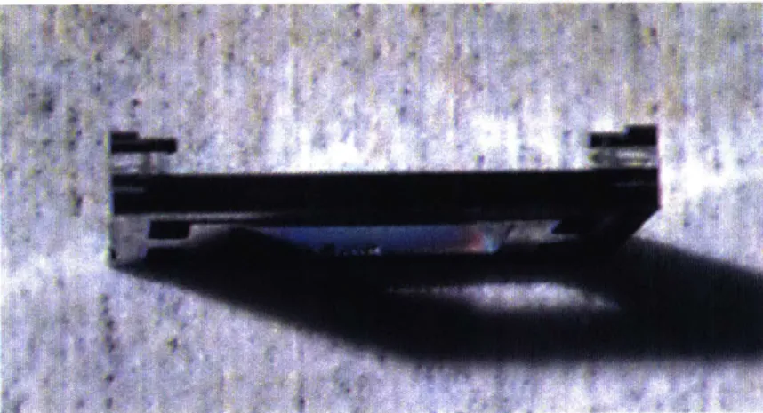
Figure 3: The side of a frame. Note the multiple different layers and the edge geometry of the middle glass layer.
2.1.2 The extractor
In order to produce a current and hence thrust, it is necessary to apply a voltage to the substrate. The extractor electrode forms the other part of the anode/cathode pair (which one depends on the mode of operation). It is made from silicon using a similar set of MEMS techniques as the frame, which allows for the small apertures (less than 350 microns) spaced closely and evenly together penetrating a thin membrane, match-ing the pattern of tips ablatively etched into the emitter substrate. The apertures are designed to be as large as possible and the membrane as thin as possible so as to present as little material in the way of the beam as possible. Below a certain thick-ness clear flexure of the membrane could be observed, suggesting that the durability of the membrane may not be overlooked, despite the solid-state nature of the operation.
It can clearly be seen that the extractor has been coated with gold. In fact, for ma-terial compatibility reasons, it is gold over a thin layer of titanium, the interim layer promoting adhesion between the gold and silicon. This is not just to make the extrac-tors look good, although it achieves that admirably; it has the dual functionality of preventing the native oxide layer that forms on silicon in atmosphere (during storage, since this is obviously a non-issue in space) from growing thick enough to interfere with the electrical connection and to ensure that the fully conductive surface is capable of easily dispersing any current that is intercepted by the extractor. Doing this helps to
Figure 4: An extractor.
Figure 5: Extractor damage caused by interception
prevent or at least reduce any damage that could be caused by the excess current, by Joule heating or physical sputtering.
2.1.3 The emitter
What is referred to as the emitter is comprised of two parts: the emitter chip and the frame. The emitter chip is simply a piece of porous borosilicate glass, originally de-signed for use in filtration systems. The chip must be filed and polished to the correct dimensions, such that it sits neatly in the bonding jig and the top surface is flush with the alignment marks. Doing so ensures that the patterned tips are as level as possible and ideally flush with the alignment marks, though of course some removal is all but inevitable to be required. It is bonded to the silicon frame with a low-temperature melting point leaded glass sealing paste, which provides a high-strength bond with no
4
Figure 6: Comparison of good and bad emitters. The left-hand emitter shows consid-erable variability and some debris that must be removed, while the right-hand emitter has been reworked.
risk of contaminating chemicals. Alternatively, a low-outgassing epoxy may be used, but there is a degree of uncertainty to this as in the past, some epoxied emitters ex-hibited excessive ablation in the region above the bond itself, as may be seen much later in figure 54. Changes to the laser patterning method seem to have mitigated this failure mode, but more work is likely necessary to understand the mechanism behind either the excessive ablation or the mitigation thereof.
The patterning itself is carried out using a solid-state picosecond laser, emitting co-herent light at 248 nm. The energy in each pulse is sufficient to directly ablate the glass, which is efficient at absorbing ultraviolet light. Fortuitously, a change made to the pattern itself, shifting from the natural hexagonal pattern to a square pattern decreased the complexity of pattern generation, the number of lines required (and thus time and cost per emitter) while actually improving the quality of the results.
After the ablation process, there are frequently debris and imperfections left on the surface of the emitter that must be cleaned up by hand, under a microscope. This is, of course, difficult from the perspective of manual dexterity as the pitch between emitter tips is 450 pm and they are extremely delicate, so there is very little room for error. In order to mitigate the risk of flooding, the emitter is coated on all sides except the port a with a hydrophobic layer, for which multiple materials may be used.
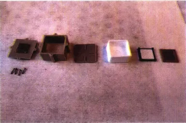
Figure 7: CAD for the tank components.
2.1.4 The cap
The cap serves multiple purposes. It is the interface for both the emitter and the subtank, as well as the mounting point for the tank shell. It has several structural
features to facilitate each of these.
As may be seen in figure 7, the sub-tank mounting point features two raised semi-sharp ridges. These have the function of providing a good seal in conjunction with the outer shell. Even without the additional support from the shell, the seal is resilient to ionic liquid intrusion, likely thanks in part to the hydrophobic nature of the teflon. Through this attachment point, a hole has been drilled to fit the electrode, providing a path by which the ionic liquid may reach the emitter.
The emitter itself is mounted to the stepped feature atop the cap. The first step serves as an offset between the cap and the bottom of the frame, providing an additional line of defense against any propellant leakage. While unlikely, it could represent an absolute failure mode if ionic liquid breached the emitter and flowed to the PPU, where it could play havoc with the circuitry. As such, it is important to prevent. The second step
serves to center the emitter on the tank cap, as it matches to the inside of the frame. It is on this corner between the first and second steps to which the epoxy is applied. Finally, the small third step -little more than a notch in the top pedestal -is intended to allow space for any excess adhesive that may have been applied around the inside edge of the emitter chip/frame bond line, while ensuring that the wick is still in good contact with the chip.
2.1.5 The tank and subtank
The tank consists of two parts: the shell and the sub-tank. The sub-tank is machined from teflon. This is a useful material for a variety of reasons. Teflon has good physical properties; its chemical compatibility means it will not react with the ionic liquids, while its relatively high degradation temperature (approximately 250'C) gives a wide range of operational latitude.
While the sub-tank is vital for the containment of the ionic liquid, it is not in itself structurally sound enough without additional support. Therefore, an enveloping shell made of PEEK (polyetheretherketone) was added. PEEK was used rather than the more common teflon due to its higher rigidity - very important considering how thin some of the features can be - and the fact that, unlike teflon, it does not degrade when subjected to UV light or oxygen plasma. The shell supports the sub-tank.but only contacts with a few small ribs, to ensure as much surface area of the sub-tank as possible is unobstructed and can easily vent to the ambient, through the set of holes that have been drilled into the side of the tank. The holes are smaller than the Debye length of the atmospheric plasma to which the thruster may be exposed, which is roughly 1 mm in LEO, so it does not present an undue risk to the underlying material.
On the top and bottom of the shell are a set of 000-120 tapped screw holes, for securing the cap with its bonded emitter and valve, and for mounting it to the electronics board. Of course, size 000 screws are quite delicate so great care must be taken when turning them.
Figure 8: The two stages of the electrode assembly. The left-hand electrode has not yet been pyrolyzed, which causes the electrode to shrink and carbonize.
2.1.6 Distal electrode
In order to extract current, it is necessary to have both an anode and a cathode. It would be a natural assumption to make the emitter substrate one of the electrodes, opposite the extractor, but this turns out to be a sub-optimal choice. The central reason for this is the potential for electrochemistry. Ionic liquids are potentially pow-erful electrolytic etchants on a variety of surfaces, so if electrochemistry occurred on the surface of the emitter substrate, it is highly likely to cause a degradation in per-formance over time as the tips erode and become damaged. To avoid this, a distal electrode was added, formed from porous carbon xerogel, removed from the emitter itself. Thus, any electrochemical damage caused during operation will not affect the emitter itself. [3]
Figure 9: The components that make up a thruster.
wick and transport fluid to the emitter substrate. The wire connection to the electrode is made of platinum, which has excellent resistance to electrochemical processes, due to its low reactivity. Moreover, its high melting point and resilience to oxidation means that it is well suited to the high-temperatures involved in pyrolyzing the electrode.
2.2
Fabrication order of operations
Following is the order of operations for the manufacture of an ion electrospray thruster, from start to finish. Several of these steps naturally encompass a fairly intricate set of sub-steps, the cleanroom fabrication in particular.
1. In the clean room, fabricate the L1, L2 and L3 wafers and bond them together.
2. Also in the clean room, fabricate the extractor wafer. 3. Dice apart both wafers into the frame and extractor dies.
4. Grind the substrate to the correct size and polish it as smooth and flat as possible. 5. Bond the substrate to the frame, then polish any excess height down such that
the top of the chip is flush with the alignment marks. 6. Pattern the substrate with the tip array via laser ablation.
7. Mix and cast the distal electrodes with integrated wire, then pyrolyze the elec-trodes.
8. Clean and re-work the emitter array, if necessary.
9. Coat the emitters with ceria, allowing the layer to relax in vacuum to become fully hydrophobic.
10. Carefully align and bond the extractor to the emitter, using the alignment fea-tures as a rough guide and the centering of the tips in the aperfea-tures as visual confirmation.
11. Bond the thruster to the tank cap.
12. Thread the sub-tank filling port to accept a 4-40 screw.
13. Pierce the sub-tank at the base and carefully route the distal electrode wire through the hole.
14. Put two pieces of glass filter paper into the hole in the tank cap, then the flow limiter, followed by another two pieces of glass filter paper.
15. Push-fit the sub-tank onto the tank cap, ensuring the distal electrode is correctly fitted.
16. Carefully push the shell onto the sub-tank and cap assembly, being extremely cautious of the thruster.
17. Attach the shell to the tank cap with 000-120 screws.
18. Use a syringe to fill the sub-tank with ionic liquid propellant.
19. Seal the filling port with a teflon 4-40 set screw, ensuring it is flush with the base.
20. Threading the distal electrode wire through the hole, snap the tank base into the shell.
21. Coil the distal electrode wire so it fits neatly into the pocket in the base. 22. Integrate onto PPU.
Figure 10: A fully populated thruster board. The two left-most thrusters feature carbon emitter arrays, hence the darker colors.
3
iEPS Frame Redesign
3.1
Issues with current design
3.1.1 Flow rate limiting
A major issue is that the contemporary incarnation of the frames creates significant spacial variation in the amount of current produced. [13] The issue is likely to be that for propellant to reach the emitter tips on the edges of the chips, it has to travel a greater distance. Given that Darcy's law for flow through a porous medium states
Q A(Pb - Pa) pL
in which the flow rate
Q
is determined by the permeabiltyn
of the medium, the cross-sectional area A, the pressure drop, the viscosity pI and the travel distance L, it can be seen that the flow rate should be inversely proportional to the distance. If the ion current produced is comparable to the maximum flow rates, therefore it will naturally1Z
Figure 11: Inhomogeneous thrust from an emitter, reproduced from Guerra-Garcia et al.
be capped where the hydraulic impedance is greater - at the edges. To resolve this, a new architecture was designed that allows liquid to come in contact with the full reverse side of the patterned area, ensuring that the flow rate will not be the limiting factor. This is achieved by etching a shallow "well" into the inner square of the frame, which enables an even spread of ionic liquid across the back surface.
3.1.2 Consistency of bond line
To ensure high reliability and repeatability, it was decided that it was necessary to develop a method by which a known amount of adhesive (be it epoxy, sealing glass, or some other compound) can be added to the bonding pad in the same spot every time. To do this, two changes were made. Firstly, the previous approach of "painting" the adhesive on was replaced by a pneumatic epoxy pump, capable of dispensing a specified amount of material, based on the pressure and the duration over which it is applied. Secondly, a small channel was added to the bond line. This has two functions; it acts as a convenient guide for the applied epoxy and it also serves to increase the surface area over which the bond acts, thus increasing its durability. This is especially important when bearing in mind the previous change made, in that the size of the bonding area has now been decreased by a significant margin.
3.1.3 Low yield and structural integrity
One persistent and pervasive issue was that the yield of "good" frames possessing all four posts and having no structural defects was lower than desired, on the order of 60 percent. Since the final stage of the frame process entails dicing the wafer apart with a die saw - essentially a slim blade made from resin and industrial abrasive spinning at 30 kRPM - a good deal of stress is applied to the posts. If the bond integrity is not high enough, the posts will break off, ruining the frame from a flight perspective. Therefore, by increasing the area that is bonded, a significantly stronger frame can be produced. This was achieved by extending the quarter-circle plan of the current design into a longer, rounded "L" shape, thereby roughly tripling the area. A major issue is that the bonding method runs counter to the standard mode of anodic bonding, which generally features silicon sandwiched between glass rather than the other way around. [4] This makes the second bond between the alignment and insulating layers much less consistent and indeed this is typically where we see failures, with the alignment layer post de-laminating from the insulating layer beneath.It is likely that in some cases in which rapidly fluctuating current during the bond is observed, much of the area is not well bonded but in fact effectively spot-welded in a small point contact. Therefore, not only would increasing the area increase the strength of a good bond, but it would increase the likelihood that one of these spot-welds intersects with the post and make the frame usable. While one could argue that this might not be durable enough, recall that the extractor, which is epoxied down onto all four posts, provides an additional fixture preventing the failure of more dubious bonds. Regardless, the thrusters will all be subjected to thorough vibration testing and g-force loading before being qualified as flight units.
3.2
Design Changes
A re-designed Layer 1 (LI) die is shown in figure 14. There are several important fea-tures to highlight. Firstly, the inner frame has been widened by 1 min to make room for an etched-in "well" that allows the ionic liquid to flow over the full area of the chip.
Figure 12: Spot welding damage on frames.
Figure 13: A revised Li wafer. The well and moat features are clearly visible; the diffraction pattern at the edges of the wafer is produced by the clamps that hold the wafer to the chuck in the DRIE tool and have no effect on the functionality
Figure 14: A redesigned frame, showing the inserted wick material. Glass fiber is used, as it is able to survive the higher temperatures used in bonding.
To ensure that there is good contact with the ionic liquid, a piece of glass wicking ma-terial is placed in this region before the emitter chip is bonded down, which provides a low-hydraulic-impedance path for the propellant to reach the entire chip.
Widening the inner frame and adding the "well" has two ancillary benefits. Since the inner frame is now as wide as the entire chip, the emitter chip no longer overhangs the frame. While this means slightly more care must be taken when bonding the chip to the frame such that it is aligned well, it also means there is no overhanging material that must be coated with a hydrophobic material, obviating the need for one of the two coating steps that must be done. Additionally, it also means that there is no risk of excess adhesive spilling out on the inside of the chip in a way that will interfere with its bonding to the tank cap.
However, as a result of the widened inner frame, the L-shaped gaps are slightly nar-rower. Therefore, additional care needs to be taken prevent liquid spilling out, crossing the gap and shorting the thruster, which entails very good alignment of the chip to the frame itself, requiring clean bond lines with no overspill and thorough inspection and reworking of the emitter substrate itself. Next, the bond line has been narrowed to 0.5 mm to match exactly the border region of the emitter chip above and accommodate the "well". This ensures that there is a direct straight-line path for the propellant
Figure 15: Bonding overspill on the inner edge of the frame
to the emitter tip and decreases the spatial variation in current emission. Secondly, a "moat" has been etched into the the inner frame to create a convenient place to repeat-ably add the same amount of adhesive, in the same location; since the bonding area has been fairly significantly decreased, it is even more important to ensure consistency.
Unfortunately, due to time constraints, the changes to the post shape were not able to be implemented; they would require four additional masks, two for the L3 and one each for the L2 and L1, and this was deemed a lower priority. Nonetheless, the drawings for the masks that would be used are presented here.
3.3
Revised Process Flow
The revised process is actually not drastically different to the original process; the same steps (with some slight modifications) are followed, but the masks have changed, as can be seen in figure 17. The major modification made is to the backside DRIE of the base layer; in the updated process, a double layer of resist is necessary to protect
Figure 16: Masks for new pedestals for frames. Leftmost: the Li masks; the orange
represents the new pedestals. Middle: the
iEPS
2.0 pedestal mask for L3. Right: iEPS3.0 pedestal mask for L3
the wafer, as the etch is actually several hundred microns deeper.
*~BE
EU
E
E
U
i
no
M
MIN
WE
(a) original Li process (b) updated Li process.
Figure 17: Blue represents silicon, black is oxide and red photoresist.
It is actually unnecessary to modify the processes for the insulating and alignment layers at all; once the new masks are produced, they may be substituted for the equivalent iEPS 2.3 mask with no change to the process flow itself.
4
Extractor redesign
4.1
Challenges with current design
While the current design is overall performing well, there are a few areas that were seen as targets for improvement. The first is the interception current, defined as the current that is "intercepted" by the extractor - that is, the current that impinges on the extractor itself, rather than making it through to produce thrust. While low in the current iteration - generally in the single digits, expressed as a percent of the total emitted current - it can always be improved. Secondly, the current design is quite complex, owing to the the double silicon-on-insulator (SOI) construction and the multiple etching depths that must be obtained.
4.1.1 Interception current
Reducing the interception current is a good idea for multiple reasons. The first is simply a question of efficiency; if, say, the interception current is five percent of the emitted current, that is equally a five percent hit to the power efficiency, since that current cannot produce thrust and the energy used to accelerate those ions is simply wasted. The second is somewhat more subtle; having a high interception current, par-ticularly over a long period of time, can severely damage the operation of the thruster, by either physically damaging the extractor via physical sputtering or, worse, produc-ing a buildup of ionic liquid on the extractor that eventually creates a path to ground for the liquid on the emitter. The former case will cause a slow, slight degradation of performance, but the latter can result in a complete failure of the thruster -once it is shorted, it is no longer possible to produce a bias between the emitter and the extrac-tor, and current/thrust is no longer produced. While it is as of yet unclear whether this happens, it is not difficult to imagine that shorting 1 kV across that small gap could be hugely damaging not just for the now nonfunctional thruster, but also for the PPU or other nearby components. As such, it is desirable to mitigate this current to the greatest extent possible.
divergence is far more difficult to reduce) is simply to reduce the area presented to the diverging beam, such that there is nowhere the current can be intercepted. This may be done by:
" Decreasing the distance between the extractor and the emitter tip. This would effectively move the extractor to a narrower part of the beam. While a simple concept, it has a few associated challenges, primarily due to the fact that it is difficult to precisely control where the tips are relative to the plane of the extractor. This approach has more to do with the emitter and will be further discussed in the relevant sections.
" Making the holes wider. This is a arguably the most straightforward answer, since it does not require any changes to the process, save for changing out the relevant photo-masks. Of course, removing material from the extractor grid will make it commensurately more delicate.
* Making the grid thinner. Since the grid is already extremely thin (45 pm, in the iEPS 2.3 incarnation) it becomes a major challenge to further thin the grid without decreasing the yield significantly.
" Changing the shape of the holes. By giving the extractor holes a diverging profile, a happy medium may be found between structural integrity and reducing the area for interception. It does not remove as much material as would either of the previous two options, but still presents a much greater open area fraction to the beam.
4.1.2 Difficulty of manufacture
Presented in figure 19 is a summary of the iEPS 2.3 extractor manufacturing process flow. As can be seen, the design requires multiple etches at multiple depths, which must be carefully controlled; moreover, due to the inhomogeneous nature of the etching tools, prolonged etching on a single wafer can become an extremely finicky prospect as some parts are thinned significantly more than others. As the process continues, the grid membrane become ever thinner and more delicate, making (potentially catas-trophic) yield losses more of a risk. As such, it is desirable to simplify the process and
Figure 18: A taped-up extractor. This shows how much inhomogeneity there is in the etching process, as dies on the edges are etched considerably more rapidly and must be protected.
make it more robust to minimize the chance of losing dies.
-i-~
N
mob
.0
OXide
J6~
0
SaconGoid
Figure 19: Current extractor design process flow. Image reproduced from Louis Perna's thesis work.
4.2
Design changes
To deal with both of these issues, a new two-wafer process was proposed. One wafer, a single SOI silicon wafer, would become the grid and and alignment layer, while the other would provide structural support and attachment points for the electrical connections. The main benefit of this approach is that it allows for a simple method of producing a diverging profile for the capillaries, while also reducing the number of steps that needs to be done to each wafer and thus the risk of damaging something. However, it does add a bonding step, which itself carries a certain degree of risk, although it is relatively simpler when compared to the bonding step carried out in the frame manufacture. The major change is the revised capillary profile, which now diverges. To achieve this, a brief isotropic plasma etching step is incorporated before the holes are etched through. Due to the highly selective nature of plasma etching, the isotropic etch is able to undercut the oxide layer and produce an overhanging feature. Following this, the wafer is subjected to the standard DRIE process; in the directional and anisotropic regime, the plasma is unable to further etch the area that was undercut and the oxide is now acting as a hard mask. Ideally, this oxide layer should be made thicker than normal (which could be done either by depositing additional oxide, or simply by purchasing suitable SOI wafers) to ensure it has the structural integrity to
iEPS 2.3 simplified extractor process Materials: 150 mm X 750 +
Step Process 0.0 RCA Clean
1.0 Oxidation
2.0 Nested mask patterning .1 Thin resist coating .2 Pattern exposure 3.0 Oxide patterning
.1 Buffered oxide etch .2 Strip resist 4.0 Names etching
5.0 Etch masking .1 Thick resist coating .2 Pattern exposure 6.0 Deep feature etching .1 Device side etching .2 Buffered oxide etch
.3 Device side etching .4 Mount to handle wafer .5 Handle side etching .6 Dismount and strip resist 8.0 Metallization .1 Buffered oxide etch .2 Deposit adhesion layer .3 Deposit conductive layer 9.0 Dicing
40 + 200 Am Double SOI wafer Comments Grow 500 nm oxide Both sides: 1 pm SPR-700 Device side: Grid holes
Handle side: Names and dicing lines Piranha
Handle side: etch two minutes Both side: 10 pm coating AZ-4620, double coat on handle side Handle side: Field square
Device side: Square and alignment holes Over-etch holes into oxide layer Remove oxide in device side square,
handle side field square
Etch to buried oxide layer; holes should punch through to second BOx layer
Device side down
Etch to buried oxide layer, tape as necessary. Remove remaining oxide
10 nm Ti 100 nm Au
Protect dies, two passes per cut.
survive the etch through, as any damage to the oxide layer will quickly be transferred into the grid.
5
Valve Designs
5.1
Motivation
A principal challenge that needed to be overcome in the new version of the iEPS thruster was that of flooding, primarily in the emitter chip.
5.2
Design Requirements
Any valve utilized must be able to achieve the following set of criteria:
1. Be simple to actuate and allow the passage of ionic liquid in a known time in a reliable manner.
2. Be relatively simple to integrate into the existing architecture with a minimum of modification.
3. Resist the intrusion of ionic liquid for an arbitrary amount of time, sitting undis-turbed at room temperature and pressure.
4. Resist the intrusion of ionic liquid under harsh vibrational and pressure loading such that the system would experience at lift-off.
5.2.1 Simplicity of actuation
This requirement states that the valve's usage must be straightforward. Press a button, the valve opens and allows ionic liquid through. This does not necessarily mean that the valve's actuation must be instantaneous; one potential design would take several minutes to hours to open, once the actuation was started. However, it must still be a reliable and quantifiable process, in that either there must be a very uniform set of standards that allow the operator to know the valve is open (for instance, after five minutes at 50 V, when the time-integrated current has reached a certain value or other feed-forward statistics) or have a method of detecting the opening (for instance, one could check continuity between two appropriate points to determine the presence of the conductive ionic liquid).
5.2.2 Simplicity of integration
This requirement holds that the integration into the existing design should be rela-tively simple. Firstly, this means that the physical footprint of the valve, or that of the pieces used to accommodate it, cannot be drastically changed from their origi-nal forms. Secondly, whatever the method of actuating the valve, the changes to the power processing unit (PPU) cannot be major. The reason for both of these is the relative maturity of the requirements and specifications for the PPU and housing for the components, compared to the valve. It would be extremely difficult to make radical changes, qualify them and produce components while staying on schedule.
5.2.3 Passive robustness
Since there is a good chance that the unit will have to remain in less-than-controlled conditions prior to integration into the launch vehicle, it is imperative that the valves be robust to long-term infiltration by ionic liquid. This should entail a static test in ambient condition, for at least several weeks.
5.2.4 Active robustness
On lift-off, the combination of the sudden pressure drop and the vibration is a recipe for inducing leaks. If there is any gas dissolved into the propellant (although care was taken to prevent this) it will come out of solution as the pressure drops, maintaining the raised pressure inside the tank and causing liquid to be forced into any small gaps, in the same way that the increased volume in the passive case could cause failure. Therefore, the valve must be able to withstand this depressurizing/vibration regime in conditions similar to the launch.
5.3
Electro-wetting valve
The concept behind this valve allows for a less destructive and possibly multi-use implementation. It exploits the forced wetting property of liquids - especially ionic liquids -in which a strong electric potential is used to polarize the fluid, which allows it to wet an otherwise hydrophobic surface. [5] The valve itself consists of a matrix of
~12
1 10
Figure 20: Left: an example depressurization profile used for testing; the dotted
line
is nominal pressure and the solid line is measured. Right: An example depressurization profile. Partway through it can be seen that the amplitude was increased to ensure it reached the desired intensity.holes etched through a thin silicon membrane (approximately 200
tim
in thickness). The silicon is then coated with a layer of thermally grownoxide,
sufficiently thick to prevent dielectric breakdown under the applied potential. This is important both for the functioning of the valve insofar as theliquid
becomes polarized relative to the sub-strate, but also that the electronic systems remain isolated and there are no undesired short circuits, since the valve must be grounded relative to the distal electrode. How-ever, it should be noted that, although the extractor electrode is also grounded, the valve cannot simply be attached to the extractor directly - although doing so would simplify the design insofar as it obviates the need for any modifications to the power processing unit (PPU) - since this could cause currentleakage
from any currentinter-cepted
at the extractor. In addition, a relay between the valve and ground could be added as an additional safety factor; once the valve has been wetted, it could then be safely disconnected andleft
to float. Should it prove unnecessary to allow the valve to be re-actuated, instead a micro-wire fuse could be installed between the valve and ground. Should any current start to flow, indicating both a damagedoxide
coating and wetting of the substrate, the fuse would trip and leave the valve floating, this time permanently. Thelatter
of these two options is somewhat preferable, since it does not require any significant changes to the PPU, merely an additional grounding wire.The valve is additionally coated with a layer of fluoropolymer via plasma-enhanced
en-Extractor
AAAAAAAAAAAAAA
mte
1Emitter
Valve
Gigaohm ..
..
,Filter
paper (wick)
resistor
Power
-supply
Distal electrode
Figure 21: Diagram of valve integration into thruster. The valve is grounded through a resistor in case there is electrical contact between the ionic liquid and the valve (for instance, if the insulation becomes damaged) which limits the current that will be leaked to ground.
hances its hydrophobicity and further prevents premature wetting of the capillaries.
5.3.1 Preliminary Functionality Testing
The first and most crucial test is simple: is the grid wetted by ionic liquid? To test this, two valve dies were selected, one that had been coated with fluoropolymner and one that had not, and placed such that the back side was in good contact with glass microfiber paper; the microfiber provides the additional benefit of a clear indication whether or not the ionic liquid has penetrated the valve. A single drop of ionic liquid was placed atop each valve die and left for 24 hours.
Clearly, the contact angle on the fluoropolymer coated valve is considerably greater; indeed, the ionic liquid was able to penetrate the grating almost immediately whereas the capillaries of the coated valve remained untouched after 24 hours. As such, it can be seen that the fluoropolymer deposition is a necessary step; this, arguably, is a welcome fact, since it is easier to add different coatings to selectively increase hy-drophobicity than to decrease it, which in turn means that the permeability of the
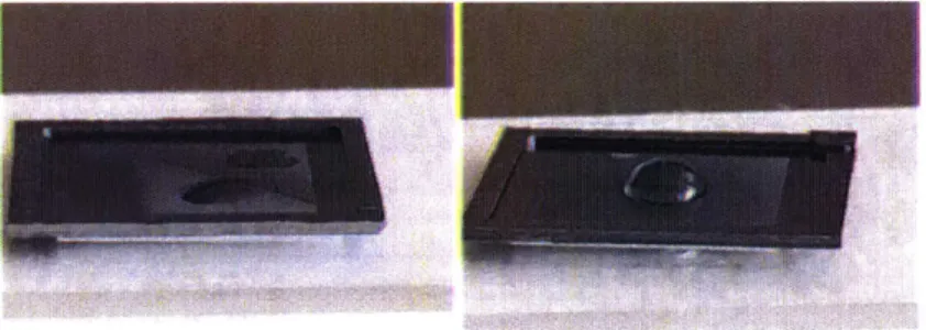
Figure 22: Left: a coated valve and right: a coated valve. The coated valve has a noticeably higher contact angle.
lonic
liquid
Power
IValve
supply
...
Filter paper
Figure 23: Setup for preliminary valve tests.
valve is effectively tunable by altering the coating. Unfortunately, after approximately five days, the coating failed to prevent the liquid from eventually wetting through the valve, necessitating either a thicker coating or an additional layer of treatment.
Next, the ability of the valve to actually work as intended was tested. A thin copper wire was attached to the side of the die (note that by dicing the oxidized wafer, the un-oxidized sides were exposed) and the assembly was placed in good contact with another piece of glass microfiber. A drop of ionic liquid was placed onto the grid and a second wire added such that it was contacting the liquid. The two wires were then attached to a high-voltage power supply. By slowly increasing the voltage, it can then be determined if and when the liquid was forced to wet the capillaries.
As can be seen in the two images below, which are stills taken from a video of the test, the contact angle changes drastically once the voltage reaches a critical point; in this
Figure 24: The setup of the valve duration test. There is a small piece of glass filter paper placed above and below, and the top is saturated with ionic liquid. This is six months after the ionic liquid was first added; it can be seen that the contact angle of the drop in the bottom left corner is still high.
configuration, that point is approximately 30 - 100V. Fortuitously, this is well below the operation potential of the thruster, which is approximately 800 - 1000V.
5.3.2 Robustness
5.3.3 Revised design
While the preliminary design was successful in demonstrating the principal, it also highlighted several issues that needed to be rectified. Firstly, as mentioned, the valve eventually allowed liquid through after roughly five days, failing the passive robustness criteria. The simple solution to this was to adjust the amount of fluoropolymer that was deposited onto the substrate. Interestingly enough, it transpired that there was an optimal level and "more is more" was very much not the case, as demonstrated by the fact that upon testing a valve with approximately 1 lim of fluoropolymer, the liquid immediately wetted through the valve, where it had previously taken several days with only 100 nm. Trial and error suggested that 500 nm is robust and extremely hydrophobic. The additional measure of coating the valve from both sides was also taken, to ensure that the capillaries were well coated. After making this change, in a long-duration passive test, the valve has remained un-breached and the contact angle of a bead of ionic liquid has remained above 900 for more than 60 days.
1783 2019104126 1512HMMD102x2 5k 30 pm 1784 2019/04/26 15-19 H MMD7 8 x4 Ok 20 pm
Figure 25: Valve lip used to pin liquid. Left: Oxide damaged by isotropic over-etch. Right: Undamged lip; note the difference in scale.
or "lip" should be added, the methodology of which will further discussed with the manufacturing. Since liquids exhibit a phenomenon in which the meniscus becomes "pinned" at a sharp corner and they have difficulty negotiating around it, this serves as an additional method by which premature wetting of the capillaries can be prevented.
Thirdly, for ease of attaching a wire, it was decided that it would be necessary to coat one edge in metal (metallization). Through testing different materials, it was determined that a sputtered silver coating was the simplest to solder to, but this must be coated over a thin layer of titanium, which promotes adhesion. To perform this coating without contamination of the valve surface, a simple jig consisting of a Teflon block with milled grooves in which the valves can sit was made -fortunately, while it is difficult to find a mill bit that will allow for cutting a 6 mm deep channel only 0.5 mn wide, a standard 3/16 in bit allows for stacking three valves atop one another. This allows for just the single edge of each valve to be exposed; as sputter coating, by its na-ture, is highly directional, this results in the coating of just that edge and nothing else.
5.4
Valve development
As will be discussed more fully, it was decided that it was necessary to test the valves in isolation first. To achieve this, they will be tested on a specially designed board in space, using hardware that closely resembles the thruster packaging. This served to
Figure 26: The sputtering jig with valves, after metallization. There is kapton tape to help shield the face of the valves.
inform and refine the valve designs to their final state.
5.5
Metal diaphragm valve
In this valve, a membrane is used to isolate the liquid from the emitter chip until such time as it is ready to be fired. The membrane is then damaged to allow liquid to flow through; this design consists of a thin metal diaphragm made of a low-temperature al-loy that may be readily melted by an embedded insulated heating wire. Once molten, a hole should form and allow liquid to flow through. The specific combination used here was anm alloy of bismuth, tin, cadmium and lead, so chosen due to its high vapor pressure; initially, it was intended that the metal would be deposited via thermal evap-oration over a grating. While this did not work as intended, nevertheless the metal is suitable for this function due to its malleability, and thus ease of forming, in addition to its low melting point.
To assist in the formation of a hole in the molten membrane, a thin nitinol (a nickel-titanium shape memory alloy) was coiled and bonded to the membrane in three spots