A Clamped Folded Cascode Amplifier for
Analog-to-Digital Converter Applications
by
Allison Margaret Marino
Submitted to the Department of Electrical Engineering and Computer Science in partial fulfillment of the requirements for the degrees of
Bachelor of Science and
Master of Science at the
MASSACHUSETTS INSTITUTE OF TECHNOLOGY
May 1994
()Allison Margaret reproduce and to
Marino, 1994. The author hereby grants to MIT permission to distribute copies of this thesis document in whole or in part.
Author
...
Department of Electrical Engineering and Computer Science
May 1994 Certified by ...-/ , I
Certified
by...
Accepted
by...
James K. Roberge MIT Thesis Advisor'"~/ ....
lliam T. Mayweather,
III
Company Supervisor
....
* *B* rn
--
X-**...
...
Ch CaDepayentCmiteo Dep
a
Committee rdaeSueton F.G raduat StudentshalereA Clamped Folded Cascode Amplifier for Analog-to-Digital
Converter Applications
by
Allison Margaret Marino
Submitted to the Department of Electrical Engineering and Computer Science on May 1994, in partial fulfillment of the
requirements for the degrees of Bachelor of Science
and
Master of Science
Abstract
The performance demands on analog-to-digital converters for high speed, high accu-racy, low power, and small die area are continuously increasing. Overdrive recovery time of the comparator is a speed-limiting factor in high bit accuracy successive ap-proximation analog-to-digital converters. The bottleneck is most severe when a large input is followed by a small input of the opposite polarity. Output clamping is one way of improving overdrive recovery time. A single stage, folded cascode amplifier with clamping and auto-zeroing is presented. Active clamping is explored in detail and an auto-zeroing scheme is presented for a 12 bit analog-to-digital converter in a 0.8 micron technology. The optimized clamped folded cascode amplifier is then compared with existing comparator gain stages.
MIT Thesis Advisor: James K. Roberge
Acknowledgments
I would like to thank the members of the Systems and Integrated Circuit Design group at the David Sarnoff Research Center for always being available for technical support,
and for making me feel at home at the David Sarnoff Research Center. I particularly appreciated Don Sauer's critical technical guidance, and Bill Mayweather's efforts to get me the resources I needed and keep me on schedule. I would also like to thank Professor Roberge for always responding quickly to my calls and questions, even though I was not on campus.
Contents
1 Introduction
1.1 Motivation ... 1.2 Background ...
1.2.1 Sequential Successive Approximation ADC 1.2.2 The Comparator ... 1.3 Simulation Environment ... 1.4 Outline. ... . . . . . . . . Architecture . . . . . . . . . . . .
2 The Non-Clamped Folded Cascode
2.1 Introduction ... 2.2 Device Modeling ... 2.3 Folded Cascode Gain ... 2.4 Output Capacitance ... 2.5 Transient Analysis ... 2.6 Biasing. ...
3 The Clamped Folded Cascode
3.1 Introduction ...
3.1.1 Passive Clamping ... 3.1.2 Active Clamping ...
3.2 Active Clamping Simulation Implementation 3.3 Clamping and Gain ...
3.4 Effect of Clamping on Output Capacitance .
10 10 11 11 11 12 12 13 . . . 13 . . . 13 . . . 15 . . . 19 . . . 20 . . . 21 22
...
22
...
22
...
23
...
24
...
25
...
27
. . . . . . . . . . . . . . . . . . . . . . . .3.5 Discharge Current ...
3.5.1 Resistance of the Clamp 3.5.2 Clamp Time Constant . 3.6 Clock Feedthrough ...
3.7 Clamp and Input Timing .... 3.8 Clamp Sizing ...
4 Autozeroing
4.1 Introduction ... 4.2 Approach ...
4.2.1 Background ... 4.2.2 Referred Input Offset 4.3 Simulation Results ...
4.3.1 Normal Operation 4.3.2 Mismatch Operation 4.4 Autozeroing Summary . . .
5 Comparison and Conclusions
5.1 Review ...
5.2 Impact of Improved Overdrive Recovery Time on Sampling Rate 5.3 Comparison to Multistage Amplifier ...
5.4 Conclusion: Single Stage Versus Multistage Comparators ....
27 28 28 30 31 32 33 . . . 33 . . . 33 . . . 33 . . . 34 . . . 34 . . . 34 . . . 35 . . . 35 37 37 37 38 39
...
...
...
...
...
...
. . . . . . . . . . . . . . . . . . . . . . . . . . . . . .List of Figures
2-1 2-2 2-3 2-4 2-5 2-6 2-7Low Frequency Small Signal Model ... Complete Small Signal Model ...
Fully Differential Folded Cascode Circuit . . . Half Circuit for Small-Signal Gain Calculation Norton Equivalent Circuit ...
Circuit for IShortCkt Calculation ... Circuit for Ro,,p Calculation ...
3-1 Passive Clamp ...
3-2 Referenced Active Clamp ...
3-3 Single Stage High Gain Clamped Amplifier Transient . . 3-4 Clamping Circuit Representation ...
3-5 Clamping Circuit Representation with Differential Drive 3-6 Clock Feedthrough Circuit ...
4-1 Autozeroing Technique ... . . . 14 . . . 15 . . . 16 . . . 17 . . . 17 . . . 17 . . . 18 23 24 25 29 29 31 36
List of Schematics
Schematic A: Unclamped Folded Cascode Amplifier ... 41 Schematic B: Clamped Folded Cascode Amplifier ... 42 Schematic C: Autozeroed, Clamped Folded Cascode Amplifier ... 43
List of Simulations
Simulation Simulation Simulation Simulation Simulation Simulation Simulation SimulationA: Unclamped Folded Cascode Transient ... B: Clamped Folded Cascode Transient ... C: Clamping Time Constant ... D: Effect of Input Timing on Output ... E: Differential Clock Feedthrough ... F: Pronounced Clock Feedthrough ... G: Autozero Functioning without Mismatch ... H: Autozero Functioning with Mismatch ...
45 46 47 48 49 50 51 52
List of Appendices
Appendix A: SPICE Modelfile ... 53 Appendix B: SPICE Parameter Explanation ... 55 Appendix C: DC Operating Point ... 59
Chapter
1
Introduction
1.1 Motivation
Applications for high speed comparators in analog-to-digital converters (ADC's) range from High Definition Television to ultrasound imaging. Because the world is inher-ently analog, there will always be a need for faster and better ADC's to keep pace with the newest digital processing circuitry.
At the heart of analog to digital conversion is the comparator. The comparator is frequently the speed limiting factor in high bit accuracy ADC's. Overdrive recovery
time is often the cause of speed loss. For example, in a 12 bit converter with a 2V input range, the comparator must be able to sense and amplify voltages ranging from under 0.49mV (an LSB) to a full scale 2V. Without careful comparator design, overdrive will inevitably occur and prevent accuracy at a high sampling rate.
The issue of overdrive recovery has not been thoroughly examined for folded cas-code amplifiers with respect to clamping. Improving the overdrive performance for a folded cascode amplifier, using a non-cascoded amplifier as a reference, is an interest-ing and challenginterest-ing technical problem.
1.2 Background
1.2.1
Sequential Successive Approximation ADC
Architec-ture
In the sequential successive approximation (SSA) architecture, the ADC input voltage is successively compared to binary weighted voltages. The value compared to the input signal in each successive cycle is based on the outcome of the previous cycle. For an N bit converter, the digital output will be available after N clock cycles. Because the SSA architecture requires only one comparator, it is efficient in terms of die area consumption. For reference, an N bit flash type ADC requires 2N comparators. A
flash architecture works by simultaneously comparing each possible input level to the actual input voltage. For high bit accuracy converters, a full flash structure is impractical, while an SSA type remains perfectly reasonable. For more general information on ADC's, refer to [15] or [8].
To increase the throughput of an SSA converter, the comparator may be du-plicated. If N comparators are used, the converter can simultaneously process N inputs,resulting in an N cycle latency and a throughput of 1 output per cycle. Addi-tional cycles for autozeroing or error-correction may increase the latency.
1.2.2 The Comparator
A comparator is comprised of a gain stage and a latch (usually regenerative) for converting the output of the amplifier to a digital level. The amplifier explored in this thesis is designed for an existing latch used in other ADC designs at the David Sarnoff Research Center. This latch has a worst case input offset voltage of 5mV. This offset voltage is large because input accuracy has been traded for lower power consumption. The Sarnoff latch consumes approximately mW of power and converts an input of 5mV to a digital level in approximately 1.5ns.
Because the comparator is destined for large digital integrated circuits, a fully dif-ferential design is required to satisfy noise immunity constraints. Ease of manufacture
is also important; consequently it is assumed that no laser trimming or specialized devices, such as Schottky or high frequency diodes, are available.
1.3 Simulation Environment
To verify and improve the theoretical comparator design, Mentor Graphics Falcon Framework, Design Architect schematic editor, and Accusim simulator were used for simulations. The technology simulated was a 0.8 micron, 5V, double metal, N-well process. The SPICE modelfile was developed from measurements taken on previously fabricated chips from the vendor. Representative SPICE models are included in
Appendix A.
1.4
Outline
Chapter 2 clarifies the fundamentals of the folded cascode, such as gain, parasitic output capacitance, and biasing. The MOS device models used are also included.
Chapter 3 examines passive and active clamping for the folded cascode amplifier. Clamping theory is developed, and related problems are addressed.
Chapter 4 explains the autozeroing circuitry. This circuitry is important because a large input referred offset due to sizing mismatch or threshold variations is anticipated.
Chapter 5 compares David Sarnoff's existing 12 bit non-cascoded multistage am-plifier with the clamped folded cascode. The evaluation metric is speed. Conclusions
Chapter 2
The Non-Clamped Folded
Cascode
2.1 Introduction
A folded cascode architecture has the potential for very high gain, with more output swing than a non-folded cascode. As a result, the folded cascode is useful not only in the 5V technology being used for the simulations in this thesis, but also in 3V processes. An additional benefit of a cascoded design is the small back coupling from the outputs to the inputs.
In the following sections, the theoretical gain, capacitive loading, unclamped over-drive recovery time, transient response, and biasing of the folded cascode amplifier are explained. Equations are developed to enable easy modification of the folded cascode's characteristics via device sizing.
2.2 Device Modeling
The low frequency small signal transistor model used to characterize the folded cas-code is shown in Figure 2-1. Equations defining the transconductance, source-drain resistance, and quiescent current are as follows:
r - 1 _ 1 ° kAID go where ID = IC" - (VGS - Vt)2, when VDS > VGS - Vt > 0; tCo L (VGs - Vt) VDS - VDS] when (VGS - Vt) > VDS > 0; 0, when VGS < Vt.
Appendix B explains the variables in the equations and models, and relates them to the SPICE model parameters in Appendix A.
A complete MOS device model is shown in Figure 2-2. The capacitances were considered open circuits for the gain calculations. The backgate transconductance,
gmb, did not have a large impact on the gain (at most a few percent) and was thus
ignored for the gain calculation.
D
G
Ii
S S G D DG
Vv gs S D I 0 g v r m gs oC S~~~- b S-b bdb
T
1
gb
S
T
sb
T
db
BB
Figure 2-2: Complete Small Signal Model
2.3 Folded Cascode Gain
The fully differential folded cascode circuit is shown in Figure 2-3. A half circuit, shown in Figure 2-4, is used to calculate the small signal gain. In the half circuit, the resistances of M1 and M3 have been represented by ri, which equals r 1l1ro2.
Assuming no mismatch, the complete differential gain is equal to the half circuit gain. The impact of mismatch on circuit performance is addressed in more detail in
Chapter 4.
The common node is grounded in the half circuit because any change in voltage on that node would be reflected as common mode gain, and thus would have no impact on the differential gain. For further discussion on the common node virtual grounding approach, refer to [14, pages 255-257 ].
A Norton equivalent circuit approach is used to calculate the gain of the half cir-cuit. In a Norton equivalent circuit, shown in 2-5, the behavior of a more topologically complex circuit is exactly modelled as a current source and resistor in parallel.
Figure 2-6 shows the circuit used to determine the short circuit current. Figure 2-7 shows the circuit used to calculate the equivalent resistance.
vdd M3 ml I - A, ,q Vrn -Vb as2 vout -Vb as I I Vblas 1
Figure 2-3: Fully Differential Folded Cascode Circuit
V n+
q g9
out
-g 7V-gs, r7
Figure 2-4: Half Circuit for Small-Signal Gain Calculation
'Short
Ckt4.
Vout
Figure 2-5: Norton Equivalent Circuit
Vn+ gnlVin+ r, n (S Ms vgsC5
l
4X~sc
Figure 2-6: Circuit for IShoitCkt Calculation
+ V s · ! %~~~~~~~~~~ l I ! . 5 V 7
I t est
+
K
+b
Vt est 9MsVoss o voQs s
_b
]~N-4¥
Figure 2-7: Circuit for Ro,up Calculation
The short circuit current is calculated as follows:
ISc = 9mSVgs5 + Vgss5/ro5 - -gmlVin - Vgs5/rin
-Vin~ml
vgs5 =
VSC = Vin5
(
gm+go i min(g.m9+gor,+go,in) g l)
In order to calculate Rout RoUp and Ro,dovm must also be calculated. The gm's and ro's specified in Figure 2-7 are for Roup as noted in Figure 2-4. Roup is calculated
as follows:
Itet
= gm5sVg,5 + vtet+Vg5 = -vg5/rivg.5(gm5 + go5 + go,in) = -Vtestgo5
Vteatgosgoin Itest - (s5 +go5 +go,in)
//,p= Vtat /test D YZ
I
-= (g'_+g°__+go,__Sm6go5 go,jinoRu =Viestl test -:::: (go+gor,inj
Since Ro,down has an identical topology:
-o~o~.~ =(gm7+9o+g7)
Rosdown - gOm1+9g+9,
go7go9
Thus,
Rout = Ro,dow
ilRoup
If the transistors are in the saturation region (when Vd. > (Vg, - Vt)), then it can be assumed that g << gn, such that the expressions for IShortCkt and Rout simplify to:
ISC =-Vingml
Ro t= ( Gn )1I( g-
Putting the two results together, the total gain is
,ur+ -vou *- gm[ ) 9- )]
vin+ -vin- - gmi K 9.ogo,-n go7go9
For the circuit shown in Schematic A, the simulated DC gain is 880. For a 12 bit converter, in dc operation such a gain will amplify half an LSB (.24mV) to 4 times the latch offset voltage.
Transistors M9A and M1OA in Schematic A are used in the autozeroing circuitry and can be temporarily ignored for the gain calculation. The device sizing shown results in quiescent currents of approximately 100/tA in each transistor, which yields
a transconductance value of:
gml = .92mS
Drain-source conductance is difficult to accurately hand-calculate, so the simulator was used to determine the exact gain. Working backwards from the calculated gml and the simulated gain gives a value of Rout = 0.96MQ. Appendix C contains dc operating points for the folded cascode, and Appendix B contains the equations used to generate gmi. It is important to have a estimate of Rout for speed considerations because the dominant time constant for a folded cascode amplifier is due to the output loading.
2.4 Output Capacitance
Just as an accurate output resistance value is important, an output capacitance value is necessary to predict the circuit's behavior. The following equation models the capacitive loading at the negative output terminal:
If M5 and M7 are in saturation:
Cload = Cdb,5 + Cgd,5 + Cdb,7 + Cgd,7 + Cmisc.
Appendix B gives equations for drain-to-bulk and gate-to-drain capacitances.
Cmisc represents the miscellaneous loading due to any following stages and the
un-modeled parasitic capacitance from the wiring.
It is important to note that the drain-to-bulk and gate-to-drain capacitances vary proportionally with W. To avoid unnecessary loading, the width of devices M5, M6,
M7, and M8 should be kept as small as possible. At equilibrium (when Vot- = Vout+ = 2.5V), for the device sizes shown in Schematic A,
Cgd,7 0.47fF
Cdb,7
3.4f F
Cgd,5 = .84fF
Cdb,5 = 6.8fF
With an estimated value of 10fF for CmisC this gives a value of Cload = 21.5fF.
2.5 Transient Analysis
The worst case overdrive recovery time occurs when a large input is followed by an LSB input of the opposite polarity. Assuming temporarily that the output equilibrium occurs at Vo0 t- = Vot+= OV, Vo0 t_(t) can be modeled as follows for a positive LSB following a negative MSB:
Vout-,O, -2.5 volts
VoIt(t) = [-2.5e + 0.22(1 - e )] volts, t > 0
The first term of Vot- is a decaying exponential due to the state created by the negative MSB; this term exists until Vot- passes through 0 volts. The second term is a rising exponential caused by the new input. The 0.22V final voltage is the result of multiplying the gain (880) by half of an LSB (0.24mV for an input voltage swing of 2V). The value of half of an LSB is used because the circuit is fully differential, and the other half of the circuit is operating in exactly the same way, but with the opposite polarity. The dominant time constant is due to the output load, where
r = RoutCload
=
(960KQ)(21.5fF) 21ns for the circuit shown in Schematic A.By solving for t when Vot- = 25mV, the time it takes to reach the latch offset of 50mV (assuming Vt+ is undergoing similar changes in the opposite direction), the maximum comparison time necessary to trigger the latch can be found. For the values mentioned above, it theoretically takes 52ns to reach a differential output of OV and 2.5ns more to reach a 50mV differential output. The total theoretical comparison time is thus 54.5ns. Simulation A shows the actual unclamped folded cascode transient
response for this case. The simulated time from the new input to the 50mV necessary for latching was measured as 57ns, just 2.5ns off of the predicted value. The extra delay is probably due to the changing gate-to-drain and drain-to-bulk capacitances, but could also be the result of a slight error in the estimate of
Rout.
2.6 Biasing
The biasing scheme, consisting of transistors M12, M13, M14, and M15 as shown in Schematic A, consists of 4 diode connected transistors. It was chosen for its simplicity and lack of fixed voltage requirements. The current in the bias leg of the transistor is approximately 10 A. This current is mirrored and scaled up to - 100,uA in all transistors except M9A, M1OA, M3, M4, and Mll. Transistors M9A and M1OA have smaller currents than the other devices because they are for output level adjustment only; M9 and M10 carry most of the current in the parallel combination. M3, M4, and Mll have currents of approximately 200 A. IM7 and IM8 were set slightly larger than IMl and IM2 to avoid a situation where there is not enough current to meet the demands of the input transistors.
Chapter 3
The Clamped Folded Cascode
3.1 Introduction
The goal of clamping the outputs of an amplifier is to limit the differential output voltage as quickly as possible. The unclamped 12 bit overdrive recovery time discussed in Chapter 2 is unacceptable for high frequency applications. This chapter explores how to most effectively clamp a folded cascode amplifier to drive a regenerative latch with a 5mV worst case input offset.
MOS devices are used as the clamping devices because Schottky diodes and good high frequency diodes are not available.
3.1.1
Passive Clamping
Passive clamping is accomplished by connecting the outputs of an amplifier to the source and drain of a MOSFET (or the terminals of a complementary pair of MOS-FETS's). The gate of the MOS device is tied to a fixed voltage.
Passive clamping is easier to implement than active clamping in that it requires minimal layout complexity and is not subject to any clock feedthrough. A viable passive clamp is shown in Figure 3-1, where Vd, is a fixed voltage (5V in most applications).
speed improvements are difficult to predict because MOS thresholds and saturation
Vds are not sharply defined. A MOSFET threshold voltage is dependent on the terminal voltages and doping, which can vary widely on a single chip.
V dc
I
V V
out+
out-Figure 3-1: Passive Clamp
3.1.2 Active Clamping
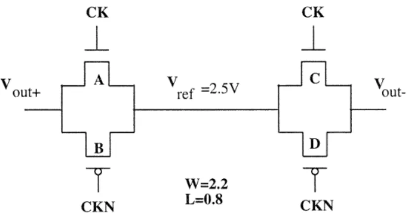
In active clamping, the clamp gate voltage is driven by a clock, and can be with reference to a fixed voltage, as shown in Figure 3-2. However, the clamp does not have to be referenced to anything; it can simply connect two active nodes directly, as in the passive clamp Figure 3-1. If the swing on each output node is very large, a fixed voltage reference is preferable so that a charge equilibrium is reached not far from the nominal output equilibrium value. For a circuit with a large output swing, complementary transmission gates are needed to effectively clamp at both the positive and negative rails. Additionally, complementary transmission gates also partially cancel clock feedthrough.
Active clamping is more effective than passive clamping because the active clock ensures the clamp will be turned on at a certain time. The remainder of this chapter focuses on modeling and optimizing active clamping. The most challenging issues involve clock feedthrough and input timing with reference to the clamp.
CK CK
I
I
Vo01
lut-T
W=2.2
T
CKN L=0.8 CKN
Figure 3-2: Referenced Active Clamp
3.2 Active Clamping Simulation Implementation
Due to the limitations of the SPICE model, the clamping scheme shown in Schematic B had to be used. The clamp network consists of 4 transmission gates (devices MC1-MC8) referenced to 2.5V (labelled Vfis). While only two transmission gates would be needed in a physical implementation, a software bug necessitated simulating with 4 to get accurate drain and source modeling. (Otherwise, the simulator yielded different results depending on the nominal location of the drain in the schematic.) This fix caused the parasitic capacitance to be non-symmetric for the devices and threw off the capacitive coupling by an unrealistic amount. By placing two devices of half the nom-inal width of 2.2pum in parallel with opposite drain locations, the simulator limitations were overcome. The only major problem caused by the alternate simulation imple-mentation was an increase in the source-to-bulk and drain-to-bulk capacitances due to apparent sidewall and junction parasitic capacitances. This error is compounded by the fact that a software designer implemented the default sidewall capacitance to
be proportional to 2W + 2Ld, not W + 2Ld as is correct and as shown in Appendix B. The net effect is extra capacitive loading at the output, and slightly more clock feedthrough. Though the simulation correlation to the physical design is non-ideal, the result is tolerable because the additional capacitance (at most a few fF) effectively substitutes for the parasitic capacitance due to wiring that was not included in the simulation model. For clarity of discussion, the rest of the sections in this chapter reference the clamping scheme shown in Figure 3-2. Predicted capacitance values will be based on the device sizes shown in Figure 3-2, but the values corresponding to the actual implementation will be indicated when there is a noticeable discrepancy.
V
Vfinal
! I I /t
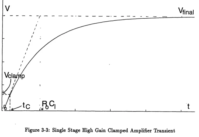
Figure 3-3: Single Stage High Gain Clamped Amplifier Transient
3.3 Clamping and Gain
In Figure 3-3, to represents the time from zero seconds to the time the output has moved enough to be latched, and is thus ready to be clamped. The dominant time constant RCl is due to the output loading. Voltage Vfi,~ is the product of the
smallest input that must be recognized and the gain of the amplifier. Voltage Vc is the minimum value necessary to trigger the latch correctly. If it is assumed that:
VC < < Vf inal tc reduces to A
Substituting r = RLCI and Vf = gRLVmin yields:
C gmVmn
Thus, to minimize t, gm, should be increased. This is the sensible result, since increasing power usually increases speed. The result indicates that the specific gain of the clamped folded cascode does not matter, as long as it is high enough such that
Vc << Vfinal. Figure 3-3 assumes an ideal clamp and does not account for clock
feedthrough.
Substituting Cl = 32fF (calculated in the next section), Vc = 50mV, g = .92mS, and Vmin = 0.49mV results in t = 3.5ns. Simulation B shows (from top to bottom) a plot of the clamp, the differential input voltage, and the differential output voltage. From the time the clamp releases, it takes 5ns for the output to reach Vc when driven by an LSB after an MSB of the opposite polarity. Part of the 1.5ns discrepancy between theoretical and measured time delay can be attributed to the gm 1 calculation in Chapter 2. An alternate way of calculating gmin is to work backwards from the 3dB point of the clamped folded cascode and the output load, assuming a single dominant pole. The corresponding output resistance for f3dB = 4.67MHz
(from simulation data) and C = 32fF (theoretical) is 1.07Mg. Working backward from the theoretical gain of gmlRout, the simulated gain of 880, and the new value of 1.07MQ for Rout yields a gm1 of 0.83mS. Substituting this gm into the t equation yields a delay of 4ns, closer to the simulated value. The remaining discrepancy can
be partially accounted for by the extra capacitance introduced by the artificial 8 transistor clamp implementation.
3.4 Effect of Clamping on Output Capacitance
Adding MOS clamps to the outputs of the amplifier increases the total capacitive load. Assuming Vot- << 2.5V, the following additional capacitive components will be present at output node Vo,,t- when the clamp is turned on:
CgdB + CdbB + CgsA + C,bA
At Vout+:
CgdD + CdbD + Cg.c + Cs.bC
Referring to Appendices A and B, and using bias points of Vdb = 2.5V, Vsb = 2.5V, with sizing of W = 2.2, Lnmos = .645, and Lpmos = .674
ACload-
=10.5fF
ACload+ = 10.3fF
Cload = Cload,unclamped + A Cload -
32fF
The actual simulation transistors result in equal AC loads of 13.2fF, which slow down the circuit a little.
3.5 Discharge Current
Discharge current (the current going through the clamp) determines how quickly the clamp can minimize the difference in the outputs. When determining how long the clamp should be on, a model is helpful. It is possible to model the clamp as a resistor, but the value of the resistor changes so unpredictably that the model is only helpful for general trends or when focusing on an operating point.
At any given time the clamp is on, both devices are operating in the linear region, one with a fixed gate-source voltage, and one with a gate-source voltage that varies with the output voltage. If the output is greater than 2.5V (the voltage the clamp is referenced to), the N device has a fixed gate-source drive. If the output is less than 2.5V, it is the P device that has a fixed drive.
3.5.1
Resistance of the Clamp
If the VDS term is dropped from the following linear region equation: ID = ACO [(Vg - Vt)VDS VD]
The fixed drive device can be modelled as a resistor of value
RC = _O Lg1
Mobility t is dependent on Vd,, such that the value of this Rc, decreases nonlin-early with Vds.
The non-fixed drive device behaves according to the linear region equation noted for the fixed drive device, but the resistance of the non-fixed drive device increases nonlinearly with VDS. This is because the net effect of the gate-source voltage de-creasing outweighs the changing mobility.
The total clamp resistance is equal to the parallel combination of the resistances of the two devices.
3.5.2
Clamp Time Constant
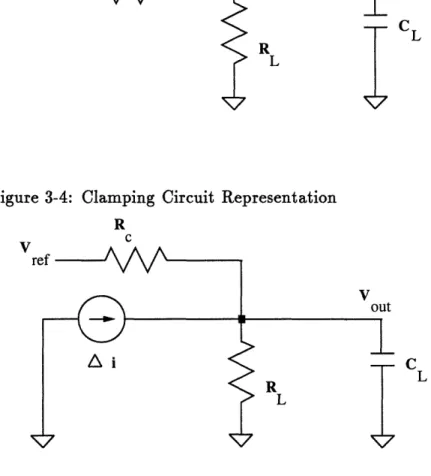
Considering the clamp to be a variable valued resistor, the entire circuit can be approximated by the circuit shown in Figure 3-4.
The following equation shows the transient response:
-t(1/RC+l/RL)
V. . R-
(1 -e
CL)
RC+RL
Simulation C shows the change in outputs in response to the clamp turning on. Within the first 2ns the clamp is on, the outputs are drawn from a full differential output to within 0.3V of each other. After that, the clamping dramatically slows down. The clamp transient response equation is difficult to match up to the simu-lations and of questionable value. Nonetheless, the resistive modeling aspect of the transient equation (the final dc response) is important to note.
The equation does reveal that because the load is not purely capacitive, the final value due to clamping alone is not equal to the reference voltage, but a large fraction of it. It is also important to recognize what an input drive does to the output voltage. Such an input drive could be due to mismatch within the circuit or to an actual signal
at the input of the amplifier. For the model shown in Figure 3-5, where Ai = gmii, the final value output voltage is
Vo.t = AiRc + Vi,
assuming RL
>>
Rc Simulation D illustrates this effect. Though the clamp turns on at 42ns, 0.5V is maintained across the outputs until the drive on the input is removed. The input is removed at 45ns, at which point the differential voltage starts to decay.R c V V out ref R L ref
V~~~~~~~~~~~out
L
CL
Figure 3-4: Clamping Circuit Representation R
C
R L
3.6
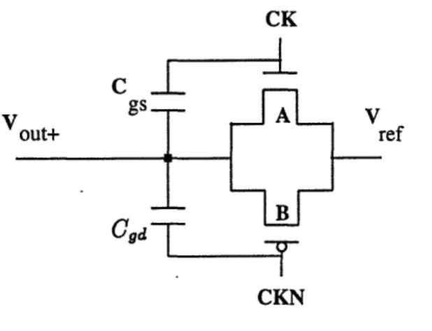
Clock Feedthrough
The output voltages are directly affected by the clock transitions via coupling to the clock, or feedthrough, as shown in Figure 3-6. The complementary devices partially cancel each other out, but not entirely; complete cancellation can never be depended on because process variations inevitably create some mismatch among coupling capacitors.
If the output voltage is less than 2.5V, then the NMOS device will couple to the output via Cg8 and the PMOS device will couple to the output via Cgd. For the
clamp sizing shown in Figure 3-2, CgA = 2.46fF and CgdB = 1.83fF. The following equation characterizes the coupling effect:
Vout- = C Cd gd + C C = 98mV
-- Cgd+Czoa.d Jc Cgo+Clo.d
For Vot+, which has slightly different loading conditions, the net clock coupling results in approximately 84mV. Thus the differential coupling effect comes to about
14mV.
Simulation C shows both outputs after being clamped for 20ns. No new input is applied after an MSB input the cycle before. Both outputs drop by approximately
110mV, on the order of the predicted 98mV and 84mV. In the waveform at the bottom of the page in Simulation E, it is possible to see the differential coupling effect when the clamp is released at 54ns. With no new input, the differential output jumps approximately 12mV when the clamp is released and can be seen to decay thereafter.
Simulation F shows a close-up of what happens when the outputs do not reach the reference voltage. The PMOS and NMOS gate-to-drain and source-to-drain ca-pacitances are not as well matched and the common mode coupling doesn't cancel as well as in Simulation E, resulting in a common mode output drop of 0.35V. It can be inferred that if the two output voltages are not close to each other they will not couple uniformly, which could result in a large differential voltage change. Clamp input timing is important in preventing such a situation.
CK
C~~~~~~~~
V gs~~-- V
out+
ref
CgdT
'
T
CKNFigure 3-6: Clock Feedthrough Circuit
3.7 Clamp and Input Timing
The only major input timing constraint is that the last output be removed before the clamp turns on or very soon after it turns on. This is crucial for the case of a large input followed by a small input of the opposite polarity, as is evident from Simulation D. The large input prevents the outputs from getting close to each other. If the differential output is not lowered before the clamp ends, an LSB of the opposite polarity will not be strong enough to discharge the outputs quickly.
Introducing the new input while the clamp was still on yielded the lowest time from input turning on to output reaching the latch offset voltage. This time, shown in Simulation B was 7.5 ns. The input was applied for 2.5ns before the clamp was released. It took 5ns to reach the valid latch voltage after that. When the new input was not turned on until after the clamp was off, the time delay was approximately
3.8
Clamp Sizing
Both the P and N clamping devices need to be sized equally so that clock feedthrough will be minimized. Larger W ratios decrease the clamp resistance, but increase the
capacitive loading. Whether increasing the clamp size has a positive or negative effect on the speed of the circuit depends on the SPICE parameters and the default layout parameters. For the SPICE model used in this thesis, increasing the clamp size was not effective. Doubling the clamp width to 4.4 /im resulted in a 3 ns increase in the time for the outputs to reach 50mV.
Chapter 4
Autozeroing
4.1 Introduction
Autozeroing, or autobalancing, is the cancelling of any dc offset on the output nodes, such that the input referred offset is very small. There are two basic approaches that can be taken to cancel these offsets. One is to feedback via a switched capacitor network a fraction of the output such that each output is compensated independently, but with respect to the same fixed voltage. Another technique is to cancel the common mode and differential mode with two separate feedback loops. The former approach was chosen because it allowed for hysteresis and non-correlation between the two legs of the cascode, without the need for aggressive sizing techniques.
4.2
Approach
4.2.1
Background
Figure 4-1 shows the basic feedback concept, consisting of a switched capacitor low pass filter and a single ended differential amplifier for each output. If process inac-curacies cause an output to be too high, a high voltage is fed back to the parallel feedback device, causing its resistance to drop and thus the output voltage to drop also. The single ended differential amplifier, consisting of devices M16-M20, is
refer-enced to 2.5V; and its equilibrium output is centered at 2.5V. The nominal feedback voltage to M9A and M1OA is centered at 2.5V to produce the nominal folded cascode output of 2.5V. The actual feedback circuit implementation is shown in Schematic C.
4.2.2
Referred Input Offset
To avoid large output swings due to the feedback circuitry, the change in output voltage due to the maximum possible change in feedback voltage per cycle must be limited to much less than the change in output due to an LSB.
The gain from Vg,M9A to Vote- is, based on the same calculation methods used for the folded cascode gain equation in Chapter 2:
lZt-
--gma
VUt - n -9gmso9Ag = 13, as measured in simulation.
Vg,M9 A gingo5 /g,7b +9o7 909 /g7,
To prevent the output from switching too rapidly, CL2 and CR2 are each 10pF, to be implemented with depletion NMOS devices. CL1 and CR1 are each approxi-mately 4.4fF. With these capacitance values, the maximum feedback voltage swing
is 4VCL = 1.8mV. Amplified by the feedback gain, this results in a maximum
CL2+CL1
-voltage change of 21mV. A 21mV change referred back to the input of the amplifier corresponds to an input of 24/KV, less than one twentieth of an LSB .
The feedback is powerful enough to compensate for large input offsets, but not in one cycle. The scaling down of the feedback capacitors makes the system stable and allows the feedback to work slowly over several cycles.
4.3 Simulation Results
4.3.1
Normal Operation
Simulation G shows the autozeroing circuitry functioning with no mismatch and a default initial condition on Vg9A and VglOA of 2.5V . The key waveform in the Sim-ulation is Vot-, the fourth waveform from the top of the page. It gradually settles to the nominal 2.5V. The intermediate waveforms are shown above Vot- and can be examined more closely by referring to the node names shown in Schematic C,
if desired. The bottom two waveforms show the two stage feedback clocking. The nominal overal period was set at 40ns, though in an actual 12-bit implementation, the total period would be longer because the autozeroing would only occur once per overall ADC timing cycle.
4.3.2 Mismatch Operation
To verify the effectiveness of the autozeroing, various simulations were run with sensi-tive gate lengths changed. The success of the autozeroing circuitry depended heavily on how the feedback timing related to the clamp timing. Simulation H shows the result when both input devices have a nominal gate lenght of 0.85 m instead of 0.8/Lm. The format of the Simulation H plot is just like that of Simulation G. The autozeroing circuitry eventually centers the output around 2.5V.
4.4 Autozeroing Summary
The autozeroing circuitry was pursued to determine if there existed a fundamental problem associated with autozeroing a high gain clamped stage. While no inherent problem was found, it is important to note that this particular autozeroing scheme is not crucial to the clamp's operation, and hasn't been optimized to work with the clamping. Autozeroing issues not discussed at length here include the time constant of the feedback, its interaction with the clamping of the amplifier, and potential feedthrough-related problems.
T
Figure 4-1: Autozeroing Technique
0)
(5
U
)i
Chapter 5
Comparison and Conclusions
5.1
Review
The goal of this project was not to produce the fastest 12 bit ADC possible, but to push the limits of affordable, low-power technology by speeding up one of the critical paths in high bit-accuracy ADC's. The amplifier itself consumes 2.5mW of power (not counting auto-zeroing circuitry), and the rest of the ADC circuitry would consume an estimated 300mW, based on present Sarnoff designs. When compared to amplifiers of this power and technology (CMOS), the clamped folded cascode outperforms them all. However, before making a comparison, it is necessary to relate the clamped time response to the worst case series of inputs to the potential sampling rate of the ADC in which the amplifier will be implemented.
5.2 Impact of Improved Overdrive Recovery Time
on Sampling Rate
As mentioned in chapter one, a pipelined SSA ADC has a fundamental internal
clock-ing frequency that may also be the samplclock-ing rate. While the total period of the multiple phase clock depends on the autozeroing and error correction schemes, the fundamental period is foremost limited by the comparison time, and the delay around
the decoding and subsequent digital-to-analog(DA) conversion for the next cycle com-parison. It would be difficult to run the internal clock any faster than the frequency limit of the comparator-DA loop because the loading of so many comparators on the voltage reference lines would become unmanageable. This means that the overdrive recovery time can directly limit the sampling rate of a high bit accuracy ADC. For a different Sarnoff ADC implemented in ltm CMOS, the delay from the output of the latch to a new valid comparator input is approximately 12ns. With the 0.8/tm technology simulated in this thesis, that time would probably reduce to O10ns without any major topology changes. Thus, the fundamental period limit for the simulated amplifier would be 17.5ns, based on a worst case delay of 7.5ns from valid amplifier input to valid latch input plus a delay of O10ns from latching to valid DAC output.
This converts to an admirable 57MHz sampling rate limit.
5.3 Comparison to Multistage Amplifier
The single stage clamped folded cascode beat an existing 12-bit Sarnoff ADC amplifier under worst case input voltage conditions by approximately 5ns. This two stage clamped amplifier was implemented in l/m CMOS and was clocked (the whole ADC) at a maximum sampling rate of 40MHz. The multistage amplifier drew 4mW of power, more than the clamped folded cascode.
The multistage amplifier, though used for a 12-bit ADC with a 2V input swing, only had to sense a minimum input voltage of lmV, not the 0.49mV the folded cascode was tested at, because of clever input circuitry and amplification prior to the signal's entrance to the comparator. If the clamped folded cascode only needed to sense 2LSB, it could potentially be clocked at 67MHz. However, this would not include much margin for error, just as the 40 MHz sampling rate is pushing the limits of the multistage Sarnoff comparator. It is safe to say that with similar input amplification circuitry, the clamped folded cascode could effectively and reliably perform at 60MHz.
Razavi and Wooley [13] report a 12-bit 5-Msample/s converter implemented in 1[tm CMOS, based on a two-step flash architecture. They too employ clamping, but
require lOOns for input sampling, and an additional lOOns for subsequent conversion. The total power dissipated in both the coarse and fine comparators is 2.25mW, and the overall ADC power consumption is 200mW. While this amplifier consumes slightly less power than the clamped folded cascode, it suffers an order of magnitude decrease in sampling rate limit.
The main delay due to comparison time occurs in the fine comparator, which is a combined amplifier and latch within a folded cascode topology. While some of the sampling rate limit is due to DAC conversion time and logic, a large part of the delay could be elimated if the fine comparator were a clamped amplifier and separate latch.
5.4 Conclusion: Single Stage Versus Multistage
Comparators
Multiple stage unclamped gain stages outperform single stage high gain amplifiers without clamping. This statement is supported theoretically in the standard deriva-tion of the optimal gain per stage of e, as outlined in [4], as well as supported by the reported performance of unclamped multiple stage amplifiers at Sarnoff compared to the unclamped folded cascode. However, it has been shown in this thesis that a clamped single stage high gain amplifier can outperform a clamped multiple stage amplifier. The nonlinearities of clamping and the extra loading due to the actual clamps decrease the potential sampling rate as more stages are added.
The success of the clamped folded cascode amplifier does not have to stop at a 12 bit application. The folded cascode topology has enough gain potential to perform superbly for a 14 bit design as well.
C > 'D iz > I 0
0
7:=0 o S CQ c7v
t~ -4 . . -C. 11 -C'-4 -e0 © -e C. -e: 0 5 -c U (.) c; ·. a6 c > ,
I -4 A S C.) r-w U l) U -eus UC) Cd
u
-tQ) Vsv
S C) To-6 C) C N C C C1) UI,,I - '5 2 0 5 -> 0 w w5 o 0 II I i I I 1l I I I I I I I I I I 1 I I I I I I I I 8 °. m m v m 'It 9 vg o ,- 0 9io (A) 3E)VllOA S S 8 i I § I I I I I I i I . i (A) 3eV.0 A 1 -N I --O - tJ0 Q w -3 4 go -.. v ¢u Uq~ om, ry W q 0 )-- ---.. - s I - .. . . . . -f | | T r -- - - - . 1 . I . . . . I ... I I I I j
> ~ fJ i S a 9 C + UJ Ul -- U5 l I O 0 > o o o n i ll II I IJlli 11 11 I Ij I ll mIIIJ II 11 0 (.-.-- 4-H C, 11 0
4-I11'1 I ..."""11"1 -11... ...-lI .. .... .... J"'J""Ji ' . ......... .
,, N
-N
,;
-
0 0o
8 0 8 0 9 99
9 aO ci ° ° ° ° ° i i i i (A) 3Vl10OA (A) 39V10A (A) 3D91O0A - 4.; U, V 0 0 0 _ -eu -- 00
. m0 'i2 ._ _E V 0 A 0. --- 4 ...-_
I i i i i---r- -- ---i --- - --- - - -- -- - - -]1 i{ IT BL I{ II 111 B] I1 IT 11 IIII]{111111111BIIIIlllll'"l""I..I'"
....
,,^- tt <Y ,^4 _ O _ .^4 .^^. t m X q7 s Ql 4 cM s 5> Y-F :;I-. tu . go. -, cIs. -1, .0 :.9 I I I I -- ' - ' '-1- - '- ' ' ' ' 4 m* ('N (0 0 a,
0
- a. bO0
- 0 (0 -, I -, a; I 8 , , ,; I . . .o . ; . . . . SI . .; o. (A) 3OV110A I I . . . .. - - - - -I ... ... ----I . . . ----I . ----I . . . . mE >
9>
,>>2
L W- N & t-F
o o 0
> > Z
il_ I _ _ lllil ;lIII I I II III I I I I jI III 11111 Ij III
:8 : 8 X 8 , 8 8 O 8 C C .4 ~5 C ~5 C C 8 8 CI C 8
.-(A) DV L OA - (A) 3 " OA - (A) O1 OA (A) 3V110A (A) 3VllOA (A) 3)VllOA
. I -56 10 q -5I Xi 50 N
I-0
0 0 I,.,,-0 .o *_ U) X - - - --- - - - -- - - - - -:... . ... ... ... ... .. - - - T-o
... J] .... II 8 i : Z 5
~
i4 :~5! i~4~i:~;4
~
! : w g K t!8o a c a 8 8c (A) 3DV11OAr
i F I L 0 0 - ,.j0 - I o2 C4 _ -. o.--
I C/3 -! I I--- i tp t1 I ijIi(A) V.'110A (A) 3V1.1OA
8 ---I --- --- m r---- ---I I i II II, ---... ..
=-!
\~~~~~
Lo
bo I _ o I--.o ~~~~~~~~I-·
~~~~~~~
I -7 LIn~~~~~~~~~~~~~~~~~~ (A) 30VI A I
J~~~~~ rX
I--./~~~~~
' F · ~i ' ' i |i ti|ig ~ ' (A) 39V/IOA| U ! W ~ z w W :: w W -. w >^ j; w
o > > O 0 (! Y O -e
I.-
F-o 0 0 0 0 0
> > > > > >
(A) 39VY110A IA) 39V110A
(A) 3VIO0A (A) 39V10A
I II I I I / 11/ 1 8 B , 4 6 cN - 0 (A) 3DV110A I r
l~~~
I-0 t F -09 S 0*A N -0 (A) 39V'1OA u 4.ce0 W bO 0 o I 0 .Z. VO .40 r.3 60 I __j I i I I IIf
~~~~~~~I-
l8 8 8 8 88
Ui t C. N - 0
(A) 39VllOA (A) 39VIOA
(A) 3EV91 (A) 3V1LOA
I i i I -c I C., m 0 ,
-
4 -· _ X .A N - 0 (A) 3E9V110A , . .) 0 ce 0 © .4;
0
bo 0 C,) i P3 ~; e .4 An (A) 3V11OA I I I I I I I I F k 9'''I"1"' _9'"iSPICE MODELFILE
* NMOS L=0.8uM * PMOS L=0.8uM
.MODEL NE NMOS(LEVEL=3 VTO=0.7821 TOX=1.75E-8 RSH=62.5 + NSUB=4.0121E+16 LD=7.7667E-08 UO=480.0
+ VMAX=1.3625E+05 THETA=3.9505E-02 ETA=9.9859E-03 KAPPA=0.1094 + TPG=1 DELTA=0.7667
+ CGSO=4.740E-10 CGDO=1.561E-10 CJ=2.4E-4 CJSW=4.9E-10 + MJ= 0.44 MJSW=0.35 )
.MODEL PE PMOS(LEVEL=3 VTO=-0.9247 TOX=1.7500E-08 RSH=138 + NSUB=4.0116E+15 LD=6.3184E-08 UO=153.4
+ VMAX=1.5801E+05 THETA=8.2588E-02 ETA=3.1827E-03 KAPPA=1.952 + TPG=-1 DELTA=0.5856
+ CGSO=3.718E-10 CGDO=1.6865E-10 CJ=7.1E-4 CJSW=1.87E-10 + MJ= 0.55 MJSW=0.38 )
Appendix B: SPICE Parameter
Explanation
References [5], [1], and [6] contain the equations found in the appendix and can be referred to for further clarification. Variables are listed roughly according to their order of appearance in the text.
Yo( 82)
Channel Mobility
ILff
[~eff -- l+(SoVde)/(Vm=Letft)21+6(Vg-VTH)
Nominal value is given as UO in SPICE model.
Co,(F2): Gate oxide capacitance
toz
Oxide thickness t, is TOX in SPICE. eo is for silicon.
W(um): Channel Width
Nominal channel width is the same as the actual channel width, to a first order approximation.
L(jm): Channel Length
L = Lom -2Ld
On Schematics, the L shown is the nominal gate length. In all equations, L refers to the effective gate length. Length Ld (LD in SPICE) is the overlap due to diffusion on both the drain and source sides of the device.
V(V): Threshold Voltage
Nominal value is VTO in SPICE modelfile. The actual threshold varies with doping and terminal voltages.
Difficult to calculate; depends on device current and gate length.
Cgs(fF): Gate-to-Source Capacitance
In Saturation and Cutoff Regions: gs = WLCo + CGSO W
In Linear Region: Cgs =
CGSO
W + WLCoThe units for the SPICE gate-to-source overlap capacitance CGSO are /lrn2 F
Cgd(f F):
Gate-to-Drain Capacitance
In Saturation and Cutoff Regions: Cgd CGDO W
In Linear Region: Cgd =
CGDO
W + WLCo0The units for the SPICE gate-to-drain overlap capacitance CGDO are /.zyr~2 ·fF
Csb(f F): Source-to-Bulk Capacitance
Under Zero Bias Conditions: Cbo
CJSW. (W
+ 2Lsd) + CJJ.
(WLsd)Biased Conditions: Cb = C0O
V(1 +Vl Vs
The SPICE sidewall capacitance CJSW is in units of fF/tlm. The SPICE bottom junction capacitance is in units of fF/Ium2. Length L d represents the source diffusion
extension beyond the transistor gate. The default SPICE value for b is 0.5V.
Cdb(f F):
Drain-to-Bulk Capacitance
Under Zero Bias Conditions:
Cdbo =CJSW. (W
+ 2Ldd) +CJ.
(WLdd)Biased Conditions: Cdb = C
Length represents the L diffusion extension beyond the transistor gate.)drain Length Ldd represents the drain diffusion extension beyond the transistor gate.
The gate-to-bulk capacitance depends on the extension of the gate area beyond the active channel region, CJSW, and CJ. Area and perimeter values are smaller than for Csb and Cdb so this capcitance was left out of theoretical calculations.
gmb(mS): Back-gate Transconductance
gmb 2 24 f + V bg
7 = C!v2q cNs
The backgate transconductance was ignored for all calculations. The error it introduced was on the order of 2.5 percent. Substrate doping Ns is represented in SPICE by NSUB and measured in units of atoms/cm 2. For silicon, = 1.04e-12F/m. Charge q= 1.6e-19C.
Net/Pin //GND:v //VDD:v /Cl/NEG:i /Cl/POS: i /C2/NEG:i /C2/POS:i /C3/NEG: i /C3/POS:i /C4/NEG:i /C4/POS:i /ckl:v /ckln:v /ck2:v /ck2n:v /ck3:v /ck3n:v /M1/EO:i /M1/MN/B:i /M1/MN/D:i /M1/MN/G:i /M1/MN/S:i /M1/TO:i /M1/Tl:i /M10/EO:i /M10/MN/B:i /M10/MN/D:i /M10/MN/G:i /M10/MN/S:i /M10/TO:i /M10/Tl:i /M10A/E0:i /MlOA/MN/B:i /M10A/MN/D:i /MlOA/MN/G:i /MlOA/MN/S:i /MlOA/TO:i /MlOA/Tl:i /Mll/EO:i /Mll/MN/B:i /Mll/MN/D:i /Mll/MN/G:i /Mll/MN/S:i /Mll/T0:i /Mll/Tl:i /M12/MP/B:i /M12/MP/D:i /M12/MP/G:i /M12/MP/S:i /M12/P0:i /M12/TO:i /M12/Tl:i /M13/MP/B:i /M13/MP/D:i /M13/MP/G:i /M13/MP/S:i Voltage/Current 0 5 0 0 0 0 0 0 0 0 0 5 0 5 0 5 0 -5.534e-12 0.000111 0 -0.000111 -0.000111 0.000111 0 -4.842e-13 0.000108 0 -0.000108 -0.000108 0.000108 0 -4.848e-13 2.528e-05 0 -2.528e-05 -2.528e-05 2.528e-05 0 -8.953e-13 0.0002218 0 -0.0002218 -0.0002218 0.0002218 1.248e-12 -9.639e-06 0 9.639e-06 0 9.639e-06 -9.639e-06 3.846e-12 -9.639e-06 0 9.639e-06 60 Line 0 1 2 3 4 5 6 7 8 9 10 11 12 13 14 15 16 17 18 19 20 21 22 23 24 25 26 27 28 29 30 31 32 33 34 35 36 37 38 39 40 41 42 43 44 45 46 47 48 49 50 51 52 53 54
/M13/PO:i /M13/TO:i /M13/Tl:i /M14/EO:i /M14/MN/B:i /Ml4/MN/D:i /M14/MN/G:i /M14/MN/S:i /Ml4/TO:i /Ml4/Tl:i /M15/EO:i /M15/MN/B:i /M15/MN/D:i /M15/MN/G:i /M15/MN/S:i /M15/TO:i /M15/Tl:i /M16/MP/B:i /M16/MP/D:i /Ml6/MP/G:i /M16/MP/S:i /M16/PO:i /M16/TO:i /M16/Tl:i /M17/MP/B:i /M17/MP/D:i /M17/MP/G:i /M17/MP/S:i /M17/PO:i /M17/TO: i /Ml7/Tl:i /M18/EO:i /M18/MN/B:i /M18/MN/D:i /M18/MN/G:i /M18/MN/S:i /M18/TO:i /M18/Tl: i /M19/EO:i /Ml9/MN/B:i /Ml9/MN/D:i /M19/MN/G:i /M19/MN/S:i /M19/TO:i /Ml9/Tl:i /M2/EO:i /M2/MN/B:i /M2/MN/D:i /M2/MN/G:i /M2/MN/S:i /M2/TO:i /M2/Ti:i /M20/EO:i /M20/MN/B:i /M20/MN/D:i /M20/MN/G:i 0 9.639e-06 -9. 639e-06 0 -3.522e-12 9.638e-06 0 -9. 638e-06 -9.638e-06 9.638e-06 0 -1.0lle-12 9.639e-06 0 -9.639e-06 -9.639e-06 9.639e-06 3.067e-12 -9.82e-05 0 9.82e-05 0 9.82e-05 -9.82e-05 2.513e-12 -9.781e-05 0 9.781e-05 0 9.781e-05 -9.781e-05 0 -2.711e-12 9.819e-05 0 -9.819e-05 -9.819e-05 9.819e-05 0 -3.265e-12 9.781e-05 0 -9.781e-05 -9.781e-05 9.781e-05 0 -5.534e-12 0.000111 0 -0.000111 -0.000111 0.000111 0 -7. 55le-13 0.000196 0 55 56 57 58 59 60 61 62 63 64 65 66 67 68 69 70 71 72 73 74 75 76 77 78 79 80 81 82 83 84 85 86 87 88 89 90 91 92 93 94 95 96 97 98 99 100 101 102 103 104 105 106 107 108 109 110
/M20/MN/S:i /M20/TO:i /M20/Tl:i /M21/MP/B:i /M21/MP/D:i /M21/MP/G:i /M21/MP/S:i /M21/PO:i /M21/TO:i /M21/Tl:i /M22/MP/B:i /M22/MP/D:i /M22/MP/G:i /M22/MP/S:i /M22/PO:i /M22/TO:i /M22/Tl:i /M23/EO:i /M23/MN/B:i /M23/MN/D:i /M23/MN/G:i /M23/MN/S:i /M23/TO:i /M23/Tl:i /M24/EO:i /M24/MN/B:i /M24/MN/D:i /M24/MN/G:i /M24/MN/S:i /M24/TO:i /M24/Tl:i /M25/EO:i /M25/MN/B:i /M25/MN/D:i /M25/MN/G:i /M25/MN/S:i /M25/TO:i /M25/Tl:i /M3/MP/B:i /M3/MP/D:i /M3/MP/G:i /M3/MP/S:i /M3/P0:i /M3/T0:i /M3/Tl:i /M4/MP/B:i /M4/MP/D:i /M4/MP/G:i /M4/MP/S:i /M4/P0:i /M4/T0:i /M4/Tl:i /MS/MP/B:i /MS/MP/D:i /M5/MP/G:i /M5/MP/S:i -0.000196 -0.000196 0.000196 2.513e-12 -9.781e-05 0 9.781e-05 0 9.781e-05 -9.781e-05 3.067e-12 -9.82e-05 0 9.82e-05 0 9.82e-05 -9.82e-05 0 -2.711e-12 9.819e-05 0 -9.819e-05 -9.819e-05 9.819e-05 0 -3.265e-12 9.781e-05 0 -9.781e-05 -9.781e-05 9.781e-05 0 -7. 551e-13 0.000196 0 -0.000196 -0.000196 0.000196 3.813e-13 -0.0002442 0 0.0002442 0 0.0002442 -0.0002442 3.813e-13 -0.0002442 0 0.0002442 0 0.0002442 -0.0002442 2.897e-12 -0.0001333 0 0.0001333 62 111 112 113 114 115 116 117 118 119 120 121 122 123 124 125 126 127 128 129 130 131 132 133 134 135 136 137 138 139 140 141 142 143 144 145 146 147 148 149 150 151 152 153 154 155 156 157 158 159 160 161 162 163 164 165 166
167 /M5/P0:i 168 /M5/TO:i 169 /M5/Tl:i 170 /M6/MP/B:i 171 /M6/MP/D:i 172 /M6/MP/G:i 173 /M6/MP/S:i 174 /M6/P0:i 175 /M6/TO:i 176 /M6/Tl:i 177 /M7/E0:i 178 /M7/MN/B:i 179 /M7/MN/D:i 180 /M7/MN/G:i 181 /M7/MN/S:i 182 /M7/TO:i 183 /M7/Tl:i 184 /M8/EO:i 185 /M8/MN/B:i 186 /M8/MN/D:i 187 /M8/MN/G:i 188 /M8/MN/S:i 189 /M8/TO:i 190 /M8/Tl:i 191 /M9/EO:i 192 /M9/MN/B:i 193 /M9/MN/D:i 194 /M9/MN/G:i 195 /M9/MN/S:i 196 /M9/TO:i 197 /M9/Tl:i 198./M9A/E0:i 199 /M9A/MN/B:i 200 /M9A/MN/D:i 201 /M9A/MN/G:i 202 /M9A/MN/S:i 203 /M9A/TO:i 204 /M9A/Tl:i 205 /MC1/EO:i 206 /MC1/MN/B:i 207 /MC1/MN/D:i 208 /MC1/MN/G:i 209 /MC1/MN/S:i 210 /MCl/TO:i 211 /MC1/Tl:i 212 /MC2/MP/B:i 213 /MC2/MP/D:i 214 /MC2/MP/G:i 215 /MC2/MP/S:i 216 /MC2/PO:i 217 /MC2/TO:i 218 /MC2/Tl:i 219 /MC3/EO:i 220 /MC3/MN/B:i 221 /MC3/MN/D:i 222 /MC3/MN/G:i 0 0.0001333 -0.0001333 2.897e-12 -0.0001333 0 0.0001333 0 0.0001333 -0.0001333 0 -2.988e-12 0.0001333 0 -0.0001333 -0.0001333 0.0001333 0 -2.988e-12 0.0001333 0 -0.0001333 -0.0001333 0.0001333 0 -4.842e-13 0.000108 0 -0.000108 -0.000108 0.000108 0 -4.848e-13 2.528e-05 0 -2.528e-05 -2.528e-05 2.528e-05 0 -5.014e-12 2.51e-12 0 2.504e-12 2.504e-12 2.51e-12 5.026e-12 -2.516e-12 0 -2.51e-12 0 -2.51e-12 -2.516e-12 0 -5.014e-12 2.504e-12 0 63
223 /MC3/MN/S:i 224 /MC3/TO:i 225 /MC3/Tl:i 226 /MC4/MP/B:i 227 /MC4/MP/D:i 228 /MC4/MP/G:i 229 /MC4/MP/S:i 230 /MC4/PO:i 231 /MC4/TO:i 232 /MC4/Tl:i 233 /MC5/E0:i 234 /MC5/MN/B:i 235 /MC5/MN/D:i 236 /MC5/MN/G:i 237 /MC5/MN/S:i 238 /MC5/TO:i 239 /MC5/Tl:i 240 /MC6/MP/B:i 241 /MC6/MP/D:i 242 /MC6/MP/G:i 243 /MC6/MP/S:i 244 /MC6/PO:i 245 /MC6/T0:i 246 /MC6/Tl:i 247 /MC7/EO:i 248 /MC7/MN/B:i 249 /MC7/MN/D:i 250 /MC7/MN/G:i 251 /MC7/MN/S:i 252 /MC7/T0:i 253 /MC7/Tl:i 254 /MC8/MP/B:i 255 /MC8/MP/D:i 256 /MC8/MP/G:i 257 /MC8/MP/S:i 258 /MC8/PO:i 259 /MC8/TO:i 260 /MC8/Tl:i 261 /MSC1/MP/B:i 262 /MSC1/MP/D:i 263 /MSC1/MP/G:i 264 /MSC1/MP/S:i 265 /MSC1/PO:i 266 /MSC1/TO:i 267 /MSCl/Tl:i 268 /MSC2/EO:i 269 /MSC2/MN/B:i 270 /MSC2/MN/D:i 271 /MSC2/MN/G:i 272 /MSC2/MN/S:i 273 /MSC2/TO:i 274 /MSC2/Tl:i 275 /MSC3/MP/B:i 276 /MSC3/MP/D:i 277 /MSC3/MP/G:i 278 /MSC3/MP/S:i 2.51e-12 2.51e-12 2.504e-12 5.026e-12 -2.51e-12 0 -2.516e-12 0 -2.516e-12 -2.51e-12 0 -5.014e-12 2.504e-12 0 2.51e-12 2.51e-12 2.504e-12 5.026e-12 -2.51e-12 0 -2.516e-12 0 -2. 516e-12 -2.51e-12 0 -5.014e-12 2.51e-12 0 2.504e-12 2.504e-12 2.51e-12 5.026e-12 -2.516e-12 0 -2.5le-12 0 -2.51e-12 -2.516e-12 5.574e-12 -2.51e-12 0 -3.063e-12 0 -3.063e-12 -2.51e-12 0 -4.467e-12 2.51e-12 0 1.957e-12 1.957e-12 2.5le-12 5.022e-12 -2.51e-12 0 -2.512e-12 64
279 /MSC3/PO:i 280 /MSC3/TO:i 281 /MSC3/Tl:i 282 /MSC4/EO:i 283 /MSC4/MN/B:i 284 /MSC4/MN/D:i 285 /MSC4/MN/G:i 286 /MSC4/MN/S:i 287 /MSC4/TO:i 288 /MSC4/Tl:i 289 /MSC5/MP/B:i 290 /MSC5/MP/D:i 291 /MSC5/MP/G:i 292 /MSC5/MP/S:i 293 /MSC5/P0:i 294 /MSC5/TO:i 295 /MSC5/Tl:i 296 /MSC6/E0:i 297 /MSC6/MN/B:i 298 /MSC6/MN/D:i 299 /MSC6/MN/G:i 300 /MSC6/MN/S:i 301 /MSC6/T0:i 302 /MSC6/Tl:i 303 /MSC7/MP/B:i 304 /MSC7/MP/D:i 305 /MSC7/MP/G:i 306 /MSC7/MP/S:i 307 /MSC7/PO:i 308 /MSC7/T0:i 309 /MSC7/Tl:i 310 /MSC8/E0:i 311 /MSC8/MN/B:i 312 /MSC8/MN/D:i 313 /MSC8/MN/G:i 314 /MSC8/MN/S:i 315 /MSC8/TO:i 316 /MSC8/Tl:i 317 /N$23:v 318 /N$274:v 319 /N$41:v 320 /N$44:v 321 /Netl:v 322 /Net2:v 323 /Net3:v 324 /Net4:v 325 /Net5:v 326 /vl:v 327 /v2:v 328 /v3:v 329 /v4:v 330 /v5:v 331 /v6:v 332 /vbiasl:v 333 /vbias2:v 334 /vbias3:v 0 -2 .512e-12 -2. 51e-12 0 -5.018e-12 2.51e -12 0 2.508e-12 2.508e-12 2.51e-12 5.574e-12 -2.51e-12 0 -3.063e-12 0 -3. 063e-12 -2.51e-12 0 -4.467e-12 2.51e-12 0 1. 957e-12 1. 957e-12 2.51e-12 5.022e-12 -2.51e-12 0 -2.512e-12 0 -2. 512e-12 -2.51e-12 o -5. 018e-12 2.51e-12 0 2.508e-12 2. 508e-12 2.51e-12 2.5 0.7446 2.5 0.7446 0.8848 4.629 4.629 0.4737 0.4737 1.948 2.5 2.498 1.948 2.5 2.498 3.762 2.411 1.09 65
335 /vflx:v 2.5 336 /vin+:v 2 337 /vin-:v 2 338 /vout+:v 2.494 339 /vout-:v 2.494 66
Bibliography
[1] Antognetti and Massobrio. Semiconductor Device Modeling with SPICE,
chap-ter 4. McGraw-Hill, New York, 1988.
[2] Cormac S.G. Conroy, David W. Cline, and Paul R. Gray. An 8-b 85-MS/s parallel pipeline A/D converter in ltm CMOS. IEEE Journal of Solid-State Circuits,
28(4):447-454, 1993.
[3] A.G.F. Dingwall and V. Zazzu. An 8-MHz CMOS subranging 8-bit A/D con-verter. IEEE Journal of Solid-State Circuits, (3):1138-1143, 1985.
[4] Joey Doernberg, Paul R. Gray, and David A. Hodges. A 10-b 5-Msample/s CMOS two-step flash ADC. IEEE Journal of Solid-State Circuits,
24(2):241-249, 1989.
[5] Randall L. Geiger, P.E. Allen, and Noel R. Strader. VLSI Design Techniques for
Analog and Digital Circuits. McGraw-Hill, New York, 1990. Appendix 4A.
[6] Paul R. Gray and Robert G. Meyer. Analysis and Design of Analog Integrated
Circuits. John Wiley & Sons, Inc., New York, third edition, 10 January 1993.
[7] Roubik Gregorian and Gabor C. Temes. Analog MOS Integrated Circuits for
Signal Processing. Wiley Series On Filters. John Wiley & Sons, Inc., New York.
[8] David F. Hoeschele. Analog-to-Digital and Digital-to-Analog Conversion
Tech-niques. John Wiley & Sons, New York, 1994.
[9] S.H. Lewis, H.S. Fetterman, Jr. G.F. Gross, R. Ramachandran, and T.R. Viswanathan. A 10-b 20-Msample/s analog-to-digital converter. IEEE Jour-nal of Solid-State Circuits, 27(3):351-358, 1992.
[10] Stephen H. Lewis and Paul R. Gray. A pipelined 5-Msample/s 9-bit analog-to-digital converter. IEEE Journal of Solid-State Circuits, (6):954-961, 1987. [11] Sudhir M. Mallya and Joseph H. Nevin. Design procedures for a fully
differ-ential folded-cascode CMOS operational amplifier. IEEE Journal of Solid-State
Circuits, 24(6):1737-1740, 1989.
[12] B.J. McCarroll, C.G. Sodini, and H-S Lee. A high-speed CMOS comparator for use in an ADC converter. IEEE Journal of Solid-State Circuits, (1):159-165,
[13] Behzad Razavi and Bruce A. Wooley. A 12-b 5-MSample/s Two-Step CMOS A/D converter. IEEE Journal of Solid-State Circuits, 27(12):1667-1678, 1992. [14] James K. Roberge. Operational Amplifiers: Theory and Practice. John Wiley &
Sons, Inc., New York, 1975.
[15] Hermann Schmid. Electronic Analog/Digital Conversions. Van Nostrand
Rein-hold Co., New York, 1970.
[16] Minkyu Song, Yongman Lee, and Wonchan Kim. A clock feedthrough reduc-tion circuit for switched-current systems. IEEE Journal of Solid-State Circuits,