Characterization of Noise in Uncooled IR
Bolometer Arrays
by
William Alexander Lentz
S. B., Massachusetts Institute of Technology (1997)
Submitted to the
Department of Electrical Engineering and Computer Science
in partial fulfillment of the requirements for the degree of
Master of Engineering in Electrical Engineering and Computer Science
at the
MASSACHUSETTS INSTITUTE OF TECHNOLOGY
May 1998
©
Massachusetts Institute of Technology 1998. All rights reserved.
Author ...
Department of Electrical Engiireering and Computer Science
May 22, 1998
Certified by....
7,
Professor of Electri
K//
Clifton G. Fonstad
ical ngineering and Computer Science
Thesis Supervisor
Accepted
by...
'\ rthur C. Smith
Chairman, Department Committee on Graduate Theses'
JLJL i4'i
Characterization of Noise in Uncooled IR Bolometer Arrays
by
William Alexander Lentz
Submit L.ed to the Department of Electrical Engineering and Computer Science on May 22, 1998, in partial fulfillment of the
requirements for the degree of
Master of Engineering in Electrical Engineering and Computer Science
Abstract
An extensive noise analysis on an Uncooled IR camera was performed. Direct noise measurements on individual bolometers were verified, and several new experiments to reduce their noise were performed. The data shows that 1/f noise in bolometers can be substantially reduced by changing physical characteristics of the device. Noise tests on the overall system revealed the major sources of noise present in the system. A simple model was developed to provide a framework for discussing the system noise results. The major noise components were all identified and characterized.
Thesis Supervisor: Clifton G. Fonstad
Acknowledgments
I would like to deeply thank my company supervisor Neal Butler for his excellent guidance and support on my project. He was a mentor to me during my stay at the company, providing amazing help and quick insighu into any problem I encountered. He always has a new and interesting problem or topic to discuss, and has a seemingly unlimited depth of knowledge.
I would also like to thank everyone who made my time at Lockheed Martin IR Imaging Systems a rewarding experience. Margie Weiler provided support and guid-ance during my first three summers. She gave me the technical background I needed to do my thesis. I am also grateful because she always had time to discuss things with me, and helped give me confidence by believing in me. I thank Margaret Ko-hin for- her generous amounts of praise. She also often provided me with interesting projects to tackle during my time at the company. Nancy Hartle always greeted me in an enthusiastic and positive way. In addition, her. practical help with reports and presentations are a valuable asset. Don Lee discussed numerous theories and ideas with me for long periods of time, even when swamped in other work. I appreciate his time and patience. Gary Tarnowski always provided help when I needed it and took time to learn about my projects. The people who helped me in lab are too numerous to list, but I want to thank the few who really spent a lot of time answering my ques-tions: Bill and Pete in the Uncooled lab, and Bob and Karl in the HgCdTe detector
test lab.
I thank Prof. Fonstad for keeping me on track with my thesis and his good nature about my delays.
Most of all, I would like to thank my parents. My mom got me to college and provided all the financial resources needed to keep me there. She sent plenty of cookies and gave me a lift whenever I was down. Best of all, she always has a ready ear when I need to talk. My dad supported-me throughout college and gave lots of good practical advice about college and life. I also look forward to many more technical discussions with him.
Contents
1 Introduction
2 Single Element Testing 2.1 Overview .
2.2 Bolometer Overview.
2.3 Test Station Equipment ... 2.4 Environmental Sources of Noise . 2.5 Filtering Out Unwanted Noise Sources 2.6 Data Fitting and Reduction.
2.7 Test Procedure.
2.8 Excess Noise ... 2.9 Test Pad Contact Noise
2.10 Results . ...
2.10.1 Resistance Measurement . 2.10.2 Drift Reduction
2.10.3 Validating the White Noise 2.10.4 Repeatability.
2.10.5 Excess Test Box 1/f Noise . 2.10.6 1/f Dependence on Current 2.10.7 Contact Noise. 3 Bolometer Tests 3.1 Overview . 11 13 .. . 13
... . .15
.. . . . .. . .... .. .. . 17... ... . ..21
. . . . 22 . . . ... . ... . . .24 ... . .. 27 ... . .. 28 ... . .. 28 ... . .. 29 ... . .. 29 ... . .. 30 ... . .. 30.. ... ... . .32
... . .. 33 ... . .. 34 35 37 373.2 Background on 1/f Noist
3.3 Tested Parts .
3.4 Simple Noise Models 3.5 Estimating Geometry wil
3.6 Results . ... 4 System Noise Background
4.1 Introduction.
4.2 Types of System Noise
4.3 System Figures of Merit 4.4 ROIC Description . 4.5 Pulse Biasing.
4.6 System Model' .
4.7 System Model Checks. 5 System Noise Tests
5.1 Overview . 5.2 Frequency Analysis . 5.3 Spatial Separation 5.4 Circuitry Separation 5.5 A/D Testing ... 5.6 Experimental Results 5.7 Discussion ... 6 Conclusion Noise · . .· 38 39 41 44 45 53 53 54 55 55 57 59 63 67 67 67 70 71 72 73 76 79 a 1h
... I ...
...
...
...
...
...
...
...
...
...
...
...
...
...
...
...
...
...
...
List of Figures
2-1 Test setup overview ... 14
2-2 Single bolometer ... 15
2-3 Bridge circuit: 2 of N stages ... 18
2-4 Differential noise model for an op-amp ... ... 18
2-5 Noise model of 1 stage circuit ... 19
2-6 Switched resistor network ... 28
2-7 Histogram of measured / theoretical white noise ... 31
2-8 Repeatability test ... 33
2-9 Test box 1/f noise and bias ... 34
2-10 Linear dependence of 1/f noise on current ... 35
2-11 Contact noise test ... 36
3-1 Experimental results on standard parts ... 46
3-2 Bulk model scaling on standard parts ... 47
3-3 Contact model scaling on standard parts ... 48
3-4 Thickness variation experiment ... .. 50
3-5 Bulk scaling on experimental parts ... 51
4-1 ROIC block diagram ... 56
4-2 Lens and shutter location ... 57
4-3 Responsivity modeling, normal bias ... ... 64
4-4 Responsivity modeling, 1.5x bias ... . 65
List of Tables
2.1 Resistance verification 2.2 Drift reduction. 3.1 3.2 3.3 3.4 3.5List of part types ...
List of new part types . . .
Length and width estimates
Relative lengths ... Relative widths ...
5.1 ROIC testing summary .
29 30 39 40 45 49 49 75
...
...
...
...
... I ...
...
...
Chapter 1
Introduction
Infrared (IR) imaging systems have found wide use in military applications, and are rapidly expanding in more commercial areas. Weapons sights and targeting systems
equipped with IR sensors enjoy a significant advantage over non-IR systems. Recon-naissance and surveillance missions benefit from IR systems because they can operate in total darkness and through some obscurants such as smoke. Fire fighters want to
use IR cameras to see through smoke, find fire burning behind walls, and determine if a floor is about to collapse because of fire damage. Non-contact radiometry could be used to monitor temperature-sensitive processes. Night-vision systems give drivers better vision on the road and help planes land at night.
For several decades IR imaging systems operating at cryogenic temperatures have been available. Recent advances in room-temperature microbolometer IR focal plane
arrays promise performance similar to cooled systems at a lower cost and with smaller
packaging. Bolometer arrays typically operate in the long-wave IR regime with
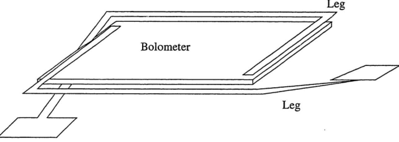
wave-lengths from 7-14 um. Each bolometer is thermally isolated from its surroundings by
a small bridge, supported by two thin legs. Each pixel is about 50 Aim x 50 jim in area and 0.5 m thick, yet microbolometers can typically withstand thousands of g's
of shock.
Despite improvements in microbolometer technology, sensors have not reached
theoretical performance levels. For a given set of optics, the ability to see an object clearly is limited by the sensitivity and noise of a device. Reducing system noise will
allow one to make out finer details and see smaller objects. The goal of this thesis was to measure the relative contribution of various noise sources and then determine
what can be done to help reduce the noise. Both detector and read-out integrated circuit (ROIC) noise are important and were considered, but bolometer noise was a larger focus of the study.
Chapter 2 is concerned with testing individual bolometers without the compli-cations of system noise. It begins with a brief review of bolometer terminology. Construction and verification of the test setup used in measuring bolometer noise is
then discussed.
Chapter 3 presents the results obtained from testing a large number of bolometers. Various models are fitted to the data in order to determine the cause of the noise.
Based on the results of testing, several new experiments were proposed to reduce noise. The results of one experiment are discussed.
Chapter 4 develops a basic framework for noise in the investigated Uncooled
sys-tem. Two basic figures of merit for evaluating system performance are presented. The results of the system model are compared with data on numerous focal planes to ensure its validity.
Chapter 5 details how various components of the system noise were separated from one another. The major sources of system noise are identified and quantified.
Chapter 2
Single Element Testing
2.1
Overview
One main reason for testing individual bolometers is to obtain measurements free
of the complications of system noise. If tests are only performed on a system level with all noise sources present; then it is often difficult to determine if the bolometer
noise component has been correctly isolated. Constructing a test station capable
of reporting the Johnson noise of resistors from 10 to 50 k (roughly the range of resistance found in actual bolometers) requires a very low-noise amplifier, mainly
because of the low frequencies involved. An ideal system would be able to measure Johnson noise to well below 0.1 Hz, but anything which performs well to about 1 Hz is adequate.
A general block diagram of the system used to achieve a low noise measurement is outlined in Figure 2-1. The test box is the most critical part of the testing. In an
actual system, the parts are biased to about 1 uWatt, so the test box must be able
to bias to this level. The test box also provides a gain of 1000 to bring the signal
to a measurable level and create relative immunity against noise sources entering
after its output. The two multimeters are used to record bias, measure bolometer resistance, and monitor output voltage for calibration of the test circuit. The Model 113 pre-amplifier serves mainly as a high-pass filter at the low end of the frequency
High Node
Bias Monitor
Test
Out
Figure 2-1: Test setup overview
the 113 amplifier can also be used for an additional gain of about 10 and low-pass
filtering. The HP dynamic signal analyzer measures the noise power spectral density for bolometer noise.
There are several benefits to single element testing. As mentioned before, the
interpretation of the results is relatively straightforward. In addition, single-element testing can be done at an early stage of device fabrication. If noisy parts are caught
early, then costly processing steps can be eliminated for bad parts. The rapid feedback possible with this measurement enables a wide variety of testing to be performed in a short period without worrying about system noise fluctuations.
Testing individual bolometers cannot completely substitute for system-level
test-ing. First, bolometers for testing are isolated so that metal contact probes can easily reach them. From photographs of parts, it is apparent that isolated bolometers
of-ten undergo a slightly different amount of etching than clustered pixel bolometers. Furthermore, test parts are located near the edge of an array, and only over a small region. If there is substantial variation across a wafer, then a few test parts may
mis-represent the focal plane. System-level testing, backed solidly by testing of individual bolometers seems to be the best solution.
2.2 Bolometer Overview
A bolometer is a resistor whose resistance is a function of its temperature. Semi-conductor bolometers usually drop in resistance as temperature rises, while metals exhibit the opposite behavior. By measuring the fractional change in resistance, one can measure a temperature change in the environment.
The bolometer technology investigated here was developed by Honeywell. A thin layer of vanadium oxide (VOx) is sandwiched between two thin insulating layers. VOz is a temperature-sensitive material, undergoing a larger fractional change in resistance for a given temperature change than many other semiconductors.
In order to achieve high thermal isolation, each bolometer is suspended above the substrate. Two small legs provide the only support for a bolometer (see Figure 2-2). Despite its precarious position, a bolometer is actually quite rugged because of the small scale.
Leg
Figure 2-2: Single bolometer
Several terms need to be defined before going into any analysis on bolometers. The thermal coefficient of resistance (TCR) is a measure of the percentage drop in resis-tance per degree change in bolometer temperature. The equation for a semiconductor is given as [10]:
1
R =
TCR=
RJ
--
(2.1)
where and Ro are constants dependent on a given semiconductor. Thermal capacity
(C) is a measure of how much heat a pixel holds. It is similar to electrical capacitance,
and is determined by device geometry and material. Thermal conductance (G) is a measure of how fast heat is transferred between a bolometer and its environment. For a given bolometer technology in a vacuum, G is mainly determined by heat transfer through the leg materials; radiative loss is negligible.
The response of a bolometer to a signal is given by [5]:
V
,= IAR = IR(TCR)
(2.2)
where I is the current through the device, R is the bolometer resistance, and P is the
power incident on the device.
Semiconductor bolometers with a negative TCR need to be tested with care; if one biases them too high, then an unstable condition causing burnout can be reached. As the resistance drops more current flows, leading to more Joule heating and a further drop in resistance. The cycle can continue until the device burns itself out.
Bolometer thermal characteristics determine the response time to a signal. , or the effective thermal time constant, is G. For the examined technology, r is usually on the order of 10 ms, which substantially limits detector response time. For this reason, the examined bolometers can only be used in slow refresh rate systems (on the order of 60 Hz).
There are three main types of noise in semiconductor bolometers: white noise,
flicker noise, and thermal noise. The white noise is Johnson noise, and appears in all resistors. Flicker noise has a 1/f noise spectrum and is usually linearly dependent on current. Thermal noise is caused by random heat exchange with the environment. The variance for each type of noise is given as [5]:
V2hite = 4kTRBWhite (2.3)
V/f = aVbiasBl/f (2.4)
thermal -
G
Vta4 s (TCR)2Bthermal (2.5)where k is Boltzmann's constant, T is the bolometer temperature, Bnoi,e are the noise effective bandwidths, a is an unknown proportionality constant, and Vbias is the bias on the bolometer. The thermal noise was never observed because of its low level (caused by a high G). Note that white noise can be easily separated from 1/f noise because of their different spectral characteristics.
When evaluating system performance, a better figure of merit to use is noise equivalent power (NEP). NEP derives directly from the voltage noise variance as
follows [5]:
G
NEP = TCR Vj (2.6)
where V is the noise voltage. Assuming TCR and G stay relatively constant for a given process, a good noise figure of merit is Vn/Vbias.
2.3 Test Station Equipment
A test box was designed and built to measure Johnson noise on bolometers down to 1 Hz. The basic design consists of an N-stage parallel bridge circuit. By choosing an appropriate number of stages, one can optimize the noise characteristics of the overall amplifier for a given bolometer resistance. Using standard low-noise op-amps, an 8-stage design meets the required testing specification. One must be able to measure the Johnson noise on a 10-50 kQ resistor to frequencies less than 1 Hz.
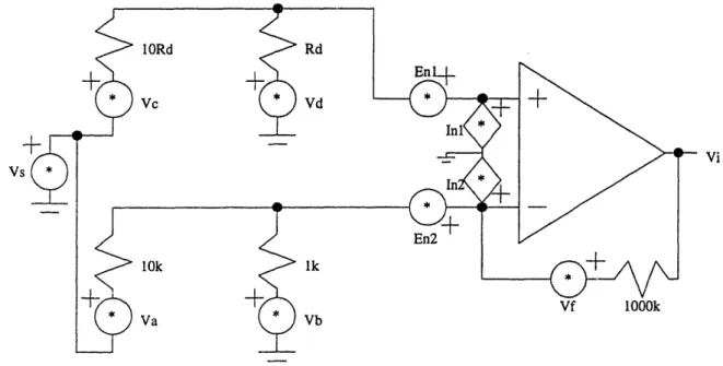
A diagram of 2 of N stages of the bridge circuit is shown below in Figure 2-3. Two inputs, "high" and "low," are connected to the bolometer, or device under test (DUT). Three outputs provide access to information which specify the operating parameters of the circuit. The "bias monitor" is the voltage across the top of the bridge, or approximately 11 times the voltage across the bolometer. The "hi monitor" is a direct measure of the bias across the bolometer. The "out" node is where the HP3561A makes its noise spectrum measurements. The DC level of the output gives feedback as to when the circuit is balanced. A low-noise voltage reference provides the bias voltage across the bridge. For the circuit to be balanced, the voltage across the DUT must equal the voltage across each 1 kQ resistor. Adjusting the 500 kQ
Vs
LM399
+9V
)Ut
1000k
Figure 2-3: Bridge circuit : 2 of N stages
potentiometer until the DC output is 0 volts balances the circuit.
Motchenbacher and Connelly [8] provide a differential amplifier noise model, en-abling one to estimate the performance of the noise circuit. The model for a single op-amp is shown below in Figure 2-4. Before drawing the equivalent noise model of
Figure 2-4: Differential noise model for an op-amp
the circuit, a small simplifying assumption will ease the analysis. The point labelled Vs in Figure 2-3 is approximately a voltage source with noise given by the voltage reference noise divided by the biasing potentiometer resistor ratio. For small changes in the DUT resistance the voltage at Vs will not change much, so the approximation holds.
Figure 2-5 below shows a noise equivalent model for one stage of the amplifier.
hi node"
For simplicity, each noisy resistor has been replaced with a voltage noise generator and a noiseless resistor. For N-stages of Figure 2-5, and without connecting the
lORd Vc En2 10k Va lk Vi Vb
Figure 2-5: Noise model of 1 stage circuit
op-amp outputs together, the voltage
i= 1, 2, ... , N):
at the output of each stage is given by (for
1101 11010 1
Vi = -10OV- OVb+ 11 vc+ 1---Vd+ s + Vf +
11010
1101 (E,
-
E
2)
+ N
RdInI
-1061,2
11 (2.7)
Connecting all the op-amp outputs together through 10 kQ resistors, and modeling
each op-amp as a voltage source gives the following output voltage variance:
(2.8)
1 N
Finding the total variance requires one to determine which terms are correlated for the final sum. The correlated terms include Vc, Vd, and V, since each op-amp sees the right half of the bridge in Figure 2-3 as the same. The current noise term involving
Inl is identical at each stage, so it does not average out. Uncorrelated terms include
Va, Vb, Vf, E,, and In2. The total variance at the output thus reduces to:
104 106- 2
Vt2otal
V + V + 104V2 + 106V2 + 106Vd + 1/121 V2 +1 1.12 10 1012
V
2+ 1.12
E2 +
N*
10
6RaIl +
,12
(2.9)
The voltage noise ternis are averaged out because they appear independently at the
output of each op-amp. The current noise (In1) of each op-amp increases the total current noise of the circuit because all the terms are perfectly correlated (i.e., all the
noise current flows through the DUT).
To achieve the necessary performance, parts were selected for their low-noise char-acteristics. Bypass capacitors installed on each voltage source reduced high-frequency
noise. The OP497 op-amp was used in place of the AD745, even though the AD745 has better noise characteristics. Unfortunately, the AD745 had an unreasonably long
delivery time, thus making the OP497 the only feasible choice. Chopper amplifiers also fell under consideration because of their low 1/f noise, but were rejected because of their high voltage noise. Too many stages would be required to reduce the voltage
noise to an acceptable level.
Metal film resistors were used because they exhibit significantly less 1/f noise than carbon-based resistors. Three 9-volt batteries power the bridge circuit in order
to avoid ground loops and 60 Hz power-line noise. One battery powers the LM399 voltage reference, and the two others provide the positive and negative polarity for
each op-amp. The entire circuit is surrounded by a metal case which is tied to ground; thus some EMI is blocked by the case. The performance of the LM399 is adequate
because its noise is not amplified at the output, as seen in Equation 2.9.
Carbon-based potentiometers, much like their resistor counterparts, are much too noisy for noise-sensitive applications. Two choices remain: cermet and wire-wound
potentiometers. Wire-wound potentiometers tend to have the lowest noise, but are difficult to find in high-resistance values (i.e., 500 kQ); therefore, Cermet
poten-tiometers provide a good starting point. Selecting the potentiometer also required some thought into ease of testing considerations. To keep the DC output voltage from
changing less than 1 volt when V -_ 4 volts, the percentage change in the potentiome-ter resistance must be less than about 0.3%. In the worst case, the potentiomepotentiome-ter
resistance is as low as 100 kQ, so adjusting to within 300 Q may be necessary. Placing two 10-turn 10 kQ potentiometers in series with the 500 kQ potentiometer allows one to adjust within 500 Q for half a turn, which is more than enough resolution.
2.4 Environmental Sources of Noise
Even if the electronic circuitry of a test station has negligible noise, one must be
careful to reduce environmental sources of noise. Changes in the environment can generate false signals which show up as noise. For a test station, repeatability of measurements is a major concern.
One potential source of noise is microphonics. Microphonics are small vibrations in the environment which can produce noise in electronic circuitry. A common source of microphonics is motors. For example, a vacuum pump motor operated across the room from the test station generated a significant amount of noise.
Eliminating the microphonics noise allows one to get a better estimate of bolome-ter noise. Placing the entire test setup on a granite block reduced vibrations
substan-tially. The granite block, with rubber padding beneath it, acts as a low-pass filter. A flexible padding beneath the test box itself further reduced vibrational noise.
Air currents flowing over a bolometer also posed a problem because they introduce a substantial amount of noise. Reduction of air currents was accomplished in a few ways. Enclosing the entire test setup in a box reduced air flow over the part; walking
near the test station no longer generated spurious noise signals. More strict tests
can be done to determine if environmental fluctuations are still a significant source of the measured noise. Placing the bolometers in a vacuum completely changes the
amount of contact they have with the environment. If the measured noise is
differ-ent on bolometers in vacuum and bolometers in air, then environmdiffer-ental fluctuations
are a likely suspect. Another simple test involves measuring the noise on
two thin legs (the standard configuration). If the noise changes dramatically, then environmental fluctuations are a potential cause.
Light also affects bolometer noise measurements. The measured resistance of an,
illuminated bolometer is different from the same bolometer in darkness. If a light source is not steady during measurement, then the resulting signal shows up as a substantial source of noise. For testing, the bolometers were kept in darkness.
Since a bolometer is thermally connected to its substrate, changes in substrate
temperature may show up as noise. One solution is to place the substrate on a large block of metal; the large thermal constant of the metal prevents rapid temperature
changes.
Electromagnetic interference (EMI) can also contribute to measured noise. Most commonly, radiated signals are picked up through loops of wire in the test setup.
Ground loops were mostly eliminated by using a battery powered test box, thus reducing EMI. Placing the entire test setup in a metal box also reduced EMI since
the box acts as a Faraday cage. Power line noise was not much of a problem, because the frequencies of interest were all below 40 Hz. The 60 Hz noise did not spill down into the 40 Hz range.
2.5 Filtering Out Unwanted Noise Sources
The spectrum analyzer computes an estimate of the power spectral density (PSD)
over the frequency range of 0.1 to 40 Hz. A few artifacts may appear if care is not taken to appropriately filter the signal before processing. In particular, both high and low frequency content need to be considered to eliminate false results.
The signal from the test box must pass through a low-pass filter before it is sampled to avoid aliasing. Fortunately the HP3561A spectrum analyzer handles the
anti-aliasing filter, so one does not need to worry about aliased noise.
Without a high-pass filter a low-frequency artifact shows up with a l/f 2 spectrum,
thus covering the bolometer 1/f noise at low frequencies. The artifact arises because
substrate may be changing temperature very slowly, or the bolometer may be heating
its surrounding environment. The 1/f2 spectrum is greatly reduced by filtering out
frequencies below 0.1 Hz.
Before sampling, filtering out frequencies below 0.1 Hz reduces PSD frequency
components up to 10 or 20 Hz. This strange situation arises because two different time scales are involved in the measurement. In the continuous-time domain of the
analog filter, the drift component of the signal is a ramp multiplied by a long "box."
The Fourier transform of a long box (and its derivative) is concentrated very close
to 0 frequency. Placing the drift through a high-pass filter with a cutoff of 0.03 Hz eliminates a significant part of the frequency components and thus most of the drift.
In the HP3561A, however, sampling only occurs for 10 s at a time when measuring
frequencies down to 0.1 Hz. The slow ramp, if not filtered out in the continuous-time domain, appears as a ramp over a very short period of time. The discrete-time Fourier
transform (DTFT) then becomes:
sin (w (M + 1) /2) (2.10
sin(w/2)
where M = 400 is the length of the sequence and k is the slope of the ramp. The
DTFT has a much wider frequency content because of its short observation time.
On a log-log plot of the PSD, the slope of the noise looks like 1/f 2. The numerator of Equation 2.10 can be thought of as a modulation function, with the denominator
acting as the envelope of the waveform. Ignoring the zero values caused by the numerator and remembering to square the function for the PSD, for w much less
than r the denominator has a slope approximately given by:
1 4
I ' 4 (2.11)
(sin(w/2))2 W2
Filtering out the slow ramp with an analog filter removes the unwanted 1/f2
be-havior in the PSD. Care must be taken to prevent the l/f 2 artifact from overwhelming
the real 1/f signal, so the signal was put through a high-pass with a cuton of 0.03
2.6 Data Fitting and Reduction
The data from the spectrum analyzer contains contributions from several unwanted
noise sources, including test equipment noise. By fitting the data to a model and subtracting out the test equipment noise, one obtains a reasonably accurate measure
of bolometer performance.
There are three main types of bolometer noise, all of which can be separately identified by their PSD characteristics: white Johnson noise, which has a flat PSD;
flicker or 1/f noise, which has a 1/f spectrum; and thermal noise, which has a spectrum like bandlimited white noise. As noted before, the unique spectral shape of
thermal noise was never observed, so it was not included in the model.
The test setup also contributes several types of noise to the measurement. Each
op-amp has some white noise and some 1/f noise. Drift noise, as discussed before, may not be entirely filtered out by the analog high-pass filter, so it should be taken into account. Its PSD is approximately a 1/f2 spectrum (ignoring the zero points).
The types of noise mentioned above suggest a PSD model of the form:
S= = a2 + b2/f + c2/f 2 (2.12)
where a2 is the white noise variance, b2 corresponds to the 1/f noise variance, and c2 belongs with the drift noise. For a positive bias on a bolometer, both a2 and b2 contain contributions from the bolometer and the test equipment. Separating the two components is discussed below.
The HP3661A spectrum analyzer provides a noisy estimate of the PSD. The data taken consisted of an averaged set of 16 periodograms, each with 400 frequency points,
using a non-overlapping rectangular window. Some simplifying approximations help make the data fitting more tractable. First, each point of the data has an
approx-imately Gaussian distribution. The actual distribution of each point is chi-squared, but it approaches the Gaussian distribution as more averages are performed. Also, the 400 points in each window of the periodogram are assumed to be relatively
a2, b2, and c2can be found using a non-random parameter estimate method. Based on the model in Equation 2.12, the vector of data points may be thought of as:
y=
Hy+
(2.13)
1 l/fi l/f 12 a2
H= , b2 (2.14)
1 l/fN 1lfi2 2
where f, is the nth frequency point, V is a column vector of measured data points,
and w is 0-mean Gaussian white noise with a covariance matrix A,.
In order to solve the equation, Aw must be known. For Gaussian noise and large
N, it can be shown that [7]:
K-i
f
2S2 (ew) w 2= , r
ar{ =X KS j = (2.15)
=K
=O
kS2
(e
i)
jotherwise
where K is the number of averages and Ir is the rth periodogram with N points. The variance of each periodogram point in A, is approximately V divided by the number of averages performed (except at w = 0, r ).
The probability density function (PDF) of V parameterized by x is given as:
py (; T) c e ( ~- H )T- a ~(~ H ) (2.16)
To find the maximum-likihood (ML) estimate of x, one must maximize py (V; x). The
resulting ML estimate is:
ML
=
(HTA-1'H) HT A` (2.17)The ML estimate is exactly the same as doing a weighted least-squares analysis of the
data (using a statistical weighting). A standard least-squares fit would give undue attention to the lower frequency points because of their high noise levels. A weighted
least-squares fit gives equal attention to all noise levels.
Two important figures of merit for any estimator are bias and error covariance. The expected value of -ML is , so it is an unbiased estimator. The covariance of
XML is:
A:= (HTA
1H')
(2.18)The variance of a2, b2, and c2appear directly on the diagonal of the covariance matrix, so finding an error bound is relatively straightforward.
It is sometimes more convenient to express results in terms of standard deviations (a) instead of variances (a2). To convert the error bound of &2 to an appropriate
bound on &, let f = x1/ 2 and find how a small change in x affects f:
dx 2v1 , thus Var
[1l
Var [x (2.19)The above approximation only works if the variance of x is much smaller than its mean value. Since 16 periodogram averages were performed, the variance should be a factor of 16 below the mean, so the approximation is valid.
Some numerical simulation showed that the fit to data is somewhat lower than expected. The main reason for the error is because points with low values are given lower variance and thus a heavier weight. A spurious low point can drag down a
measurement. By running the fitting algorithm more than once, one obtains a more accurate (i.e., less biased) fit to the data. The first iteration uses the data points over the number of averages as the variances. Each successive iteration uses the fitted curve of data points over the number of averages as the variances.
Once the noise data is fitted to a2 and b2, the test station noise should be separated
from the bolometer noise. The bolometer 1/f noise separates easily from the test station 1/f noise when one considers data at 0-bias and a positive bias across the bolometer. There is no measured bolometer 1/f noise at 0-bias since no current is flowing through the part; therefore, subtracting the 0-bias value of b2 from the its
corresponding positive-bias value yields the part of b2 from the bolometer alone. Isolating the bolometer white noise is complicated because both the test station
and bolometer white noise are independent of bias. The measured white noise variance in a unit bandwidth is given by:
a2
1.21 V,2
+ 16iR2 +4kTR
(2.20)where V2 is the op-amp voltage noise variance, and i2 is its current noise variance. By observing the c2 for various values of R, one may approximately find V2 and
i2. In addition, the OP491 data sheet provides a rough idea of what the two values should be.
2.7 Test Procedure
The test procedure followed is easy and yet provides all the essential quantities of
interest. In addition, it gives a way to identify problem measurements during testing and allows verification of data during analysis.
The resistance of a test bolometer is measured for a given bias voltage. The bias
voltage chosen is about 0.4 V (or about 0.04 V across the detector itself). The bias voltage is low enough so that heating of the bolometer is relatively negligible. After
setting the bias, the bridge is balanced so the DC output level is 0 V. The top half of the bridge resistance (Rc) is now 10 times the bolometer resistance. Rc is measured
by recording the voltage at the "bias monitor" node and then the current from the "hi
node" when it is connected to an ampmeter. The DUT resistance (Rd) is obtained
by taking the ratio of voltage to current.
Noise measurements occur at 3 bias points: 0, 1, and 1/4 /Watt. The 0 bias point gives the test box 1/f noise alone, along with a good measurement of the bolometer
white noise. The 1 uWatt bias point is representative of the bias power used in actual operation of the device. The 1/4 jpWatt bias point is useful because the applied
voltage is half of its value at the 1 pWatt point. If the measured 1/f noise looks
2.8 Excess Noise
To verify the test station, noise on several metal-film resistors was measured. As bias increased on the resistor, 1/f noise increased as well. The measured 1/f noise should remain constant over all bias values unless the DUT has 1/f noise. Since metal-film resistors have low 1/f noise, the test station generated the extra noise. Replacing a part in the test box fixed the problem.
The source of the extra noise was the 500 k Cermet potentiometer. Testing a
150 Q2 resistor allowed the bridge to be balanced using one of the two smaller 10 kQ potentiometers alone. No significant noise increase was observed from either small potentiometer. Testing a 21.5 k resistor and using the large potentiometer resulted
in a large increase in noise with increasing bias. Both burst noise and 1/f noise were present.
After a few other 500 kfl potentiometers showed similar noise problems, a switched
resistor network solved the problem. Six switches and resistors created a discrete potentiometer, with values between 0 and 480 kQ at 20 k intervals. The circuit is shown in Figure 2-6.
Figure 2-6: Switched resistor network
2.9 Test Pad Contact Noise
The test bolometers are not accessed in the same manner that bolometers in an array are. Test bolometers are wired directly to test pads on the side of a chip, while normal bolometers receive on-chip amplification before being measured. Test bolometers, because they receive no on-chip boost, are more sensitive to test pad
-contact noise. Even if the test pad -contacts are noisy, it is of no interest for the
actual operation of the device.
A few different approaches were taken to verify that the measured 1/f nnise was not due to contacts. First, data on normal metal-film resistors should show if there is
a problem with the test station contacts themselves. Next, 1/f noise in the test pad contacts is a larger problem for low bolometer resistances. The noise figure of merit is V,/V, which is proportional to R/R. An R, term caused by the test pad contacts
should be relatively independent of the bolometer resistance. For a given R, lower
bolometer R increases the the noise figure of merit V,/V if the problem is contact noise. A plot of the noise figure of merit vs. resistance is given in the following results
section. In addition, the test pads were bonded with metal to another completely different kind of contact. The tests were then repeated under similar conditions for
the same bolometers. If test pad contact noise were a problem, then some difference in the measured noise should be visible.
2.10 Results
2.10.1 Resistance Measurement
The resistance measured by the test box approximately corresponds with the
resis-tance measured by an ohmmeter. Table 2.1 below gives a couple standard comparison measurements between an ohmmeter and the test station.
Ohmmeter R(kQ ) Test Box R Ratio
10.2 10.0 0.98
21.5 20.4 0.95
Table 2.1: Resistance verification
The accuracy of the test box has about a ±5% error. One reason for its
inaccu-racy is that voltage and current across the resistor are not measured simultaneously; loading of the test box by the current meter changes the operating point slightly.
2.10.2 Drift, Reduction
Passing data through a high-pass filter reduces the drift component of noise substan-tially. Several parts have data both before and after the benefit of filtering. Table 2.2
below shows data for several representative parts, where "c" is the constant fitted to the 1lf2 noise component (see Equation 2.12).
Table 2.2: Drift reduction
Drift noise initially is comparable with the 1/f noise at low frequencies, and thus it clouds a visual assessment of the noise. Reducing the drift noise component by a factor of 2-3 makes the noise look more 1/f and improves the 1/f fitting routine.
2.10.3 Validating the White Noise
Verifying that the white noise measured by the station is approximately correct helps
validate the data collection process. Extracting the white noise of a bolometer requires a knowledge of the voltage noise of the op-amps. According to the OP491 specification
sheet, current noise should only provide a 1/f component at low frequencies. Equation 2.20 shows the major components of white noise in the system.
Two methods were used to compute the white noise of the test box. First, measuring the noise on a known low-resistance Lietal-film resistor gives the
volt-age noise almost exactly. In this case, the measured white noise on a 150 Q resistor was a total of 6.4 nV/v/IHz. The actual white noise on the resistor is theoretically
/4kTR 1.6 nVv/H, thus the total voltage noise is about 6.2 nV/v/HIz. According
to Equation 2.20, the variance on each op-amp is 16 times greater, so the noise per Part ID Type "c" 107, no filter "c".107, with filter
20.08.04 F2 1.26 0.60 F3 0.98 0.28 20.11.10 F2 1.23 0.28 F3 1.07 0.23 20.11.05 F2 2.36 1.03 F3 0.50 0.18
root hertz is 4 times greater, or approximately 25 nV/v/-.
To further verify the voltage noise measurement, white noise data on 100 parts was compared with the theoretical white noise value for each part. On average, the extra white noise was about 6.2 nV/vHzi; therefore, the two results agree very well. The
OP491 data sheet confirms that the estimated voltage noise is reasonable. The data sheet specifies a typical voltage noise of 17 nV/Viz and a maximum of 30 nV/Hz.
The measured 25 nV/VHz lies comfortably in the data sheet range.
Figure 2-7 shows the distribution of ratios between the measured white noise (mi-nus the test box voltage noise) and the theoretical white noise. The actual standard
2
cl
C
.0
E
Ratio of measured to theoretical white noise
15
Figure 2-7: Histogram of measured / theoretical white noise
deviation on the measurements is about 4%, even though the predicted standard
de-viation is only about 1%. The measured resistance used for the theoretical white
noise value is only good to within ±5%, and so it introduces more uncertainty.
A,
2.10.4 Repeatability
One important aspect of any test is the ability to repeat results. The repeatability
measurements done carry the idea even farther, as the parts were tested under two completely different environmental conditions. Bolometer response is very sensitive
to the thermal conductance with its surroundings, thus testing the parts in air and in vacuum is a solid test to see if environmental fluctuations matter. In order to test parts under vacuum, the bolometer test pads had to be wire-bonded to a chip. As discussed before, if test pad contact noise were a problem then some difference should be observable in the measured noise.
The three conditions tested were: "Standard", "New Contacts", and "Vacuum." The "Standard" configuration means that the bolometers were tested in air with the normal test pad contacts. The "New Contacts" configuration was after the bolometer test pads had been wire-bonded to a chip, but the test was still performed in air. The
"Vacuum" configuration occurred when the "New Contacts" parts were placed under a vacuum.
The graph in Figure 2-8 shows a normalized noise figure of merit (Vn/V) for each wafer tested. There are several parts on each wafer. For each part, the mean of
Vn/V was taken across all measurements in different conditions. The Vn/V for each
test was then divided by the mean. In an ideal case with perfect measurements, the resulting normalized noise figure of merit would be 1 for all the data points. With
uncertain measurements, however, there will be some spread around 1. The vertical
line in the graph is 3 standard deviations of the maximum predicted error (ignoring
error in the calculated mean), so basically all of the data points should fall on the line. A small part of the data from the "Standard" configuration is more variable because it was not tested inside a box. When people walked by, the noise would increase a
little bit, thus giving a few scattered high points on the graph which do not lie within the predicted error. A single high point is enough to disturb the calculated mean and
cause a few points to fall below the error bound as well.
ba-sically the same. The unchanged results given a large change in the environment strongly suggest that environmental fluctuations do not contribute significantly to
the measured 1/f noise.
0 0 I x I I I l I I II 2 4 6 8 10 Wafer number W X A.,/ x In Vacuum o New Contacts K Standard , , 5 Ii I vE :( II X x -i I X 12 14 16 i8
Figure 2-8: Repeatability test
2.10.5 Excess Test Box 1/f Noise
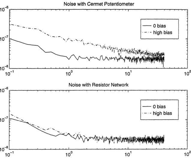
The 1/f noise of the test box alone should not change with bias. By testing a metal
film resistor with low 1/f noise, one can see if any resistors in the test box exhibit 1/f noise. The first round of tests showed that 1/f noise increased strongly with bias (see Figure 2-9). Replacing the 500 kQ potentiometer with the resistor network described in Section 2.8 virtually eliminated the problem; 1/f noise becomes independent of bias (see Figure 2-9).
1 .5 1.2 2 1.15C o 1.1 t- 1.1 > 1.05 0 co E 1 >0.95 0.9 n n A
.1
II 0v.v 0 I, I I I I I I I I i W II I i I I I I 11 I I I INoise with Cermet Potentiometer
100 101
Noise with Resistor Network
100 101
Figure 2-9: Test box 1/f noise and bias
2.10.6 1lf Dependence on Current
1/f noise typically scales linearly with current. Since all parts were tested at two
biases (plus a 0-bias), it was easy to verify that the measured 1/f noise did in fact
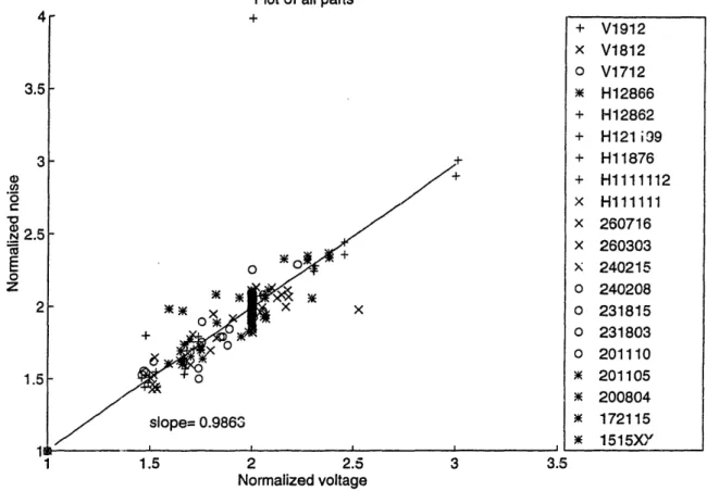
scale linearly with applied voltage (and thus current). Figure 2-10 shows a normalized noise plotted versus a normalized bias voltage. For each part, the two measurements were normalized to the noise and bias level of the lowest measurement.
I I I I I I I
.
|--. Obias
.-.- - high bias ..~~~~~~~~~~~~~~~~~~~~~~~~~~~~ 10- 6 10-7 10- 8 1C 10-6 10- 7 10 icI
1( ," ' . I , ' I ' ' ' I ' I ' '' ' i *1 - 0 bias - - high bias i " " ' . .. I ·. I 1(I
i I , 1 I 1 I 1 I I I i I I i. i I I 1 I I i _ )-1 )-1 )2 )2Plot of all parts -I + 0 T * + x + slope= 0.9863 1.5 2 2.5 3 Normalized voltage + V1912 x V1812 o V1712 3 H12866 + H12862 + H121 i99 + H11876 + H1111112 x H111111 x 260716 x 260303 x 240215 o 240208 0 231815 o 231803 o 201110 3 201105 X 200804 W 172115 * 1515XY 3.5
Figure 2-10: Linear dependence of 1/f noise on current
2.10.7 Contact Noise
Test pad/test probe contact noise does not affect the measurements taken. As seen in Figure 2-9, normal resistors showed no excess 1/f noise; therefore, they had no test probe contact noise. In addition, lower resistance parts should be more affected by contact noise. Figure 2-11 shows that AR/R actually decreases as R decreases, thus test pad contact noise is not present. Further evidence that contact noise is not
a measurable source of noise is presented later.
4 3.5 3 2.5 0 C -o a 0
z
2 1.5 1 lrx 10- 6 + K + x I mm X lx l c l
0.60.
1
12
.41.
0.6 0.8 1 1.2 1.4 1.6 Resistance (ohms) x104Figure 2-11: Contact noise test 1.4 1.3 1.2 1.1 1 0.9 0.8 0.7 0.6
Chapter 3
Bolometer Tests
3.1
Overview
Verification of the test procedure paves the way for extensive testing on parts in hopes of finding the cause of 1/f noise. The magnitude of the 1/f noise can be put into system models where its relative importance can be determined. The main goal of testing is to find how much 1/f noise affects system performance, and how to reduce
its impact.
There are several advantages to single element testing over system testing. Parts that do not work in an actual system can still be characterized by a robust test station. The wider range of experiments possible gives more information on determining how to reduce 1/f noise. Also, the rapid feedback possible allows more data to be collected without spending time and money on building entire systems. Analysis of single element testing is much simpler than analyzing an entire system.
The main strategy consisted of testing a large number of parts fabricated over an extended period of time. If any change is visible, then it may be correlated back to a change in a processing parameter. The main process changes observed include variations in pixel geometry, resistance, thickness, and stress. Except for thickness, most process variations are present on every wafer manufactured.
3.2 Background on 1/f Noise
Flicker noise, or 1lf noise, has been observed in a wide range of systems, from
the height of the Nile river over the last century to semiconductors. Despite its
ubiquitous presence, there is no unified theory for its source in semiconductors. Its main characteristic is a 1lf power density spectrum (PSD) down to any measurable frequency. 1lf noise is usually observed as a voltage or current fluctuation. Clarke and Voss [9], however, showed that it is really a resistance fluctuation that causes 1/f noise.
Hooge's empirical model characterizes a wide range of noise in metal films with only a single fitting constant. The formula for the normalized resistance PSD is given
by [ll]:
SR(f) a
SRUf) _ a (3.1)
R
2Nf
where SR(f) is the resistance PSD, R is the resistance, a 2 10-3 is a fitting parameter, and N is the number of carriers in the sample. Although Hooge's model works well for metal films, it doesn't always work for other materials. Hooge's formula
is commonly thought of as a volume effect, since N is proportional to the volume of the resistor.
Another important set of experiments on 1/f noise came from Clarke and Voss.
They hypothesized that 1/f noise may arise from spontaneous temperature fluctua-tions in a material. The temperature fluctuation model has an interesting consequence
for bolometers, since a higher TCR (temperature coefficient of resistance) will lead to more noise as shown below:
R
where -~ at 1 Hz is equivalent to the noise figure of merit. The above equation is a direct result from the definition of TCR (see Equation 2.1). As evidence for their model, Clarke and Voss observed that manganin, which has a TCR of virtually 0, has
goes down as volume increases.
3.3 Tested Parts
Standard test bolometers are fabricated on the side of every wafer to allow resistance,
TCR, and other basic parameter measurements. Testing standard parts has the
advantage of being able to examine parts ranging over a wide period of time. With a large amount of data, correlations between processing parameters and noise are more likely to show up. Unfortunately, the test bolometers were not designed with noise measurements in mind; therefore, sometimes different test pixels do not give significantly different information.
For the test pixels, a few basic parameters were varied. The parameters include geometry, contact area, and isolation/stress. None of the pixels are rectangular, but for simplicity their shape can be approximated with a rectangle having some effective width and length. Before etching, pixels are connected directly to the substrate. After etching, pixels are suspended above he substrate by two thin legs. On each wafer, pixels connected to the substrate and suspended pixels are present. For standard testing, the 6 types of pixels are: F2, F3, F2L, F3L, F5, and F6. The differences in important parameters for each pixel type are given in Table 3.1.
Table 3.1: List of part types
A "yes" to "suspended?" means the pixels have been etched away from the sub-strate, R is the approximate resistance, I is shortest distance between the two contacts,
and Wcontact is the width of the contacts (or size along the bolometer width). The Pixel I (shortest) contact Suspended? R
F2 15 38 yes 1.4 F3 15 38 no 1 F2L 27 19 yes 4 F3L 27 19 no 2.7 F5 14 22 yes 1.5 F6 14 22 no 1.1
resistances given are relative to the smallest value.
One important feature of Table 3.1 is that the resistance for parts with the same geometry (e.g., F2 and F3) is not constant. To suspend parts above the substrate, a layer of material is etched out. After etching, the resistivity of a part changes.
There are a number of difficulties with Table 3.1. First, the effective width and length of any pixel is not known. The values in the table give a length and width which should be roughly proportional to the actual size of the device. Also, pixels have corners, meaning that the current flow through them is not uniform. For simplicity, all models assume that the current flowing through a device is uniform. Next, the two contacts do not have a constant distance between them. It is often difficult to find the exact fraction of the contact area that has a significant amount of current flowing through it relative to the rest of the contact. From pixel design to pixel design multiple things change at the same time, thus clouding analysis. In future tests, only one variable should be changed between pixels. Designing a simple geometry (i.e., rectangular) would further clarify test results.
Two new pixel types were also tested. Fortunately the new pixels have varying thicknesses, an ideal test for differentiating between noise models. The two new pixels are L1 and L2. The L1 pixel is the same as the F2L pixel and serves as a control in the experiment. The L2 pixel is somewhat smaller than the L1 pixel. The approximate properties of each pixel are summarized in Table 3.2 below. The three wafers, V1712, V1812, and V1912, have VOx thicknesses of about 1000, 500, and 250 Angstroms, respectively.
Pixel Name I (shortest) Wcontact Suspended? R
F1 27 19 yes 4
F2 13 12 yes 2.8
3.4 Simple Noise Models
A few models of 1/f noise are needed to gain a straightforward understanding of the behavior of 1/f noise under different assumptions. The goal of such models is to help analyze data and find out where the noise is coming from. In addition, having
a simple model allows one to envision many different process variations which will distinguish between different types of noise.
One likely model for 1/f noise is a bulk effect, where the noise is generated
uniformly throughout the resistor. For a bulk effect, the noise can vary as:
NF = -n oc (3.3)
Vbias
V
where Vn = Sv(f = 1), Vbias is the voltage across the resistor, and V is the volume
of the sample.
The two basic quantities returned from each measurement are the noise figure
of merit (NF) and resistance (R). The NF is related to the resistance through two equations. The resistance of a bolometer is:
R=pt
wt
(3.4)
where p is the resistivity, and 1, w, t are the length, width, and thickness of the device,
respectively. Combining Equation 3.3 with Equation 3.4 results in the following
relation:
NF °c I = a (3.5)
Unfortunately, Equation 3.5 depends on the length of the bolometer 1. When testing various geometries, it is nice to normalize out the effect of having different lengths so
that intrinsic material quality can be compared. Using Table 3.1, one can multiply
NF/VR by its approximate length to get rid of the dependence on 1.
Another way to view noise is with a simple circuit model. Often, a simple resistor-based model is much clearer than a formula. For example, one can find the effect of
doubling the thickness of a resistor. Let the initial noise figure of merit be V V -- I=
a. Doubling the thickness of a sample is equivalent to having two resistors connected
in parallel, each with the same noise and resistance. The variance of the noise current through each resistor adds, so the new noise figure of merit is k As before,
i -sbe7 the noise goes down as the square-root of the thickness.
Another model for noise is a surface layer picture. The material near the surface of a bolometer undergoes a more rigorous treatment than the bulk, so it may be
more noisy because of damage. Bolometers are especially sensitive to surface effects because they are typically extremely thin (on the order of a few hundred Angstroms
thick). The circuit model for a surface layer effect is two resistors in parallel. One resistance is due to the surface layer and generates noise, while the other resistance
is the bulk resistance with no noise.
Assuming the bulk and surface resistivity are the same, the noise figure of merit works out to be:
NF oc 1 (3.6)
where w is the width of the bulk and surface, is the length of both sections, tb is the bulk layer thickness, and t is the surface layer thickness. Using the above equation, the following relation between the noise figure of merit and R arises:
NF
°loc-vR
(3.7)
Again, thickness is fixed, so the length can be normalized out in the same fashion
using Table 3.1.
Several observations need to be made about the above equations. First, for a fixed
thickness, there is no way to distinguish between a surface layer and a bulk effect by varying width and length alone (and given only NF and R). Next, the surface layer
model (Equation 3.6) predicts that noise will go down as v/7 when t, >> tb, and noise
will go down as tb if tb > t. The ratio of the bulk thickness to the surface thickness
determines how fast the noise drops as the thickness of a sample increases. Again, for simplicity the model assumes that the resistivity of the surface and bulk are the
same, even though it may not be true in an actual bolometer.
Contacts are an observable source of noise in many devices, so another potential model involves contacts. As previously described, the test pad contacts were ruled
out, but the contacts on the actual bolometer were not discussed. The circuit model
based on contacts is two resistors in series, with the contact resistance given by RC and the bulk resistance given by Rb. For simplicity, the two contact resistances are lumped together into one resistor. The bulk of the bolometer is assumed to contribute
a negligible source of noise.
The approximate NF, given that the measured contact resistance is much lower than any bolometer resistance, is given by:
1 R,
NF oc (3.8)
+/Aretact Rb
Note that as the bolometer resistance drops, contact noise becomes a larger problem.
It is approximately true for all the measured devices that the contact width is the
same as the bolometer width. With this assumption, the following relation arises:
1 (3/2)
NF oc - R (3.9)
For the contact model, a plot of NF normalized by R is more appropriate than a plot normalized by /-R As the width of the device goes up, NF/R should drop. Since all the contact lengths are the same, one can use Table 3.1 to normalize out the width
of the device (by multiplying by W3/2).
For all the above models, resistivity does not affect the noise figure of merit. If one
assumes that the noise varies with the carrier concentration (N) as 1/v/N instead
of with the volume as /v/V, however, resistivity plays an important role in noise
measurements. The noise figure of merit is now given as NF oc p/(w.t). Solving for the new dependence of NF on R and assuming a bulk effect model gives:
NF oc 1 (3.10)
If the noise figure of merit is a function of resistivity, then all the p terms disappear
when NF is divided by vA. Since resistivity changes when parts are etched, it is possible to distinguish between the volume and carrier concentration models.
3.5 Estimating Geometry with Noise
One extra application of noise measurements is that they allow one to estimate the length and width of a bolometer's electrically active area. If the model for noise is
known, then the results are relatively straightforward to interpret. If the approximate length and width of a pixel are known, then the estimation based on different models serves as a validation check for each model. If one has a simple pixel, then its length
and width are easily compared to more complicated geometries; thus, one can get a better estimate of the properties of complicated geometries.
The three basic models for noise are developed in Section 3.4. For a bulk noise effect, Equations 3.3 and 3.4 lead to a set of equations for length and width as given
below:
1 p
1c- and wC (3.11)
N( F NFV (3.11)
The exact relation between I and the two measured quantities R and NF may be found,
but it is often more useful just to compare how the length and width change from a standard simple geometry. If one pixel is rectangular and another has a complicated shape, then taking the ratio between the lengths of the two pixels gives an effective
length for the complicated geometry. Note that the width equation depends on p and t while the length equation does not; therefore, the width should only be compared
between pixels having the same resistivity and thickness.
Similar equations may be found from the various other noise models. For com-pleteness, the length and width equations are given below in Table 3.3.
Several features of the above models are worth noting. First, it is not possible
to distinguish between the bulk and surface layer model from length and width esti-mates alone. By varying thickness, however, the difference becomes apparent. The