Chalcogenide Glass Materials for Integrated Infrared Photonics
byVivek Singh
B.S. Materials Science and Engineering Columbia University, 2009
Submitted to the Department of Materials Science and Engineering in Partial Fulfillment of the Requirements for the Degree of
DOCTOR OF PHILOSOPHY at the
MASSACHUSETTS INSTITUTE OF TECHNOLOGY September 2015
© 2015 Massachusetts Institute of Technology. All rights reserved.
Signature of Author:_________________________________________ Department of Materials Science and Engineering July 20, 2015
Certified by:_____________________________________________ Lionel C. Kimerling Thomas Lord Professor of Materials Science and Engineering Thesis Supervisor
Certified by:_____________________________________________ Anuradha M. Agarwal Principal Research Scientist, Materials Processing Center Thesis Supervisor
Accepted by:_____________________________________________ Donald Sadoway Chair, Departmental Committee on Graduate Students
Chalcogenide Glass Materials for Integrated Infrared Photonics
byVivek Singh
Submitted to the Department of Materials Science and Engineering on July 20, 2015 in Partial Fulfillment of the Requirements for the Degree of Doctor of Philosophy in
Materials Science and Engineering
Abstract
Chalcogenide glasses (ChGs) are amorphous compounds containing the chalcogen elements (S, Se, Te) and exhibit wide infrared transparency windows. They are easy to synthesize in bulk and thin film forms and their compositional flexibility allows tuning of optical properties such as refractive index making them ideal for infrared photonics. We have studied the material attenuation in ChGs that arises due to the presence of impurities in the raw materials and established UV photolithography-based process flows that enable fabrication of chalcogenide glass waveguides and microresonators for near- and mid-IR wavelength ranges.
Waveguides and optical resonators are key microphotonic elements for many on-chip applications such as telecommunications and chemical sensing. In this thesis, we show that scattering losses dominate in our ChG microphotonic devices while material attenuation from impurities is low. We demonstrate resonators coated with nanoporous polymers to improve their selectivity against target analytes for sensing applications. We exploit the photosensitivity of As2S3 glass to build silicon-based tunable photonic devices that offer
post-fabrication tuning to optimize performance. Resonators also serve as a test platform for studying the effects of radiation on silicon and chalcogenide materials systems.
Further, we propose new mid-IR microphotonic device designs using ChG materials and the challenges associated with measuring mid-IR devices along with solutions to address them. We employ input-to-output offsets, standard tapered waveguides, and a fiber collimator to improve mid-IR measurements and demonstrate transparent ChG waveguides with losses as low as 2.5 dB/cm.
Finally, we propose a novel design that integrates PbTe detectors with ChG waveguides for on-chip mid-IR detection. Our simulations show that the use of a low-index spacer layer leads to a well-distributed field along the width of the detector due to a reduction in the effective index of the structure. We develop a fabrication process for waveguide-integrated detector designs and fabricate prototype structures that exhibit attenuation at telecom and mid-IR wavelengths. Such an integrated sensor design will enable the creation and deployment of low-cost remote sensor arrays with small footprints, and ultimately lead to “lab-on-a-chip” structures.
Thesis Supervisors:
Lionel C. Kimerling
Title: Thomas Lord Professor of Materials Science and Engineering Anuradha M. Agarwal
Acknowledgements
I distinctly remember the day in January 2009 when I received an email saying that I had been accepted to MIT and it took a few minutes for the news to sink in. Growing up in India, I had heard many great things about MIT but I never imagined that I would one day graduate with a degree from MIT. It has been a long journey and I want to recognize all those who had a hand in helping me get to this point.
I wish to start by thanking my parents. It could not have been easy for them to let their only child jet off to a foreign land on his own but they have always supported me with everything. I would not be here if it were not for their love and encouragement over the years.
My thesis advisors, Prof. Lionel C. Kimerling (“Kim”) and Dr. Anu Agarwal, welcomed me into the electronic materials research group (“EMAT”) during my first semester and I will forever be grateful for it. I could always count on Kim to provide meaningful solutions to problems that I ran into during my thesis work and lead me down paths I would not have conceived of on my own. His intuitive understanding of photonics and materials science is inspiring and he can always break down a problem into simpler parts to help me focus better. Anu has been my day-to-day advisor in EMAT since I started and this thesis would not exist without all her support and guidance through the years. She is always approachable and easy to talk to which led to many long conversations about not just my research but other topics as well.
The EMAT mentor list would be incomplete if I did not include Dr. Jurgen Michel. Although I did not get a chance to work with him directly until the last few months of my
research, I always appreciated his honesty, practical advice, and humor during group meeting presentations.
I would also like to thank my committee members, Prof. Silvija Gradecak and Prof. Caroline Ross for their helpful suggestions and direction during committee meetings and the preparation of this thesis.
Prof. Juejun “JJ” Hu, was my post-doctoral mentor when I joined EMAT and he has taught me much about photonics and chalcogenide glasses since then. Even after he left EMAT to teach at the University of Delaware, he was always available for discussions regarding my work over email and phone. His suggestions over the years and experimental assistance from his group members have been vital in the completion of this thesis work.
I have been extremely fortunate to collaborate with a number of brilliant scientists and engineers during the course of my Ph.D. Prof. Kathleen Richardson (University of Central Florida), Prof. Igor Luzinov (Clemson University) and Dr. Joel Hensley (Physical Sciences, Inc.) have been a part of our chalcogenide glass team since the beginning of my time here and it has been wonderful working with their respective research groups. Many of the important achievements in this thesis would not have been possible without their direction. EMAT has also played host to visiting scholars and I had the pleasure of working with Dr. Stefano Grillanda and Dr. Davide Bianchi from Politecnico di Milano on various projects.
I want to thank the staff at MIT’s shared facilities (MTL/CMSE) for training me on a number of instruments and for being patient with my questions. In particular, Paul Tierney and Kurt Broderick at MTL provided wonderful guidance when I was trying to design new process flows and were always available to answer my questions. Dr. Charlie Settens’ assistance at the CMSE XRD Lab was also very important. I wish to express my gratitude to Dr. Piotr Becla for helping with PbTe thin film measurements and Dr. Nilanjan
Chatterjee in the Department of Earth, Atmospheric & Planetary Sciences for his help with WDS data collection for my thin films.
I want to thank Kim’s assistant, Ms. Lisa Sinclair, for all her help with scheduling meetings with Kim, administrative concerns, and most importantly, her delicious cakes! She keeps the group functioning smoothly and EMAT is lucky to have her onboard. I extend my sincere thanks to Ms. Angelita Mireles and Ms. Elissa Haverty at the DMSE administrative office as well as the staff at the International Students Office for their assistance during my time.
Many former and current members of EMAT have formed an important part of my time at MIT: Dr. Timothy Zens, Neil Patel, Zhaohong Han, Brian Albert, Dr. Vivek Raghunathan, Dr. Michiel Vanhoutte, Dr. Yan Cai, Dr. Jianfei Wang, Dr. Jing Cheng, Dr. Rodolfo Camacho-Aguilera, Corentin Monmeyran, Brian Pearson, Dr. Kevin McComber, Dr. Xing Sheng, Dr. Kazumi Wada, Wei Yu, Dr. Lirong Zheng-Broderick, Dr. Jonathan Bessette, Dr. Jifeng Liu, Louisa Chiao, Dr. Pao Tai Lin, Dr. Lin Zhang, Dr. Clara Dimas, and Dr. Jianwei Mu. I had the pleasure of working directly with many of them on collaborative research projects within EMAT and I enjoyed the lively discussions we had on a variety of subjects. I want to extend a special thank you to Neil, Corentin, and Yan for helping me prepare for my oral exam.
I am grateful to Prof. Joshua Grossman (now at University of Maryland) and Prof. James Im (Columbia), my undergraduate advisors, for giving me opportunities to conduct research in their labs and learn valuable skills that have helped me during my time at MIT.
Finally, I wish to thank the rest of my family back in India for their love and support through the years. My friends, both at MIT and outside of it, played an important role in keeping me sane through these years by helping me take my mind off work
I dedicate this thesis to my maternal grandmother and a dear friend who unfortunately passed away during the course of my Ph.D.
Table of Contents
Abstract ... 3
Acknowledgements ... 5
Chapter 1: Introduction & Motivation ... 13
1.1 Chip-scale photonics ... 13 1.2 Infrared spectroscopy ... 14 1.3 Planar sensors ... 15 1.4 Mid-infrared materials ... 16 1.5 Mid-infrared detectors ... 19 1.6 Lab-on-a-chip ... 20 1.7 Summary... 21
Chapter 2: Chalcogenide Glass Materials ... 23
2.1 Infrared Transparency ... 23
2.2 Chalcogenide Glasses ... 24
2.3 Optical Properties of ChGs ... 25
2.4 Loss mechanisms in ChGs ... 27
2.5 Chalcogenide glass processing ... 31
2.5.1 Bulk glass synthesis ... 31
2.5.2 Thin film processing and characterization ... 31
2.6 Effects of radiation on ChG materials ... 35
2.6.1 Position annihilation lifetime spectroscopy ... 38
2.7 Other mid-IR transparent materials ... 41
2.8 Summary... 42
Chapter 3: Waveguides and Resonators ... 43
3.1 Dielectric waveguides ... 43
3.2 Dielectric microresonators ... 46
3.4 Mid-IR device design ... 51
3.5 Microresonators as a platform for studying materials behavior ... 54
3.6 Summary... 55
Chapter 4: Fabrication of Waveguides and Resonators ... 57
4.1 Photolithography ... 57
4.1.1 Projection lithography ... 58
4.1.2 Contact lithography ... 58
4.2 Thin film deposition ... 59
4.3 Lift-off process for ChG device fabrication ... 60
4.4 Process development for thick ChG waveguides ... 63
4.5 Other fabrication approaches ... 65
4.5.1 Electron beam lithography ... 65
4.5.2 Reactive-ion Etching of ChG materials ... 66
4.6 Summary... 67
Chapter 5: Near-Infrared Device Characterization ... 69
5.1 Near-IR measurement setup and procedures ... 69
5.2 Separating loss mechanisms in chalcogenide glass resonators ... 72
5.2.1 Experiment design ... 74
5.2.2 Separating material attenuation from scattering loss ... 75
5.3 Sensing experiments with polymer-functionalized resonators ... 76
5.3.1 Sensor functionalization using polymer coatings ... 76
5.3.2 Polymer thin-film-coated resonators ... 80
5.3.3 Polymer nanofoam-coated resonators ... 81
5.4 Exploiting photosensitivity to alter photonic device response... 84
5.4.1 Post-fabrication trimming of silicon-on-insulator resonators161 ... 84
5.4.2 Phototrimming of athermal amorphous silicon devices ... 87
5.5 Studying the effects of radiation on photonic materials with resonators ... 90
5.5.2 Chalcogenide glass resonators ... 95
5.6 Summary... 96
Chapter 6: Mid-Infrared Device Characterization ... 99
6.1 Mid-IR measurement setup and procedures ... 99
6.2 Demonstration of mid-IR transparent ChG waveguides ... 101
6.2.1 Design solutions to meet mid-IR challenges ... 101
6.2.2 Coupling to mid-IR sources ... 103
6.3 Chemical sensing with uncoated ChG devices ... 108
6.4 Silicon-based mid-IR waveguide systems ... 112
6.5 Summary... 116
Chapter 7: Lead Telluride for On-chip Photodetection ... 119
7.1 Infrared detection ... 119
7.2 Materials systems for IR detection ... 120
7.3 Characterization of PbTe thin films ... 122
7.4 Oxygen sensitization of PbTe ... 127
7.5 Optimization of key parameters for high signal-to-noise ratio ... 128
7.6 Waveguide-integrated PbTe detector design and simulations ... 130
7.6.1 Design overview ... 130
7.6.2 Electromagnetic simulations ... 131
7.6.3 Spacer layer materials ... 135
7.7 Integrated detector fabrication development ... 137
7.8 Testing waveguide-integrated PbTe detector prototypes ... 140
7.9 Summary... 142
Chapter 8: Summary and Future Directions ... 145
8.1 Chalcogenide glass materials for infrared applications ... 145
8.2 Infrared microphotonic device fabrication ... 146
8.3 Resonators as a platform for chemical sensing and more ... 146
8.5 PbTe for low-cost monolithic detector integration ... 147
8.6 Future directions ... 148
8.6.1 Resonator arrays with gradient nanofoams for sensing ... 148
8.6.2 Chalcogenide-on-sapphire as a mid-IR platform ... 148
8.6.3 Chalcogenide glass devices with undercut oxide ... 150
8.6.4 Development of an integrated light source ... 152
8.6.5 Chalcogenide glasses for nonlinear photonics ... 156
8.6.6 Electrical PbTe measurements ... 157
8.6.7 Electrical/capacitive sensing measurement ... 158
Appendix A: Impurities in Chalcogenide Glasses ... 161
A.1 Sources of impurities ... 161
A.2 Purification techniques ... 162
A.2.1 Chemical gettering and distillation ... 162
A.3 Impurity measurement with SIMS ... 162
Appendix B: Electromagnetic simulation tools ... 165
B.1 Film-mode matching (FMM) in FIMMWAVE ... 165
B.2 3-D FDTD with Lumerical ... 167
Appendix C: Loss separation calculations ... 171
Appendix D: The Importance of a Long Optical Path Length ... 175
D.1 Waveguides versus resonators for sensing applications ... 175
Chapter 1: Introduction & Motivation
1.1 Chip-scale photonics
Photonics is the science and technology of generating, controlling, and detecting photons1
across many regions of the electromagnetic spectrum such as visible, infrared (IR), ultraviolet (UV), and even X-rays. Photonics has found widespread use in many areas such as telecommunications, lighting, medical instrumentation, and personal electronics such as smartphones. Integrated, on-chip photonic devices present a compelling solution to several technical challenges due to their small footprint, low fabrication cost, and immunity to electromagnetic interference. In addition to shrinking macroscale photonics to “small footprint,” on-chip photonics enables new applications. Electronic-photonic integration on silicon CMOS (complementary metal oxide semiconductor) platforms can provide energy-efficient, scalable pathways that can enhance interconnection bandwidth and bridge the gap between traditional CMOS devices and fiber optics.
Integrated photonics is also poised to play a prime role in the emerging field of on-chip biological and chemical sensing. Changes in the real and imaginary parts of the complex refractive index can be used to rapidly detect the presence of biological and chemical species with high sensitivity. In particular, the mid-IR wave band (2.5 to 12 µm) represents a strategically important spectral regime for photonic sensing applications, as characteristic absorption fingerprints of most molecules reside here.
1.2 Infrared spectroscopy
Figure 1.1: A typical absorption-based spectrometer. A broadband light source sweeps through a
pre-determined range of wavelengths, passes through a sample with an optical path length of L, and the detector at the other end records a transmission spectrum. The limit of detection depends
on the sensitivity of the detector, the absorption strength of the sample, and the optical path length through the sample.
The measurement and analysis of characteristic absorption spectra (IR spectroscopy) has been widely used to gather information about the structure and composition of several chemical and biological species in applications such as environmental monitoring2, medical
diagnoses3, forensic analysis4, and pharmaceutical manufacturing5. Traditional IR
spectrometers employ free-space geometry, and measure absorbance from a single pass-through of the light within an absorption chamber as shown in Figure 1.1. According to the Beer-Lambert Law,
∆𝐼% = 1 − exp(−𝛼𝐿) ≈ 𝛼𝐿 (1)
the measured change in intensity depends on the absorption of the sample as well as the optical path length in the spectrometer. To achieve high detection sensitivity from a single pass, a large optical path length is used in the spectrometer (e.g., a Fourier Transform Infrared (FTIR) spectrometer) making it a bulky instrument with a large footprint. This
prevents such spectrometers from being used out in the field and in remote detection scenarios critical for chemical warfare and safety applications.
IR spectroscopy for the identification of biological and chemical agents is usually performed in the “fingerprint” midwave-infrared (MWIR) bands from 3-5 μm and 8-12 μm where most molecules show characteristic vibrational absorption features. Rapid sensing and detection with high sensitivity in a small footprint can be achieved by the integration of various functional elements (mid-IR light source, sensing element, detector, and read-out circuits) onto a monolithic, planar silicon platform. Smaller device footprints can lead to new and important applications such as remote deployment of arrays of integrated mid-IR sensor devices that can record and relay data from sensing events without human intervention.
1.3 Planar sensors
Microfabrication technology and materials development have enabled planar microphotonic and plasmonic devices for chem-bio sensing, demonstrating higher sensitivity in a smaller footprint compared to bulk spectrometers6-10. Furthermore, monolithic
integration of required sensor components onto a silicon platform will allow for rapid sensing.
Surface Plasmon Resonance (SPR) is a well-developed technique used for label-free detection of biological and chemical species with high sensitivity8, 11. However, the plasmon
wave has high attenuation over a short distance and SPR sensors are not sensitive to changes in optical absorption, thus precluding their use in mid-IR absorption sensing. A planar micro-resonator sensor device can offer fundamentally higher sensitivity and is limited only by the wavelength resolution of the light source and detector12, 13. A
micro-resonator increases optical path length and hence sensitivity due to enhanced photon-matter interactions from spatial light confinement over a longer period of time. Prior work in the
Kimerling group has demonstrated a process for fabricating planar ChG-based photonic devices such that it is also Si-CMOS-compatible, which is invaluable for low cost mass production and scalability14. In addition, such devices open up routes to fabricate resonator
arrays that can be used for parallelized detection of multiple species while maintaining a small footprint. Additionally, optical resonators offer a versatile device platform that can operate in two separate modes to detect sensing events as illustrated in Figure 1.2. In the first mode, called cavity-enhanced absorption spectroscopy, sensing events are identified by a change in the extinction ratio of a resonant peak. The second mode, refractive index
spectroscopy, utilizes a shift in the resonant wavelength due to a change in the effective
refractive index of the resonator mode to indicate a sensing event. Successful demonstration of both modes of sensing can be found in the literature15, 16.
Figure 1.2: Schematic showing the two modes of monitoring changes in the complex refractive
index.
1.4 Mid-infrared materials
A diverse range of material systems have been explored for passive mid-IR waveguide and resonator fabrication. In addition to silicon-on-insulator (SOI) devices operating at up to 4.4 µm17-20, the examples include suspended silicon21, 22, silicon on sapphire23-25, III-V
Wavelength
Tr
ansmission
Wavelength
Tr
ansmission
n + ik
Complex refractive index variations for sensing
applications
Change in index of refraction creates a resonant wavelength
shift
Introduction of optical absorption leads to extinction
ratio decrease
n: index of refraction
semiconductors26, 27, silicon on porous silicon28, silver halides29, and non-oxide glasses30, 31.
Material selection criteria for passive mid-IR photonic applications may be vastly different from the conventional standards we take for granted in optimizing near-IR materials operating in the telecommunication bands. For example, silicon-on-insulator (SOI) and silica-on-silicon have been the dominant material platforms for integrated photonic devices operating in the near-IR. However, their transmission window in the mid-IR is limited until 4.0 µm wavelength due to the onset of phonon absorption in silica (the absorption coefficient of fused silica glass is as high as ~40 dB/cm at 4.5 µm32). Further, while processing
compatibility with mature CMOS manufacturing can prove to be a major advantage for photonics in the telecom wavebands, such benefits are lacking for mid-IR photonics. Our argument is based on several distinctive features of mid-IR photonics versus its near-IR counterpart. First, applications of integrated mid-IR photonics mostly focus on fragmented niche market needs, which negate potential cost benefits associated with high-volume CMOS production33. Second, unlike near-IR devices which can readily leverage mature
CMOS material platforms and fabrication process flows, mid-IR (> 4.5 µm) photonic device fabrication often necessitate specialized processing steps (e.g., thick cladding layer deposition or deep undercut etching to isolate guided modes from silicon dioxide), which largely prohibits the use of shuttle runs sharing CMOS foundry infrastructures34. The much
larger feature size of mid-IR devices also relieves the fabrication tolerance requirement as well as the dependence on state-of-the-art CMOS foundry lines. Last but not least, most mid-IR light sources such as quantum cascade lasers are demonstrated on non-silicon platforms to date35, 36. Therefore, instead of emphasizing compatibility with standard CMOS
processes, we argue that performance-driven material optimization and versatility of material/device processing to meet highly diverse end user application-needs are likely to be among the key requirements for mid-IR photonic materials and systems development.
In addition to silicon (transparent up to 7 µm wavelengths), the dominant material for micro-electronics and integrated photonics, amorphous materials such as silicon nitride37, 38 and non-silicate glasses including transition metal oxides39 and chalcogenides40, 41 offer
unique performance and processing advantages for passive mid-IR photonics. These materials have reduced phonon energy compared to silica and thus possess broad transmission windows in the mid-IR. Silicon nitride and transition metal oxides are typically transparent from visible to about 7 µm wavelength, and tellurium-based chalcogenide glasses are known to exhibit optical transparency up to 25 µm wavelength42. Very low
optical attenuation (< 0.1 dB/m) in the glass materials has been theoretically established43
and experimentally validated through optical fiber measurements31. Unlike crystalline
materials with narrowly defined stoichiometry, amorphous compounds, in particular chalcogenides and some transition metal oxides (e.g. TiO2-ZrO239 have a large capacity for
composition alloying without sacrificing their structural stability. The wide range of property tuning is critical for mid-IR applications: for example, mid-IR transparent core and cladding layers with high index contrast (Δn > 1) can be realized in a single amorphous alloy system, which significantly facilitate photonic integration. Most importantly, the amorphous nature and low deposition temperature of these materials allows monolithic deposition on virtually any substrates free of lattice-matching constraints, enabling several applications including mid-IR laser source integration31.
Chalcogenide glasses (ChGs) are inorganic, amorphous compounds of chalcogen elements (sulfur, selenium, and/or tellurium) with other metal or non-metal elements, and have been recognized as a material of choice for infrared (IR) applications due to their wide optical transparency in the mid- and far-infrared wavelength regions. Although ChG films have been widely used as phase change materials for optical discs and non-volatile random access memories44, 45, these materials exhibit other properties such as high optical
nonlinearities and low linear and nonlinear loss that make them attractive for integrated device applications. ChGs offer the ability to tune optical properties such as refractive index and photosensitivity through doping and/or compositional alloying in the bulk. High refractive index ChG materials have led to the development of compact, planar devices that can operate over a wide wavelength range extending to the far-infrared, for example the fabrication of optical resonant cavities with ultra-high quality (Q) factors14, 30, 46, 47. Low
optical loss can be realized in planar ChG photonic devices by post-fabrication reduction of sidewall roughness48, a unique advantage over crystalline materials. Their IR transparency
window covers the characteristic absorption wavebands for many chemical and biological species, making ChGs an ideal material for chem-bio sensing applications. Finally, room-temperature ChG thin film deposition on virtually any substrate using low-cost techniques such as evaporation and sputtering make device fabrication processing of ChGs a Si-CMOS-compatible one, facilitating a very desirable monolithically integrated mid-IR Chalcogenide Glass on Silicon (ChG-OS) platform.
In this thesis, we will design, fabricate, and test near- and mid-IR devices built from chalcogenide glasses and silicon-based material systems. We also develop new characterization methodologies for mid-IR devices to demonstrate transparent waveguides at longer wavelengths.
1.5 Mid-infrared detectors
As our target wavelengths lie in the mid-infrared regime, few materials systems prove to be viable choices for integrated detectors. For photodetection in the mid-IR wavelength regime, semiconductor materials with small, direct band gaps (typically < 0.4 eV) are necessary. Mercury cadmium telluride (HgCdTe) and III-V compounds such as InAs and InSb are typically used for mid-IR detection and spectroscopy applications but are obtained
by high-cost growth techniques such as metal organic chemical vapor deposition (MOCVD) or Molecular Beam Epitaxy (MBE)49 that also inhibit monolithic integration unless all
components are grown together. Lead salts or lead chalcogenides such as PbTe, PbSe, and PbS form another set of materials suitable for this wavelength range and mid-IR detectors based on single-crystalline PbSe and PbS are commercially available50. PbTe is a promising
candidate for low cost and robust IR detection technology due to its superior chemical stability and the ease of deposition51, 52. Single crystal PbTe has been studied for the
fabrication of IR photodetectors and long wavelength laser devices53. Epitaxial PbTe
detectors integrated with mid-IR filters have demonstrated enhanced photoresponsivity at room temperature54. Alloying PbTe with tin telluride (SnTe) to form Pb
xSn1-xTe offers the
ability to tune the optical band gap of the material.
High detectivity has also been obtained with polycrystalline PbTe films55. We have
previously conducted systematic studies of the structural, electrical, and optical properties of polycrystalline PbTe films obtained from single source thermal evaporation52, 53, 55, 56. Our
fabrication process has yielded stoichiometric, polycrystalline films with a rock salt structure and grain sizes on the order of 50–100 nm. Electrical and optical characterization of the PbTe films shows thermally activated p-type conduction with a mobility of 53 cm2/Vs, a
room temperature carrier concentration of 2.1 x 1017 cm-3, and an optical band gap of 0.386
eV. The ease of fabrication combined with low carrier concentration (i.e., high resistivity) and small band gap makes polycrystalline PbTe our material of choice for mid-IR photodetection in this thesis.
1.6 Lab-on-a-chip
Figure 1.3 shows a generic schematic illustration of a mid-IR lab-on-a-chip sensor system we envision. The sensor consists of the following basic components: a light source,
multiple sensor elements (with or without functionalization layers for specificity), photodetectors, and read-out circuitry on a silicon platform. By integrating all the necessary components for IR sensing on a silicon platform, this lab-on-a-chip design enables low cost and high sensitivity detection in a small footprint that can lead to its use in remotely deployable arrays of integrated mid-IR sensor devices. In this thesis, we will focus on the progress we have made on three key individual on-chip components: passive waveguides and optical resonators as the sensing element, surface functionalization layers, and photodetectors. We will also present our work towards integrating them on a monolithic silicon platform.
Figure 1.3: Schematic of a mid-IR lab-on-a-chip sensor system that combines a light source,
sensing elements, a detector, and read-out circuitry on a monolithic silicon platform. The functionalization layer adds specificity to the sensor response for greater accuracy in analyte
recognition57.
1.7 Summary
We envision that this project will enable a Si-CMOS-compatible mid-IR microphotonics platform for applications such as integrated sensors for chemical and biological species using chalcogenide glasses (ChGs) for sensing and lead telluride for detection. In Chapter 2, we
investigate the materials behavior of ChGs to understand how their optical and structural properties can be tailored for applications such as sensing, nonlinear optical devices, and radiation detection. We attempt to understand the robustness of the structure and properties of chalcogenide thin films and devices against thin film processing and radiation. Chapter 3 describes relevant operating principles of waveguide and resonator devices that were fabricated and tested in this research. In Chapter 4, we develop process details for reproducible fabrication of chalcogenide glass waveguides and resonators on silicon. Chapters 5 and 6 address the characterization of the fabricated near-IR and mid-IR devices respectively to evaluate their performance. In Chapter 7, we develop novel designs for waveguide-integrated lead telluride photodetectors for on-chip sensing applications. Lastly, Chapter 8 summarizes key findings from this thesis project and presents ideas for directions that this work may lead to in the future.
Chapter 2: Chalcogenide Glass Materials
2.1 Infrared Transparency
Figure 2.1: Approximate transparency windows for selected materials systems58.
To build devices for infrared applications, the primary criterion that has to be satisfied is transparency of the selected materials to infrared radiation in the desired wavelength regime. A secondary concern is the refractive index of the materials; to build small footprint devices on chip, the refractive index has to be relatively high with the exact value at a given wavelength determining the eventual device dimensions. Optical transparency of materials is generally constrained by the presence of impurities with specific absorption bands and characteristic phonon vibration frequencies. Figure 2.1 summarizes approximate transparency ranges for selected materials systems along with a few characteristic bond vibrations. From Figure 2.1 it is clear that chalcogenide glasses and alkali halides offer the widest possible transparency windows stretching from the visible to the far-infrared regime
of the electromagnetic spectrum. However, compared to the halides, chalcogenide glasses have significantly higher refractive indices (n ~ 2-3 depending on composition) making them an excellent choice for near- and mid-IR applications. In this chapter, we will discuss the properties of chalcogenide glasses that make them amenable to microphotonics applications.
2.2 Chalcogenide Glasses
Chalcogenide glasses (ChGs) are amorphous compounds that contain one or more chalcogen elements (sulfur, selenium, and/or tellurium) covalently bonded to elements such as arsenic, germanium, antimony, gallium, lanthanum, etc. In this thesis, we will make extensive use of the following ChGs: arsenic sulfide (As2S3), arsenic selenide (As2Se3), and germanium
antimony sulfide (Ge23Sb7S70). This selection provides a broad range of refractive indices for
microphotonic device design and allows us to examine differences between binary and ternary chalcogenides.
On an atomic scale, ChGs have a continuous random network structure. Binary ChGs such as As2S3 and As2Se3 (As2Ch3 in general) exhibit a locally two-dimensional network with
weak van der Waals bonding (and a minor covalent component) between the layers59, 60. As
a result, inter-layer distances tend to be much larger than first-neighbor distances within a layer. As2Ch3 structures are described in terms of pyramidal arrangements of AsCh3 units.
In As2S3, a ring is formed by the interlinking between six pyramids with a sulfur atom. The
arsenic atom is on top and the sulfur atoms, linking pairs of arsenic neighbors, form the base of a pyramid with a bond angle of 99°. As2Se3 exhibits two kinds of pyramids with
different nearest-neighbor distances and different valences on the arsenic atoms.
When fourfold-coordinated atoms such as germanium are added, the glass network becomes three-dimensional as bonds are created between layers, leading to higher network rigidity, glas transition temperature (Tg), strength, and hardness59. Due to the presence of
bonding arrangements in ternary systems tend to be complicated and vary with composition. For Ge23Sb7S70, investigation of IR and Raman spectra has shown that the
glass structure is made up of GeS4 tetrahedra and SbS3 pyramids interlinked either with
individual bridging sulfur atoms, or with two atom –S–S bridging groups61.
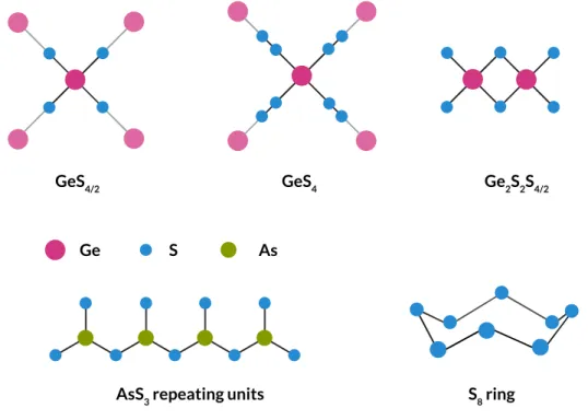
Figure 2.2: Schematic illustrations showing some of the key structural units making up ternary
(above) and binary (below) chalcogenide glasses.
2.3 Optical Properties of ChGs
The optical band gap of ChGs lies in the visible or near-IR regions as the inter-atomic bonds are typically weaker than in oxide glasses. ChGs are composed of heavier atoms when compared to oxide glasses and exhibit low bond vibration energies and low phonon energies. This enables excellent transparency in the infrared wavelength regime that covers the characteristic absorption peaks of several chemical and biological species. However, ChGs still exhibit impurity and electronic absorption, which will be discussed in section 2.4. Although the weak bonding and heavy constituents make them excellent for mid- and
far-GeS4/2 GeS4 Ge2S2S4/2
AsS3 repeating units S8 ring
IR applications, other physical properties such as glass transition temperature (Tg),
hardness, strength, and overall robustness tend to be lower than oxide glasses. Their relatively high densities and high polarizability endow ChGs with high linear refractive indices (n = 2–3 depending on composition).
In addition to their excellent IR transparency, ChGs have also attracted attention due to their high Kerr (3rd order) nonlinearity that can be up to three orders of magnitude
higher than that of silica62, 63 and derives from electronic processes with an ultra-short time
scale of < 50 fs64 rather than free electrons with lifetimes on the order of nanoseconds. A
nuclear contribution to the nonlinearity on the order of 12–13% has also been demonstrated65. Nonlinear absorption processes such as multi-photon absorption (multiple
photons are absorbed to create an electron-hole pair) also occur in ChGs. Two-photon absorption (TPA) can lead to optical losses as the optical attenuation is now defined as 𝑑𝐼 𝑑𝑧⁄ = −𝛼𝐼 − 𝛼2𝐼2 where α
2 is the TPA coefficient. ChGs tend to exhibit low TPA66
which makes them excellent candidates for nonlinear applications as the figure-of-merit (FOM) for comparing nonlinear materials is defined as the ratio of the Kerr nonlinearity and the TPA coefficient62, 63.
ChGs exhibit several photo-induced phenomena due to their structural flexibility and their high-lying lone-pair p states in their valence bands63. A photo-induced change in the
refractive index connected to an optical band edge shift leading to an absorption change is observed when light of energy close to the band gap is incident on ChGs67-70. The refractive
index change can be either positive or negative depending on the dominant mechanism: photodarkening leads to an increase in the index while photo-volume expansion leads to a decrease in the index. Photodarkening is a process in which the optical band gap of the ChG material decreases upon illumination due to a red shift in the absorption edge and it can occur together with photo-volume expansion. Many models have been proposed in
literature to explain this phenomenon, but they can generally be categorized into one of the following structural changes71-78:
bond-breaking and rearrangement
changes in interlayer distances due to a weakening of van der Waals forces (can lead to photo-volume expansion)
photo-induced polymerization processes
Although photosensitivity effects are most prominent under near-band gap illumination, they have been observed at longer wavelengths (e.g., 1550 nm) by using resonators for cavity enhancement in As2S3 glass79. Since the energy is below band gap,
sub-gap defect absorption (Urbach band tail, mid-sub-gap states, etc.) is believed to be responsible for photosensitivity at longer wavelengths. Photosensitivity of ChGs has been exploited for a number of applications including direct writing of device features80-82 and changing the
response of microring resonators to ease fabrication tolerances83. The latter technique
enables the correction of the response of devices to match required specifications more closely (see Chapter 5). It is possible to reverse light-induced effects by annealing near the glass transition temperature.
2.4 Loss mechanisms in ChGs
Chalcogenide glasses are composed of heavier atoms when compared to oxide glasses and exhibit low bond vibration energies and low phonon energies. This enables excellent transparency in the infrared wavelength regime, which covers the characteristic absorption peaks of several chemical and biological species. To fully analyze the optical transparency of ChGs, we need to investigate their loss mechanisms. Optical loss reduction is a device performance necessity for the systems used as sensors since it enables a longer optical path inside resonant cavities (higher Q-factor). This allows the light to interact over a longer
time with the molecular species of interest, thus improving detection sensitivity. Quantitative analysis has revealed that low overall optical loss (~0.1 dB/cm) is the key to high detection sensitivity up to a point where temperature fluctuation noise starts to take over12, 14, 84.
There are typically three main optical loss mechanisms in planar ChG devices: radiative loss, roughness scattering, and material attenuation. Radiative loss refers to optical loss due to coupling into radiative or substrate modes caused by waveguide bending or quantum tunneling through a finite cladding thickness. This loss mechanism can be significantly reduced by an appropriate choice of device geometry. Scattering loss arises from roughness at the sidewalls of fabricated devices when the optical mode traveling through the device overlaps with the sidewall. Material attenuation can be further categorized into extrinsic loss due to impurity absorption and intrinsic loss which includes electronic absorption by band tail or mid-gap states (nonlinear absorption neglected at low power), Rayleigh scattering caused by statistical density fluctuations, and phonon absorption. In the mid- and far-IR regimes, Rayleigh scattering is negligible as the wavelength is much larger than the length scale of density fluctuations. Phonon absorption depends on characteristic bond vibration frequencies and can be avoided by appropriate selection of ChG composition. This leaves electronic absorption and impurity absorption as the major contributors.
Impurity loss has been relatively well examined in ChG optical fibers85-87, but similar
investigations with thin films have been scarce. Despite the high purity of the starting materials used, impurities contributing to absorption are still present unless specific purification procedures are carried out on raw materials (e.g., pyrolysis of sulfur) or during the melting process by including gettering materials such as magnesium for oxygen removal and metal chlorides for hydrogen removal88. If gettering is carried out solely to remove
increasing their peak strengths as shown. In Chapter 5, we will see that the contribution of impurity absorption loss is typically smaller than roughness scattering. However, removing these impurities may be crucial in few situations such as for sensing applications, where impurity absorption peaks may overlap with absorption peaks from chemical species of interest and contribute false signals. In addition, impurity absorption peaks can increase total loss over specific wavelength ranges making it difficult to achieve low device propagation losses.
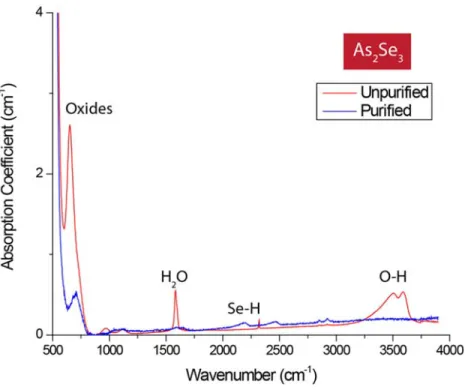
Figure 2.3: FTIR absorption spectra showing the effect of purification techniques on bulk As2Se3 glass. By gettering the hydrogen and oxygen impurities, absorption features attributed to H2O and
O-H vibrations are significantly reduced89.
Based on literature data showing oxygen, carbon, and hydrogen as the main impurities in bulk ChGs43, 87, 88, 90, we carried out preliminary studies to assess the impact of thin film
processing on impurity incorporation. Figure 2.4 shows oxygen, carbon, and hydrogen impurity concentrations in thermally evaporated thin films (~500 nm) and bulk samples taken from the same batch of Ge23Sb7S70 and As2S3 glasses, measured using Secondary Ion
Mass Spectroscopy (SIMS). It is clear that while carbon and hydrogen concentrations are quite similar in film and bulk, oxygen concentration in the Ge23Sb7S70 film is higher by
almost 7-fold as compared to bulk, suggesting that residual oxygen in the high-vacuum chamber may have been incorporated into the film during deposition. The higher oxygen concentration can lead to higher mid-IR device losses, as the optical loss from the O-H absorption band (centered at 2.9 µm) is correspondingly higher. It is possible to reduce the oxygen present in the evaporation chamber by use of a gettering pump91 or by distilling the
glass during bulk synthesis; as few additional C and H impurities are introduced into the film, simply starting with purified raw materials can reduce their concentrations92, 93.
Figure 2.4: Secondary Ion Mass Spectroscopy (SIMS) data collected on bulk glass and thin films
showing concentrations of common impurities such as oxygen, hydrogen, and carbon prior to any purification techniques.
Electronic absorption in amorphous materials such as ChGs is caused by mid-gap states arising from dangling bonds and band tailing of the density of states due to fluctuations in structural order94, 95. Their density may be controlled either by selective addition of chemical
modifiers that reduce the Urbach tail96, 97 or by modification of the chemical composition to
increase the band gap. However, such modifications might lead to changes in the thermal
Oxygen(O) Hydrogen(H) Carbon(C) 1015 1016 1017 1018 1019 1020 Co n ce n tr at io n (c m -3) Bulk Thin Film Ge23Sb7S70 As2S3
Oxygen(O) Hydrogen(H) Carbon (C) 1015 1016 1017 1018 1019 1020 Co n ce n tr at io n (c m -3) Bulk Thin FIlm (a) (b)
and optical properties of these glasses and have to be taken into account when designing planar microphotonic devices.
2.5 Chalcogenide glass processing
2.5.1 Bulk glass synthesisBulk ChG preparation involves a traditional melt-quench technique66, 98 starting with high
purity (99.999%) elemental constituents batched according to the composition required. The batched materials are vacuum-sealed inside a clean quartz ampoule free of larger impurities and moisture. The sealed ampoules are then heated at a temperature of several hundred degrees Celsius (dependent on specific composition) for several hours in a rocking furnace until the melt has homogenized. The ampoule is quenched in air to room temperature and returned to the furnace for annealing at sub-Tg temperatures to prevent
fracture of the ampoule and the bulk glass inside it.
Figure 2.5: The process of synthesizing bulk chalcogenide glass using a traditional melt-quench
technique. 2.5.2 Thin film processing and characterization
A number of deposition techniques have been used to fabricate thin films of ChGs including RF magnetron sputtering99, pulsed laser deposition (PLD)61, 100, chemical vapor deposition
(CVD)101, and spin coating of crushed glass dissolved in organic solvents such as
propylamine30, 102. In this project, the bulk ChG materials synthesized by our collaborators
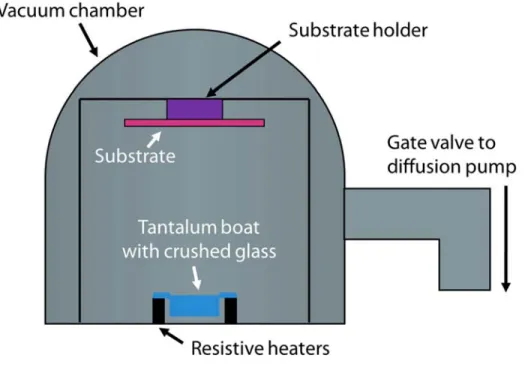
silicon substrates by single-source thermal evaporation from resistively heated tantalum boats under high vacuum (~10-6 – 10-7 Torr) as shown in Figure 2.6. Raw glass materials
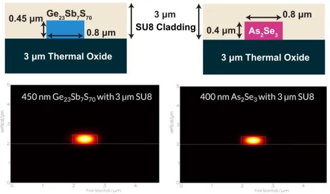
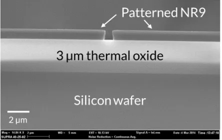
are prepared for evaporation by manually crushing them into small pieces ~1 mm in size using a mortar and pestle. Our planar device fabrication utilizes an ultraviolet photolithography process with a negative photoresist followed by thermal evaporation and photoresist lift-off in acetone (under sonication) to form patterned structures14 (see Chapter
4). The photosensitivity of ChGs has also been exploited for fabrication by using femtosecond laser pulses to write patterns directly80, 103 into ChG films.
Figure 2.6: Schematic illustration of the thermal evaporator setup used for deposition of
chalcogenide glass and PbTe films.
We analyze the deposited thin films by first evaluating their composition using Wavelength Dispersive Spectroscopy (WDS). This technique has demonstrated good agreement with bulk stoichiometry for our thin films (~500 nm) but cross-sectional measurements on thicker films of ternary glasses exhibit deviation from bulk stoichiometry
with increasing thickness. Thick films show a closer match to bulk stoichiometry at the bottom of the film than at the surface. We can attribute this to the different vapor pressures of the elements in ternary systems that lead to different rates of evaporation and a gradual change in the stoichiometry of glass material left in the evaporation boat. One way to address this issue is by starting out with a different composition such that the film composition is more closely matched to the target stoichiometry. Our measurements on binary chalcogenides such as As2S3 and As2Se3 showed more uniform stoichiometry across
varying thicknesses46.
Table 2.1: Wavelength Dispersive Spectroscopy (WDS) measurements on evaporated Ge23Sb7S70 films demonstrate that thicker films tend to deviate further from the bulk composition when measured at the top surface.
Thickness Average Atomic %
Ge Sb S 0.4 µm 22.7 9.0 68.3 1.3 µm 18.9 11.0 70.1 3.7 µm 13.8 7.7 78.5 4.2 µm 14.7 7.7 77.6 Bulk 23 7 70
We have also evaluated Ge23Sb7S70 thin films deposited by spin-coating and compared
their stoichiometry to those deposited by thermal evaporation. Chalcogenide glasses are soluble in select organic solvents such as ethanoldiamine (EDA) and the solution can then be spin-coated on a substrate to create thin films. The residual solvent in the film is driven out through a baking process in a vacuum oven to obtain uniform films of ChG materials102.
Table 2.2: WDS composition data for spin coated Ge23Sb7S70 films showing large deviation from bulk stoichiometry. We note an excess of germanium and a sulfur deficiency, even when compared to evaporated thin films.
Thickness Average Atomic %
Ge Sb S
321 nm 36.24 10.41 53.35
264 nm 33.57 9.8 56.63
201 nm 29.64 8.5 61.85
177 nm 29.81 8.62 61.57
Figure 2.7: Ellipsometry data (n, k) collected from thin films of Ge23Sb7S70 (Left) and As2Se3 (Right) deposited on 1 cm diameter CaF2 substrates.
We measured the complex refractive index of thin films made from two of our glass compositions via a variable angle spectroscopic ellipsometry technique (performed at J. A. Woollam, Inc.). The real and imaginary parts of the refractive index were measured over a broad wavelength range and the results are plotted in Figure 2.7. The data shows that Ge23Sb7S70 has a refractive index of about 2.15 in the near- and mid-IR wavelength ranges
with low absorption coefficient. As2Se3 is a higher index material and its refractive index is
about 2.75 over the range of interest. These values are slightly lower than their bulk
0 10 20 30 40 1.2 1.4 1.6 1.8 2.0 2.2 2.4 2.6 2.8 3.0 Index of Refraction ExtinctionCoefficient Wavelength (μm) In d ex o fR efr ac ti o n (n ) 0.0 0.2 0.4 0.6 0.8 1.0 1.2 1.4 1.6 Ex ti n cti o n C o effi ci en t (k ) Index of Refraction ExtinctionCoefficient 0 10 20 30 40 1.0 1.5 2.0 2.5 3.0 3.5 Wavelength (μm) In d ex o fR ef ra ct io n (n ) 0.0 0.2 0.4 0.6 0.8 1.0 1.2 1.4 1.6 1.8 2.0 Ex ti n cti o n C o effi ci en t (k ) Ge23Sb7S70 As2Se3
counterparts61, 104, 105 indicating a different structural arrangement in the films and a reduced
density.
2.6 Effects of radiation on ChG materials
Part of this thesis work was dedicated to understanding the radiation hardness of chalcogenide glass materials as we anticipate remote chemical sensors may be deployed in harsh environments such as those near nuclear facilities. Past literature on this subject has studied various ChG compositions in bulk form and found that relatively high radiation doses (a few MGy of gamma) are required before any measurable changes occur106. Further,
many radiation-induced defects tend to be transient in nature and do not survive long-term107. The amorphous nature of our glass materials makes it harder to characterize defects
introduced by radiation when compared with their crystalline counterparts. However, we can categorize defects in these materials into the following types107-112:
structural defects such as dangling bonds and abnormal bonding configurations.
deviation from stoichiometry
presence of impurities that disrupt the glass network and interact with glass constituents (oxidation, hydrogenation, carbonization, etc.)
All of these defects are more likely to be present in thin films as the overall structure of films tends to deviate from the bulk based on how a given glass melts and evaporates. For instance, As2S3 glass tends to evaporate primarily as molecular units of As4S4 and
consequently the film has a much different structure than the bulk, which is made up of repeating units of As-S3 with one of the sulfur atoms bridging adjacent units. The defects
can affect the thermal, optical, and microstructural properties of chalcogenide glasses and when present in sufficient numbers can be measured using common techniques such as
Raman spectroscopy, differential scanning calorimetry, and UV-Vis spectroscopy107, 112.
Exposure to radiation can create more of these defects through bond breakage and bond-switching reactions, as illustrated schematically in Figure 2.8a and Figure 2.8b respectively for As2Se3.
Figure 2.8: (a) Bond breakage leading to non-bridging anions; (b) coordination topological
defects from bond-switching reactions upon irradiation.
We have measured the UV-Vis spectra of Ge23Sb7S70 and As2Se3 bulk and thin films
before and after irradiation with a dose of 5×1015 cm-2 alpha particles with 3 MeV energy
at a grazing angle incidence (implanted at the Pacific Northwest National Laboratory). First, we observe that the Ge23Sb7S70 bulk sample does not exhibit any appreciable change
in the absorbance or the wavelength of the absorption edge post-irradiation. The As2Se3
bulk sample does show a slightly higher absorbance but it returns to the pre-irradiation level when the sample is measured again after one month. With the thermally evaporated thin films, Ge23Sb7S70 once again does not exhibit much difference after irradiation, possibly
indicating a relatively high degree of radiation hardness. The As2Se3 film appears to have
two absorption edges with a plateau in between them after irradiation. This could be indicative of the formation of a secondary phase with a different bandgap or voids in the films. As we used soda-lime glass slides as our thin film substrates, it is conceivable that
the absorption edge at the lower wavelength is from the substrate due to through-thickness voids in the film. The spectrum also appears to be returning to the pre-irradiation state after a month, demonstrating that many of the defects created by irradiation are transient in nature. Since there is a time delay of a few days between irradiation of the samples and their measurement due to shipping, it may be possible to observe a larger change in irradiated samples if data is collected soon after radiation exposure.
Figure 2.9: UV-Vis transmission spectra of Ge23Sb7S70 and As2Se3 bulk glass (Left) and thermally evaporated thin films (Right) before and after alpha irradiation. In both cases, As2Se3 shows higher sensitivity to the radiation damage, including a possible second phase or voids formation for the thin film. In all cases, measurements done after a month show relaxation towards original
state, indicating the transient nature of radiation-induced defects.
In Figure 2.10, we observe that the As2Se3 films do indeed exhibit the formation of voids/air
holes after alpha irradiation, which may explain the plateau in the UV/Vis spectra. By comparison, our measurements on Ge23Sb7S70 films show a much lower degree of void
formation and hence their UV/Vis spectra remain unchanged post-irradiation. This data shows us that the As2Se3 films are more sensitive to radiation damage than the Ge23Sb7S70
Figure 2.10: Optical microscope images showing holes and delamination in alpha-irradiated
As2Se3 films. These defects could be responsible for the plateau seen in the UV-Vis sepctra.
2.6.1 Position annihilation lifetime spectroscopy
Positron annihilation lifetime spectroscopy (PALS) is a nondestructive technique to probe defects in materials on an atomic scale. A beam of positrons is implanted into the material under test and the time elapsed until their annihilation through interaction with electrons is measured by detecting the radiation emitted upon annihilation. When defects such as vacancies are present in a material, positrons are trapped in them and their lifetime increases. By comparing annihilation lifetimes of irradiated and non-irradiated samples, it should be possible to begin gaining an understanding of the nature of defects induced by radiation. One caveat is that the amorphous materials we will test already have defects and so the change after irradiation could be very small and hard to measure.
Our first set of measurements were carried out at Opole University in Poland on non-irradiated films to determine whether PALS would yield meaningful data for bulk and thin
film samples of As2Se3. From our UV/Vis data, we noted that this glass composition was
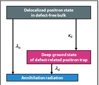
more sensitive to alpha irradiation and we chose it for PALS measurements as well. Due to a low fraction of positrons annihilating in the film compare to the Si substrate we are not able to unambiguously decompose the various contributions from the films. Hence, we analyze them as an average contribution from all possible defects within the two-state positron-trapping model. Figure 2.11 shows a schematic of the two-state positron-trapping model. A positron entering the sample can either (i) annihilate by combining with an electron in the defect-free bulk to emit radiation with rate b, or (ii) move from a delocalized
state in defect-free bulk to a defect-trap state with a defect trapping rate of d and then
annihilate at a later time with rate d. For both spin-coated and thermally evaporated thin
films, the fraction of positrons annihilated within the film was less than 3%.
Table 2.3: PALS parameters for spin-coated films Sample av (ns) d As2Se3 bulk 0.262 0.71 2.8 µm film 0.314 1.41 0.88 µm film 0.384 2.03 0.46 µm film 0.460 2.45
Table 2.4: PALS parameters for thermally evaporated films
Sample av (ns) d
As2Se3 bulk 0.262 0.71
1.98 µm film 0.300 1.28
0.77 µm film 0.352 1.78
0.43 µm film 0.425 2.29
Based on the initial PALS measurement results, we can make a few preliminary conclusions. The average positron lifetime (av) decreases as thickness increases towards the bulk
sample, which corresponds to a general trend in free volume (density) of these samples.
A higher defect-trapping rate (d) is observed as the thickness of the films goes down.
The greater the thickness, the closer the PALS parameters are to the bulk sample.
Spin-coated films possibly have more defects capable of trapping positrons than thermally evaporated ones do.
If radiation-induced effects are large enough, we can detect them through changes in
d or in the parameters of second channel of annihilation.
We have fabricated more bulk glass and thermally evaporated thin films of As2Se3 and
exposed them to gamma radiation doses of about 220 Mrad (2.2 MGy) using a 60Co source
while placed inside vacuum-sealed quartz ampoules to reduce ozone formation. The samples were sent to Opole University for measurement immediately after removal from the irradiator to ensure that we can observe the effects of transient defects before they decay.
2.7 Other mid-IR transparent materials
Group IV elemental compounds silicon and germanium are excellent mid-IR candidates due to their high refractive indices and the ability to use single-crystal layers to fabricate microphotonic devices. Silicon-on-insulator (SOI) technology has been widely used in the telecom wavelength range and many research efforts have focused on doing the same for the mid-IR17, 19, 113. Germanium grown on silicon substrates has also been demonstrated as a
mid-IR platform114-116. Our own work on silicon-based materials systems has yielded multiple
successful mid-IR technologies:
Silicon devices on silicon dioxide pedestals117: the oxide is isotropically
etched to form an undercut pedestal. This structure reduces mode overlap with the oxide undercladding and enables transmission at wavelengths where the oxide would begin to show absorption.
Silicon devices on silicon pedestals118: the silicon beneath the waveguide
layer is etched once more and this type of structure can be built directly on a silicon wafer, reducing complexity and eliminating any potential issues with other materials.
Silicon nitride devices on oxide38: thick, silicon-rich nitride films were
grown using CVD and then etched to create mid-IR waveguides.
2.8 Summary
In this chapter, we have looked at chalcogenide glass materials and their suitability for infrared photonics applications due to their wide transparency window. Chalcogenide glasses are easy to fabricate (bulk and thin film) and their compositional flexibility allows tuning of optical properties such as refractive index. Further, material attenuation in ChG materials arises due to the presence of impurities in the raw materials and defects in the glass network. We have also performed UV/Vis and PALS measurements to gain a preliminary understanding of the defects induced by alpha radiation in ChG bulk and thin film samples. The As2Se3 samples show higher sensitivity to radiation damage but defects
in ChG materials tend to be transient and further measurements are required. We discuss waveguides, resonators, and designs for near- and mid-IR devices in the next chapter.
Chapter 3:
Waveguides and Resonators
At the component level, passive waveguides and optical resonators constitute the key microphotonic elements for a number of on-chip applications such as telecommunications, optical interconnects, and most importantly, mid-IR sensing and spectroscopy. Waveguide sensors can transmit a wider wavelength range and hence are useful for fingerprinting across the entire mid-IR regime. Resonator sensors with a large quality (Q) factor can offer very high sensitivity to changes in the complex refractive index12, 13, 15, 16. The long optical path
length in a resonant cavity leads to higher sensitivity from enhanced photon-matter interactions due to spatial light confinement over a longer period of time. In addition, it is feasible to fabricate resonator arrays that can be used for parallelized detection of multiple species while maintaining a small footprint. A good bio/chemical sensor must meet the criteria of (i) optical transparency in the mid-infrared wavelength range, (ii) high sensitivity, and (iii) high specificity all on an integrated silicon platform. In this chapter, we focus on the operating principles and design of dielectric waveguides and microresonators as the photonic elements of choice for this thesis work.
3.1 Dielectric waveguides
Waveguides are optical devices comprised of a higher refractive index core surrounded by a cladding material of lower index and light propagates through them via total internal reflection. Optical fibers, widely used in telecommunications applications, are an example of waveguides on a macroscopic scale. In this thesis, however, our focus is on waveguides fabricated on silicon substrates for microphotonics applications. When the waveguides comprise a higher index thin film on a lower index substrate, they are called slab waveguides and light is only confined along a single direction. Strip waveguides, as the name implies,
contain a narrow strip of the higher index material on a lower index substrate and confine light in both directions perpendicular to the propagation direction. A ridge waveguide combines the two types by placing a strip of the higher index material on a slab of the same material. Light is confined in two directions and the larger size confines light towards the center, which helps reduce scattering losses from the waveguide sidewalls. Figure 3.1 shows a schematic of the three main types of waveguides. Our emphasis this thesis is on strip waveguides.
Figure 3.1: Schematic showing the three main types of waveguides. The waveguide core is
comprised of a higher index material than the undercladding to confine the mode spatially. The work presented in this thesis uses strip (or channel) waveguides.
A time-invariant, stable electromagnetic field pattern that is an eigensolution to Maxwell’s equations is referred to as an optical mode. A guided mode (in a waveguide) is a stable amplitude and polarization profile in which the wave propagates at a given wavelength. The field profile of a given mode is determined entirely by the geometry and the refractive indices of the materials comprising the waveguide at the wavelength of interest. The geometry and indices also describe the effective refractive index (neff) of the
propagating mode that is defined by the ratio of the velocity of light in vacuum and the phase velocity in the waveguide. The effective index is always less than the index of the waveguide core and greater than the index of the cladding. It is also related to the propagation constant,, by the equation neff = /2 where is the free-space wavelength.
Slab Waveguide Strip Waveguide Ridge Waveguide
While the effective index defines the mode index (higher neff = lower mode order), the
polarization of the mode determines which direction the electric and magnetic fields are oriented with respect to the direction of propagation. In a transverse electric (TE) mode, the electric field oscillates parallel to the substrate and perpendicular to the direction of propagation. Similarly, a transverse magnetic (TM) is defined by a magnetic field oscillating parallel to the substrate and perpendicular to the propagation (see Figure 3.2).
Figure 3.2: TE (Left) and TM (Right) propagation modes in a slab waveguide. The electric
field in the TE mode and the magnetic field in the TM mode are oscillating along the X-axis as the mode travels in the Z direction1.
Finally, the power confinement factor (Γ) is the ratio of the power confined within the waveguide core to the total power propagating through the structure119. The power is
calculated as the integral of the Poynting vector as shown in Eqn (2). When the refractive index contrast between the core and cladding is high, the power confined within the core is correspondingly high. For sensing applications, we desire a small fraction of the mode to be present outside the waveguide as it leads to greater overlap with any chemical species that encounter the device.
Γcore =∫ 𝑃𝑧(𝑠). 𝑑𝑠 𝑐𝑜𝑟𝑒 ∫∞𝑃𝑧(𝑠). 𝑑𝑠 (2) Y Z E Y Z H TE TM Ey = 0, Ex ≠ 0 Hy = 0, Hx ≠ 0
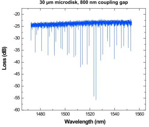
3.2 Dielectric microresonators
Optical resonators, or resonant cavities, are devices in which light can interfere constructively and be confined at resonant frequencies that are defined by the resonance condition defined as rN = neffL where r is the resonant wavelength, neff is the effective
refractive index, L is the cavity length, and N is an integer referred to as the mode order. When the light meets the resonant condition of a resonator, there is an enhancement in the optical power when the light is confined, completing a higher number of round trips than it would at other frequencies. Due to their frequency selectivity, resonators have found widespread use in applications ranging from optical filtering, laser cavities, nonlinear optics, optical switching, and chem-bio sensing120.
Figure 3.3: A few common types of resonator structures. The Fabry-Pérot cavity consists of
two highly reflective mirrors between which light can travel and is the simplest resonator structure. The microdisk, microring, and microsphere resonators all require a bus waveguide to
couple light into them. Fibers are typically used for microspheres.
A multitude of resonator configurations is in active use in research and commercial applications, as illustrated schematically in Figure 3.3. The simplest resonator device is a Fabry-Pérot structure that uses two parallel planar mirrors to form a low-loss cavity in which light is repeatedly reflected back and forth. Our research relies on dielectric
Microdisk Resonator Microring Resonator Microsphere Resonator
Bus Waveguide
Coupling Gap
Fabry-Pérot Cavity Mirrors