Dislocation Engineering in InAlGaAs/SiGe Alloy Systems
for Heteroepitaxial Integration
by Rushabh Shah
Bachelor of Technology in Engineering Physics Indian Institute of Technology Guwahati, 2012
Submitted to the Department of Materials Science and Engineering in Partial Fulfillment of the Requirements for the Degree of
Doctor of Philosophy in Materials Science and Engineering at the
MASSACHUSETTS INSTITUTE OF TECHNOLOGY February 2019
C
2019 Massachusetts Institute of Technology. All rights reserved.Signature redacted
Signature of Author:Department of Materials Science and Engineering December 27, 2018
Signature redacted
Certified by:
4-0pFl' Eugene A. Fitzgerald
Merton C. Flemings-SMA Professor of Materials Science and Engineering
Signature redacted
Thesis Supervisor
Accepted by:
MASSACHUSETTS INSTIUTE
/
Donald R. SadowayDislocation engineering in InAlGaAs/SiGe alloy
systems for heteroepitaxial integration
Abstract
Semiconductor devices based on GaAs substrates use III-V alloy systems like Inx(AlyGa,_y)iAs for optoelectronic devices and high frequency communication applications. Heteroepitaxial integration of such devices with Si has generated a lot of interest because it has the potential of combining the desired material properties with the low cost of the Si manufacturing platform and enabling
monolithic integration with Si CMOS, creating novel integrated circuits. However, heteroepitaxial integration introduces challenges related to detrimental crystal defects like dislocations that are created in the process and require buffer layers to accommodate such defects and minimize their impact on device performance. One buffer layer scheme that is receiving widespread adoption involves the direct growth of Ge on Si. It produces a threading dislocation density -2x10 7cm-2 but
this density is too high for applications like high efficiency GaAs solar cells.
In this work, we aim to study two methods that can reduce this defect density. One involves
developing a similar procedure to Ge on Si growth, for growing Ge on Si5oGe5o. We find that despite the lower lattice mismatch and availability of pre-existing mobile dislocations in this approach, the Ge film retains a high metastable strain that generates a high density of crystal defects.
The second method involves the use of low x In,(AlyGa,_y)1 As buffer layers that use compressive strain to encourage dislocation reactions and drive dislocations to sinks (mesa sidewalls). Filtering effects lead to a reduced threading dislocation density, the lowest measured in this study is
7x106cm-2, but these effects do not scale with x, showing that dislocation sources are active and play
an important role. These films have residual tension due to differences in coefficient of thermal expansion with Si substrates. Recombination enhanced dislocation glide effects permit direct visualization of processes that operate to relive this residual strain at room temperature, in
cathodoluminescence imagining conditions. This provides a first estimate of density of dislocation sources and interaction probability between dislocations under residual strain conditions.
Unexpected dark line defects were observed in cathodoluminescence imaging and the use of "overshoot layer" was demonstrated to be critical in reducing their density.
Preliminary work towards processing photovoltaic cells and a layer transfer method that involves wafer bonding for reuse of buffer layers is also discussed.
Table of Contents
List of Figures ... 7
List of Tables...11
A cknow ledgem ents...13
C hapter 1 Introduction...15
1.1. M otivation ... 15
1.2. Buffer layers in lattice m ism atched epitaxy ... 15
1.3. O rganization of thesis...18
Chapter 2 Strain relaxation of germanium on relaxed Si5oGe5o buffers on silicon substrates ... 21
2.1. Introduction ... 21
2.2. Experim ents...2 1 2.3. R esults and D iscussion ... 23
2.4. C onclusion...32
Chapter 3 Dislocation dynamics in low misfit Inx(AlyGai-y)1 As films grown on relaxed Ge buffer layers on silicon substrates...35
3.1. Introduction ... 35
3.2. Experim ental details...36
3.3. Recombination Enhanced Dislocation Glide (REDG)... 41
3.4. D ark Line D efects...52
Chapter 4 Towards Photovoltaic Cell Processing and Heterobonding layer transfer...73
4.1. M icro optical spectrum splitting lateral multijunction ... 73
4.2. Layer transfer by direct wafer bonding and sacrificial layer etch ... 75
Chapter 5 Conclusion ... 81
5.1. Sum m ary of results...81
5.2. Recom m endations for future work ... 82
Appendix A. Process Flow for G aAs PV cell processing...85
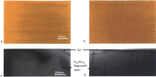
List of Figures
Figure 1-1 Schematic of the two Ge buffer layers schemes. (a) Graded layers distribute MD over a volume to achieve very long MD lengths and hence few TDs reach the surface. (b) Two-step Ge growth, a high density of TD segments are initially formed that are reduced later by process like thermal cyclic annealing. Device layers (like GaAs) are grown on top of such buffer layers...16 Figure 1-2 Sensitivity of GaAs solar cell performance to threading dislocation density from reference [1 1]...1 8 Figure 2-1. lumxlum AFM scans for samples S1 (a), S3 (b), S5 (c). The rms roughness is low and all samples have features with peak-valley amplitude 1nm-3nm with spatial wavelengths of 10-30nm..23 Figure 2-2 Effect of initial dislocation density on hillock density for S5. The hillock density in (a) and the XTEM of the low pt Si5oGe5o regrowth layer are representative of all the samples studied. (b)
shows a significantly higher density (>108cm2) when S5 recipe is repeated on a Si
5oGe5o buffer created with a high dislocation density as shown in (d) ... 24 Figure 2-3 lumxlum AFM scans for samples for processing and growth at 500C. S3 (a), S5 (b) remain planar after ex situ annealing but S8 (c) and S9(d) show 3D island have formed. ... 25 Figure 2-4 ECCI imaging under a "3 beam condition" revealing misfit dislocations in the primary slip system at the Ge/Si5oGe5o interface for samples S3 (a) and S5(b)...26 Figure 2-5 ECCI images of sample S4. (a) shows a "y-center" defect and (b) shows a change in contrast at in intersection of orthogonal dislocations indicating that edge dislocations are formed by cro ss slip ... 2 7 Figure 2-6 004 Reciprocal space maps of S6 and S7 used to measure the residual strain in the Ge film . ... 2 8 Figure 2-7 a) Dark field image of sample S6 tilted to a 2 beam condition with g=(022) revealing planar defects in a (111) plane. b) Bright field image of sample S7 tilted to a 2 beam condition with g=(022) revealing planar defects in a (111) plane. The fringes near the surface are due to the high tilt deviation from the (110) zone axis... 29 Figure 2-8 a) Residual film measured for the as grown sample and after ex-situ annealing. For
residual strains < 1.8x10², XRD was used and for higher residual strains ECCI used to calculate the
misfit length. (b) shows how the defect density increases with thickness. For the S6 and S7 (thicknesses 46nm and 97nm), an order of magnitude estimate is made on the basis of their
Figure 2-9 ECCI imaging under a "3 beam condition" revealing misfit dislocations in the primary as well as secondary slip system at the Ge/SioGeo interface for samples S3 (a) and S4(b) after furnace an n ealin g ... 30 Figure 2-10 X-TEM of samples S4 (a) and S5(b) after furnace annealing. ... 31 Figure 2-11 Processing paths for producing strain relaxed Ge films on Si substrates. I- graded buffer.;II- low temperature (IHa) -high temperature (jIb) growth on Si followed by cyclic annealing (Ic); III growth on relaxed Si5oGe5o buffer layer in this work...32 Figure 3-1 Schematic of the different layers of the samples studied in this chapter...37 Figure 3-2 Schematic depicting the interpretation of defects at different depths from the surface for cathodolum inesce m ap s...39 Figure 3-3 Dislocation velocities in n-GaAs measured with and without electron beam excitation at different temperatures as reported by Meada and Takeuchi [45]. ... 42 Figure 3-4 CL images taken at different instances of the exposure of a fixed area. The circle in a-c moving left is a fast moving dark spot. The circle in d-f is a slow moving dark spot. The 3 ellipses
depict events that are described as a source type (c) in the following section... 43 Figure 3-5: A histogram of measured velocities under irradiation of a 5kV electron beam with
current density 1.2A/m2. The x-axis values correspond to upper limits of a range of velocities
corresp on ding to a bin ... 43 Figure 3-6 Events showing a) non reacting interaction, b) fusion reaction and c) annihilation reaction between threading dislocations. Each image height is 6um...45 Figure 3-7 Operation of source type (a). Two additional dark spots are created at the site of an immobile dark spot that move in opposite directions with different velocities along directions close to [1 1 0]...4 6 Figure 3-8 Operation of source type (b). Two dark spots are created in a clear region, that move in opposite directions with different velocities along directions close to [110]... 46 Figure 3-9 A mobile dark spot is emitted from an immobile dark spot, moving along [110], and a transient segm ent connecting the two is observed. ... 46 Figure 3-10 A dark line defect segments contracts with the motion of one dark spot along its length and another m oves in the opposite direction ... 47 Figure 3-11 Possible reconstruction of the CL signature observed corresponding to source type (c) in the double heterostructure layers. The blue intermediate layer corresponds to the active layer. The solid line denotes the im m obile dark spot... 51
Figure 3-12. CL Line defects measured at room temperature using a pan-CL detector. Samples M3 (a), M4 (b) and M5 (c) have identical double heterostructure grown on different buffer layers...53 Figure 3-13: CL map of sample M3. A) room temperature pan-CL. b) 10K top cladding layer
em ission m ap c) 10K active layer em ission m ap ... 54 Figure 3-14. Terrace etch for characterizing depth distribution of defects using ECCI. An SE image is shown in a). The steps marked 1,4 and 9 are in the top cladding, active layer and the bottom
cladding layer respectively. ECCI image at step 4 is shown in (b) that shows threading dislocation contrast but no m isfit like dislocations are visible. ... 56 Figure 3-15 a) Dislocation line segment in the bottom cladding layer. (b) Threading dislocations visible in first scan of the surface. (c) Line defect becomes visible after repeated scanning. ... 57 Figure 3-16 a) Overlay of CL image, SE image during FIB preparation and corresponding BF-STEM image. (b) and (c) are expanded portions of the STEM image that show artefacts associated with m ultip licatio n so urces...58
Figure 3-17 Expected reduction in pt with increasing plastic strain relief Ep. ... 63 Figure 3-18 Threading dislocation density of uniform layers grown on substrate H.* correspond to aerial density of dislocations measured by ECCI and are plotted on the left axis. 0 denote 1/pt allowing easy com parison with the expected m odel... 64 Figure 3-19 Cross section TEM of 3703 tilted to a 2 beam condition with g=(220) to enhance
dislocation contrast. The Inso(A25Ga75)9oAs film thickness is 120nm ... 64 Figure 3-20: Threading dislocation density measured for graded buffers with terminal compositions
of 5%, 10% and 15 % In .The dashed line corresponds to the dislocation density of the virtual
substrate H . Error bars correspond to 3a... 65 Figure 3-21 Threading dislocation density measured for graded buffers with terminal compositions
of 3%, 5% and 9 % In .The dashed line corresponds to the dislocation density of the pre-threaded
substrate M . Error bars correspond to 3y ... 66 Figure 3-22 Effect of different buffer layers with identical In5(AlyGaiy)9 5As uniform layers on pt. The
open circles correspond to the right Y axis that shows calculated ,...67 Figure 3-23 Effect of mesa size on threading dislocation density for structure M3. The two data points for each mesa size in (a) represent measurements performed in different mesas, showing the mesa-mesa variability. (b) shows the same data as a function of perimeter/area ratio (x axis is
Figure 4-1:a) Prototype to test coupling of individual PV elements with optical elements and power management control systems. (b) Die layout of individual PV cell that allows positioning of the PV cell with respect to the spectrum splitting optical element...74 Figure 4-2 Process flow for PV diode fabrication ... 74 Figure 4-3 Process flow for layer transfer of pre patterned film using direct wafer bonding and
sacrificial etch ing ... 77
Figure 4-4 10umxlOum AFM scan of the bonding surface (a) before and (b) after CMP. ... 78 Figure 4-5 DIC images of mesas visible on the target substrate. (a) 25 urn mesa shows complete transfer (b) 100um mesa shows center to edge variations...79
List of Tables
Table 2.1 Film thicknesses for Ge grown at low temperature ... 22 Table 3.1 Details of the layers that together constitute the In,(Al25Ga75)1_,As epistack...37 Table 3.2 CL Dark line density measurements...53
Acknowledgements
My doctoral journey has taken well over 6 years but it does not feel nearly that long because of the support and company of many wonderful people.
I am very grateful to my advisor, Prof. Eugene Fitzgerald for providing this opportunity. Gene has given me a lot of freedom in navigating the journey while providing enough guidance and support that I would not get lost. In the many orders of magnitude of uncertainty inherent in the research world, it has been always been an assurance that Gene spends a lot of time thinking about "practical paths" to realization of the research in the group. Gene is very encouraging and approachable, both for matters relating to research and beyond. I am looking forward to hearing news from Singapore as he focuses his attention on SMART in a new phase of his career. I also thank my thesis
committee members, Prof. Kimerling and Prof. Thompson for their feedback and patience over the years.
I am fortunate to have two group alumni as mentors -Dr. Mayank Bulsara and Prof. Mukherjee. Mayank taught me a lot about both our CVD systems and helped me structure my early research goals. Collaboration with Prof. Mukherjee's group was critical in the past year and all the
cathodoluminesce imaging in this thesis was performed by his students, Eamonn Hughes and Connor Reilly.
Working with the Fitzgerald Group members -Prithu, Adam, Kunal, Tim, Ryan, Roger and Chris has been an absolute delight and is one of the highlights of my time here. The comradery stems
from collectively attending to the whims of the CVD reactors (which can take entire days to weeks at a time!), but extends outside the lab as well. Prithu can take uncertainty in stride -there was a lot of downtime in his final year. Adam showed me the ropes in MOCVD, XRD and TEM -the bread-and-butter of the work in the thesis. Kunal has patiently entertained many "raw" ideas I have discussed with him over the years, both as a lab mate and as a collaborator. Tim gets stuff done! And was a great and frequent host. Ryan Iutzi is really funny (read his thesis acknowledgements, even if you don't know him) and he enlivened the office. Roger was always there to help with the lab, even in the last few hectic months of his graduation when the group size was dwindling down. Chris has always been very dependable and has shouldered more than his share of lab
been running the lab with me over the past year. He has the herculean task of transitioning to a new phase of the lab, running it with a smaller team. But he has already demonstrated, several time over, that he is up for the job.
The work in this thesis relies heavily on the technical support of staff at CMSE MRL and MTL. Dennis Ward and Gary Riggott have directly contributed to the some of the work and have been very friendly and accommodating. Mark Beals's support has been instrumental in managing SEL. Since Lars Llorente joined us at 13, the building has gotten much safer.
Many thanks to all the friends who have made my stay in Boston memorable and fun. There is no way I can do justice to everyone here but I am especially indebted to Sanket, Himani and Ankur. They have never worked in the same or similar lab but by now, can understand my complaints about charcoal filters and "glassware". Finally, my parents and sister in India, who have no clue about the technical aspects of this work, have been a constant and limitless source of support. Throughout my education, they have gone the extra mile to give me better resources and I would not have reached this far had they done things differently. I am eternally grateful to them.
Chapter 1
Introduction
1.1. Motivation
Many commercially available semiconductor devices like red LEDs, high efficiency solar cells and
high frequency transistors used in wireless communication are based on GaAs substrates and use
III-V semiconductor alloys like Al.Ga,-As and InGa1 .P. A barrier to a more widespread application
of such devices is the high cost associated with the GaAs substrate and manufacturing process as
compared to that of Si based devices that are produced at a much larger scale. Integration of GaAs
based materials aims to get the best of both worlds; the unique material properties of III-V devices
with the low cost and large manufacturing platform of Si based microelectronics industry. High
efficiency solar cells, typically used in space applications are grown on GaAs or Ge substrates which
are expensive and can benefit from using cheaper, larger Si substrates. One encouraging path for
commercialization of integrated III-V devices with Si CMOS [1] also requires that the III-V devices
are grown at the scale of Si CMOS that cannot be done using native GaAs substrates. Integration of
III-V materials on Si by their direct growth has substantial challenges due to difference in lattice
constants, crystal structure and coefficient of thermal expansion, that lead to deleterious defects in
the II-V materials grown. There is a considerable body of literature [2], [3] devoted to the
understanding of these defects and methods used to manage the defects.
This research studies the defect structure of one such dislocation engineering scheme using
Inx(AlyGay)s-As/Si,-Ge2 buffer layer with the aim of enabling GaAs based devices like solar cells
on a Si platform.
1.2. Buffer layers in lattice mismatched epitaxy
techniques used for their mitigation. An epitaxial film with a different lattice constant than the substrate can be grown to mimic the in plane lattice constant of the substrate (pseudomorphically) only up to a certain thickness termed critical thickness. Beyond this thickness, plastic relaxation takes place by the introduction of dislocation defects that try to relive the strain at the film/substrate interface. A dislocation lying along the interface is termed a misfit dislocation (MD). These misfit dislocations do not continue from one edge to another but instead have segments connecting them to the surface, called threading dislocations (TD). Dislocation defects are detrimental to device performance; they degrade minority carrier lifetime which is crucial for devices like solar cells and LEDs and decrease carrier mobility that is important for devices like high frequency transistors. To minimize the deleterious effects of dislocations on devices, buffer layers are used in between the device and substrate. The purpose of the buffer layer is twofold; first, it aims to accommodate the necessary misfit dislocations so that they are not in the device layers and second, to minimize the number of threading dislocation defects that inevitably enter into the device region.
Ssi Low Temperature
CMX /
\X\
Si High Temperature , I CycllcArwnealIng b~ aFigure 1-1 Schematic of the two Ge buffer layers schemes. (a) Graded layers distribute MD over a volume to achieve very long MD lengths and hence few TDs reach the surface. (b) Two-step Ge growth, a high density of TD segments are initially formed that are reduced later by process like thermal cyclic annealing. Device layers (like GaAs) are grown on top of such buffer layers.
T
M 0
Si SI
Integrating GaAs-like materials on Si using Ge and Si1.Ge. buffer layers has the benefit of having a wide process window that does not create deleterious antiphase defects [4], [5] that can otherwise
occur due to differences in the crystal structure of the two materials. Two different approaches have shown some success in obtaining moderate threading dislocation density Ge layers on Si. One employs compositionally graded buffers (Figure 1-1a), where the lattice constant is changed gradually over some film thickness. The aim of this approach is to minimize the number of dislocation segments that need to be nucleated in order to relive the strain in the film. Optimally designed graded buffers [6] have very long misfit dislocation segments, distributed in the entire volume of the graded region. The other approach, termed "two step" growth [7] (Figure 1-1b), uses a low temperature growth to grow a thin Ge layer on Si that generates a very high density of
dislocations, relieving most of the strain. This is followed by a high temperature growth and annealing processes that leverage the difference in thermal expansion coefficients between Ge and Si, which allow the dislocations to react and reduce their density. Once the Ge layer is grown, GaAs can be grown with relative ease since their lattice constants are closely matched. If a larger lattice constant is desired, an additional graded buffer layer, can be used in an appropriate alloy system like
Inx(AlyGa,_y),_xAs.
Of the two buffer layer approaches described, graded buffers have demonstrated some of the lowest threading dislocation density (2x106cm2) GaAs films on Si [8] .However, the Si
1-Gex buffer used is actually a multistep growth with an intermediate chemical mechanical polishing step, making it a complex task to maintain process control of and is not currently research accessible. Currently, commercial vendors have established processes only to produce such buffers with a maximum of 50% Ge, although in principle, it is possible to develop buffers with 100% Ge. The two-step approach, produces a higher threading dislocation density (-2x107cm-2) [7], [9] but is a simpler
~~1
threading dislocation density of GaAs and InX(AlyGaY)IXAs layers will depend on the threading dislocation density of the Ge layer.
Calculated GaAs AMO Efficiency
25 20 15 Efficiency % 10 5 01.E+5 1.E+6 1.E+7 1.E+8
Substrate Dislocation Density
cm-2
Figure 1-2 Sensitivity of GaAs solar cell performance to threading dislocation density from reference [11].
Figure 1-2 shows the sensitivity of the efficiency of a GaAs solar cell design to threading dislocation
density. It can be seen that ideally, a threading dislocation density of 105cm2is desired as it has no impact on the solar cell efficiency, but even a threading dislocation density of ~106cm2 creates only a
small impact on performance. Since, the available Ge/Si buffer layer is of a higher density
(-2x107cm2) additional defect engineering is required to reduce the density of these defects in the
device layers.
1.3. Organization of thesis
This research aims to build upon the available Ge/Si and SisoGeso/Si platforms to produce low
defect density films that can be used for GaAs based devices. Chapter 2 combines the ideas for two
different buffer layer schemes used to produce Ge in developing a two-step growth process for Ge
on strain relaxed SisoGeso graded buffers. The strain relaxation and defect density in Ge for a kinetic
describes the effect of growing In,(AlyGa1y)iAs layer on top of Ge that have a small lattice
mismatch. The structure relieves compressive strain during its growth but is tensile strained at room
temperature due to differences in coefficient of thermal expansion. In characterizing such samples
with cathodoluminescence maps, recombination enhanced dislocation glide was observed for some
films, that allowed us to study dislocation interaction events and sources that are generally too rare
and sparse and hence not been studied before. Other than threading dislocations, line defects are
revealed in cathodoluninescence maps that have been characterized and growth strategies to
eliminate them are demonstrated. Next, we study the effect of the compressive strain relieved during
the growth of In,(AlyGa,-y)1 As on the threading dislocation density. Simple predictions of
dislocation interactions have predicted a significant decrease in dislocation density due to increase in
dislocation filtering effects (dislocation reactions or their motion to edges) but our results show that
such models are deficient in ignoring dislocation sources that play a significant role. In Chapter 4, preliminary work done towards establishing processes of fabrication of photovoltaic devices and a
layer transfer process that involves direct wafer bonding is described. Chapter 5 is a summary of the
Chapter 2
Strain relaxation of germanium on
relaxed SisoGeso buffers on silicon substrates
2.1. Introduction
Low threading dislocation density Ge on silicon substrates enable monolithic integration of silicon CMOS with high performing photodetectors [10] and GaAs based devices [12]. To obtain low defect densities, a thin layer is grown at low temperatures that undergoes 3D island growth followed by coalescence [13] to produce a thin smooth film with a very high density (> 10'4cm-2) of threading dislocations. The threading dislocation density (TDD) is reduced by annihilation and fusion reactions that take place as the film grows thicker and by performing various anneal processes [7],
[14], [15] that are thought to allow more reactions by the motion of threading dislocations as a response to the significant thermal expansion coefficient difference between Ge and Si [4]. This results in TDD of (1-2) 107cm-2 for films
-1-um
thick.The initial nucleation of dislocations is difficult to control due to the high lattice mismatch of 4% between that of silicon and germanium. It remains unclear if it is possible to reduce the number of nucleation events and obtain relaxed Ge with moderate dislocation density without employing additional high temperature annealing processes mentioned above. We study the strain relaxation of Ge films on strain relaxed Si5oGe5o buffers that have a reduced lattice mismatch of 2% having a moderate dislocation density in the buffer layer and its effects on nucleation of defects.
2.2. Experiments
Si5oGe5o strain relaxed graded buffers were prepared by Lawrence Semiconductors Research Lab on Silicon substrates with a surface normal miscut 6' from (001) with threading dislocation density pt in the range (7x10⁵-2x10⁶) cm2. Chemical Mechanical polishing was performed by Entrepix. Prior to growth, wafers are cleaned in a Piranha solution and the native oxide is striped in a 1:10 HF:H20 bath. The wafer is then loaded in a 1x6" Thomas Swan/Aixtron RPCVD with group IV capability. The precursors used are SiH and GeH for silicon and germanium respectively and the carrier gas is
hydrogen. First a 500nm Si5oGe5o regrowth layer is grown at 8250 C lattice matched to the Si5oGe5o substrates. The temperature is then lowered for germanium growth.
A series of Ge films were grown at a low growth temperature of 3800 C to suppress 3D island
growth. The sample thicknesses are listed in Table 2.1.
Table 2.1 Film thicknesses for Ge grown at low temperature
Sample ID S1 S2 S3 S4 S5 S6 S7
Thickness (nm) 6 10 13 16 26 46 97
Samples S3-S7 are annealed in an atmospheric pressure tube furnace at 5000 C with a forming gas ambient. Another sample S8 has the Ge growth performed in two steps- the first Ge layer identical to S3 and then the temperature is ramped up to 5000 C and a second thin layer is grown. For an additional sample S9, Ge is regrown after the ex-situ furnace anneal of sample S5. These samples were annealed in hydrogen at 5000 C for 25 min in the cvd reactor to ensure that the oxide was
completely desorbed before growing a thin Ge layer at 5000 C.
Electron channeling contrast imaging was performed in a Zeiss Merlin SEM with a 4 quadrant back-scatter detector with the column in "Analytic" mode. The images were taken with an accelerating voltage of 15kV, beam current ~1nA and with a working distance 6mm-7mm. The samples were
oriented to obtain an electron channeling pattern in a "3-beam"condition [16] to reveal misfit dislocations of all burgers vectors.
Thicknesses were measured by cross section TEM. A cross section stack is assembled, thinned using a disc grinder down to -20um thickness. Further thinning is done in a Fishione Ion Mill using a broad Ar ion beam. The samples are imaged in aJEOL 2011 TEM at an accelerating voltage of
200kV. The thicknesses are measured with the sample aligned to the [110] zone axis and defects are
revealed by imaging in a 2 beam diffraction condition with g = (022).
For some samples residual strain is measured by performing (004) reciprocal space maps. These films have a coherent tilt due to the substrate miscut but also a small incoherent tilt due to
asymmetric strain relaxation in the two <110> directions. This tilt is first corrected for and the by measuring the difference in the out of plane lattice constant of the strained Ge and Si substrate peak, the residual strain in the Ge is calculated. A biaxial poisson ration of 0.27 is used for the calculation.
2.3. Results and Discussion
2.3.1. Topography
AFM scans in Figure 2-1 show that low growth temperature films maintain planar morphology for the entire range of thickness. This is contrary to the growth of low temperature seed layers for growth of Ge on Si where a high density of islands are first formed that coalesce as the film grows
thicker [13]. The difference is due to the reduced lattice mismatch of 2% instead of 4% for
substrates Si5oGe5o and Silicon respectively.
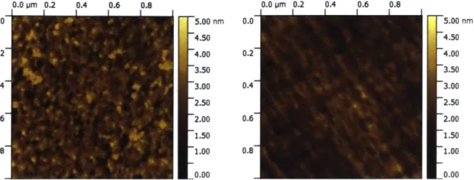
0.0 Imn 0.2 0.4 0.6 0.8 0.0 iu 0.2 0.4 0.6 0.8 0.0 Jim 0.2 0.4 0.6 0.8 0.0 5.00 rm 0.0 5.00 m D.0 5.00 ry 4.50 4.50 4.50 0.2 4.00 0.2 4.00 0.2 4.00 3.50 3.50 3.50 0.4 3.00 0.4 3.00 0.4 3.00 2.5 2.5D 2.50 0.6 2.00 0.6 2.00 0.6 2.00 1.50 1.50 1.50 0.8 1.00 0.8 1.00 0.8 1.00 0.00 1 0.00 0.00
a. RMS roughness=0.3nm b. RMS roughness=0.3nm c. RMS roughness=0.5nm Figure 2-1. lumxlum AFM scans for samples S1 (a), S3 (b), S5 (c). The rms roughness is low and all samples have features with peak-valley amplitude 1nm-3nm with spatial wavelengths of 10-30nm.
We note that surface hillocks are observed in optical differential interferometric contrast images like in Figure 2-2a on all samples in Table 2.1. By selectively etching the germanium layer using H202
without etching the underlying Si5oGe5o regrowth layer, the hillocks are not observed confirming that they are formed during the growth of the Ge layer. The hillocks density is (1-2) x106cm-, which is equal to threading dislocation density of Si5oGe5o buffers used in this study. To confirm the
correlation the hillocks with threading dislocations, we repeated sample S5 on a Si5oGeso buffer known to have a high defect density (threading dislocations visible in cross section TEM Figure 2-2d) and indeed it lead to a very high density of hillocks, ~1x1O8cm2 as seen in Figure 2-2b. The
hillocks can be formed due to enhanced growth rate near a pre-existing dislocation due to either spiral growth around of the Si5oGe5o substrates suggesting that these hillocks are spiral mounds growing at an enhanced growth rate due to the extra surface step due to the screw component of the dislocation.
a b ISGe5 Regrowth 2 0 0 n m la y e r d cd
Figure 2-2 Effect of initial dislocation density on hillock density for S5. The hillock density in (a) and the XTEM of the low pt SisoGeso regrowth layer are representative of all the samples studied. (b) shows a significantly higher density
(>108cm-2) when S5 recipe is repeated on a Si5
oGe
5o buffer created with a high dislocation density as shown in (d) After the furnace annealing the films remain planar, however there is an increase in roughness for S3(13nm). In contrast, ramping the temperature in situ to 5000 C leads to islanding of the 13nm film. We attribute this difference to the presence of a native oxide on the Ge surface when annealed in the furnace tube. The oxide desorption rate in the furnace tube is expected to be slow because forming gas flow rate used is low. Also, the furnace has a higher background oxygen content than the CVD reactor. After the growth of a thin low temperature layer, growth of a second Ge layer at
5000 C also lead to 3D island growth for samples with and without any ex-situ furnace anneal. As
will be discussed in the following section, the island formation is due to high residual strains of the low growth temperature layers. The strain relaxation and crystallographic defects are studied only for the films that do not undergo 3D island formation.
0.0 trm 0.2 0.4 0.6 0.8 0.0 0.21 0.4 0.6 0.8
a. S3 post anneal RMS roughness=0.7nm
5.00 nm 4.50 4.00 3.50 3.00 2.50 2.00 1.50 1.00 0.00 0.0 0.2 0.4 0.6 0.8 0.0 pm 0.2 0.4 1 1 1 0.6 0.8
b. S5 post anneal RMS roughness=0.5nm
0.0 om 0.2 0.0 1IIr 0.4 0.6 0.8 0.2 0.6 0.8 70 nm 60 40 30 20 10 0 0.0 pm 0.2 0.4 0.6 0.8 0.0 0.2 0.4 0.6 0.8 70 nm 60 50 40 30 20 10 0 c. S8 RMS roughness=11.8nm d. S9 RMS roughness=10.9nm
Figure 2-3 lumxlum AFM scans for samples for processing and growth at 500C. S3 (a), S5 (b) remain planar after ex situ annealing but S8 (c) and S9(d) show 3D island have formed.
2.3.2. Plastic relaxation
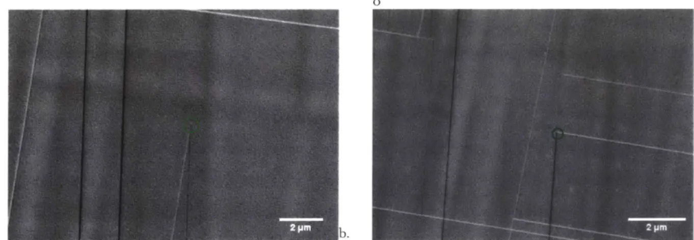
Low Growth Temperature Films -Because ECCI allows imaging of very large areas, strains as low as 10' can be measured with ease. The measured critical thickness for incoherency (h) islOnm.
5.00 nm 4.50 4.00 3.50 3.00 2.50 2.00 1.50 1.00 0.00
a. b. " Figure 2-4 ECCI imaging under a "3 beam condition" revealing misfit dislocations in the primary slip system at the Ge/Si5oGe5o interface for samples S3 (a) and S5(b).
As the film thickness (b) increases to 13nm for S3, we observe long misfit segments due to the glide of grown in threading dislocations shown in Figure 2-4a. There are no signs of dislocation
nucleation; the misfit segments ends are either connected to the surface hillocks or at an intersection with an orthogonal misfit dislocation and the line segment density is approximately equal to the hillock density unlike thicker samples (S5 shown in Figure 2-4b). Hence the strain relieved for this
sample should only be dictated by dislocation glide of the pre-existing dislocations. The strain relief
Ep ~4x10⁻⁵ measured for this sample corresponds to a glide velocity of 0.8umst. This velocity can be compared to dislocation velocity measurements in bulk crystals by appropriately accounting for the back stress (line tension, image force and lattice friction). Since measured the strain relaxation is small we can calculate the excess stress U-ex from the resolved stress due to an elastic strain - E
=2x10² scaled by a factor of (1-he/h) to account for the back stress, that gives Gc -265MPa for
h=13nm. Using the stress and temperature dependent dislocation velocities parameters [17] for undoped Ge, we would expect a glide velocity in the 0.2ums' - 3.5 ums-1 range for activation energies of 1.74eV -1.58eV consistent with our measurement.
As the thickness increases with samples S4 and S5, we see an increasing number of "Y-center" defects [18] shown in Figure 2-5a indicating that induced dislocation nucleation by complementary 600 dislocations is active. Similar to high Ge composition Sii-Gex/Si films grown at comparable growth temperatures, such films will have significant density of complementary pairs of 600
dislocations that react to form an edge dislocation [19]. Bolkhoityanov et al. have reviewed [20] how these dislocations effectively act as mobile edge dislocations. By counting the number of line
segments, we can estimate the number of threading dislocations. Our ECCI images were performed in a single "3-beam" condition and hence we cannot directly differentiate between pure edge and
600 dislocation segments without a g.b analysis at different g vectors. Therefore, we cannot calculate the exact amount of strain relieved, but we can obtain a lower bound by assuming that all the line segments are 60* MDs and an upper bound by assuming that all are 90' MDs. Similarly, for calculating the dislocation density, we obtain a lower bound on the dislocation density by assuming that only a single threading segments exists at the each terminal of the misfit segment and an upper bound for 2 threading segments associated with each misfit segment. As will be evident in Figure 2-8, since these measurements vary by orders of magnitudes in our samples, this error is acceptable for all the following discussions.
In addition, we note that we see a change in contrast for some intersections of dislocations travelling in orthogonal directions, like the one in Figure 2-5b confirming that edge dislocations formation by cross slip [21] is also operative.
a. b.
Figure 2-5 ECCI images of sample S4. (a) shows a "y-center" defect and (b) shows a change in contrast at in intersection of orthogonal dislocations indicating that edge dislocations are formed by cross slip.
For samples S6 and S7 as the strain relaxation increases, we cannot resolve individual MDs in ECCI and hence the residual strain is measured using XRD. Figure 2-6 show reciprocal space maps of (004) Bragg peaks for samples S6 and S7 used to calculate the out of plane lattice constant of Ge from which its residual strain is calculated as 1.6x1 02 and 1.0x10²
respectively. Compared to thin samples (S1-S5), S6 and S7 have higher strain relaxation (> 1x10³).
-A 3.5 3A5 2 7.5 3 7.1-a.. 3.5 F 4s 2 1.5 7.0 .5 5.1 a. b.
Figure 2-6 004 Reciprocal space maps of S6 and S7 used to measure the residual strain in the Ge film.
Cross section TEM shows that planar defects haven been nucleated. Since planar defects are more commonly associated with tensile strained films than compressive strained films [22] (for growth (001) interfaces), some discussion is warranted. Typical stress related causes of planar defects are i) nucleation of a half loop with a single partial dislocation creating a stacking fault (ii) increase in dissociation width of an existing 600 dislocation composed of 900 and 300 partial creating a stacking fault or (iii) creation of microtwin defects. For compressively strained films, if a 900 partial of a misfit dislocation is nucleated first, the stacking fault thus created is an unfavorable high energy stacking fault [23], [24] and hence a complete 600 misfit dislocation [22] has to be formed ruling out (i). As pointed out by Nijenhuis et.al [25] , the extension of this criterion has been incorrectly
extended [23] to 600 threading dislocations since the leading/lagging partials in the threading arm are the opposite to that of the corresponding misfit dislocation. Therefore, for threading dislocations, mechanism (ii) is favorable. Microtwins have been reported for high misfit compressively strained films [26], [27] during growth and in Si1aGex films formed by the Ge condensation technique used to produce Silicon-Germanium on oxide wafers [28], [29] and are likely present in these films.
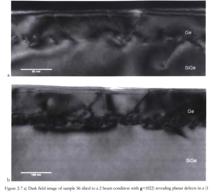
a
b
Figure 2-7 a) Dark field image of sample S6 tilted to a 2 beam condition with g= (022) revealing planar defects in a (111) plane.
b) Bright field image of sample S7 tilted to a 2 beam condition with g=(022) revealing planar defects in a (111) plane.
The fringes near the surface are due to the high tilt deviation from the (110) zone axis
Figure 2-8 shows the strain relaxation (a) and defect densities (b) of Ge films of different thicknesses as measured by the methods described above. The equilibrium strain-thickness curve plotted in Figure 2-8a is calculated by balancing the force on a dislocation due to the misfit stress with the line tension force for 600 dislocations in the primary slip system - < 110 > {111} for a cubic
anisotropic crystal. The low temperature Ge layers on SisoGe5o remain highly strained in contrast to the low temperature Ge growth on Si [30] that undergoes island growth and coalescence. This metastability is discussed further in the next section in context with the annealing of these films to
again is different from the Ge on Si growths [7], [30] where threading dislocations with a density greater than 1010cm-2 are nucleated in the initial stages but they reduce by annihilation/fusion reactions to ~109cm2 for
-1um
thick films.2.5E-2 --- Calculated equilbrium 1E+10
state X Low temperature
growth
2.0E-2 -~ X X X + Ex-Situ annealed 1E+9
1.SE-2 I 1E+8 Residual udefe Strain I + density 1.OE-2 % cm 2 1E+7 %S % 5.0E-3 1E+6 0.0E+0 1E+5 0 20 40 60 80 100 0 20 40 60 80 100 Thickness (nm) Thickness (nm) a b
Figure 2-8 a) Residual film measured for the as grown sample and after ex-situ annealing. For residual strains < 1.8x10⁻², XRD was used and for higher residual strains ECCI used to calculate the misfit length. (b) shows how the defect density increases with thickness. For the S6 and S7 (thicknesses 46nm and 97nm), an order of magnitude estimate is made on the basis of their detection in X-TEM.
Ex-situ Anneal- Since all the as grown (3800 C growth temperature) samples are highly strained, we annealed the samples in a tube furnace at 5000 C for 1 hour with forming gas to create more
strain relaxation. The annealing conditions should result strain relation > 102 by glide of mobile
unimpeded dislocation density of 106cm-2.
a. b.
Figure 2-9 ECCI imaging under a "3 beam condition" revealing misfit dislocations in the primary as well as secondary slip system at the Ge/SisoGeso interface for samples S3 (a) and S4(b) after furnace annealing.
ECCI images of thin annealed samples shown in Figure 2-9 show MDs in the <110> directions, but in addition reveal dislocation segments that run approximately along <100> directions. This was observed in high compressively strained InP films on relaxed InGaAs and it was demonstrated that a 600 MD initially in the < 110 > {111} primary slip system cross slips onto the a < 110 >
2 2
{110}
secondary slip system [31]. The line direction of these segments is changes frequently and is explained by a frequent cross slip between the two slip systems. The mechanism for motion of such segments could be climb [32] which is supported by the absence of this mechanism during the lower growth temperatures. However, we cannot rule out glide as well [31].Figure 2-8a shows that although additional relaxation occurs during annealing, the films still remain highly metastable. Long range [33] and short range blocking [34] due to interactions of a single orthogonal MD have only a marginally higher residual strain than the calculated equilibrium curve. Hull et. al [35] have discussed that in the initial stages of relaxation image forces and blocking by
orthogonal MDs can be a stronger effect for high lattice mismatch films than low lattice mismatch films. This is because the critical thickness is lower for high mismatch films when image forces contribute significantly. However that cannot explain why thicker films (S5-S7) do not relax further. We suspect that a stronger pinning effect of the mobile threading dislocations is prevalent in our thicker films either due to planar defects [36] formed under high residual stress or due to blocking effects of a dense array of MDs being stronger than that of the individual MDs usually employed to study such blocking phenomenon.
a b
Figure 2-10 X-TEM of samples S4 (a) and S5(b) after furnace annealing.
2.4. Conclusion
Eresidual%2*
I
.Ic
I
b
....
106
107
108
109
1010
Defect Density
cm-
2Figure 2-11 Processing paths for producing strain relaxed Ge films on Si substrates. I- graded buffer.;II- low temperature (H1a) -high temperature (1Ib) growth on Si followed by cyclic annealing (lIc); III growth on relaxed SisoGeso buffer layer in this work
Ge films are grown on Si5oGeso buffers in a 2D planar growth mode. Glide of pre-existing
dislocations provide only limited strain relaxation and Ge remains highly strained compared to what is expected from blocking effects of isolated misfit dislocations. The results indicate that achieving low defect density relaxed Ge films on Si5oGe5o is more difficult than on Si substrates. This is not intuitive a priori since the former has a lower lattice mismatch and a larger process window for strain and defect management would be expected. Figure 2-11 shows a schematic of 3 different processing paths to achieve strain relaxed Ge on Si substrates that have different residual strains and defect density during growth. Path I represents graded buffers as in references [8] [37], that have the lowest defect densities and residual strains during growth. Path II represents the Ge/Si process [7] that undergoes island growth and coalescence (Ia) during which a high density of misfit dislocations are formed relaxing most of the strain and producing a high threading dislocation density and avoiding planar defects. The threading dislocation density is then decreased by dislocation
interactions in the absence of high residual strain by growing a thick uniform layer (fIb) followed by thermal cyclic annealing (I1c). In the system studied here, Path III, the films remain highly strained as there was no kinetic pathway for the mobile dislocations to relax strain by their glide, allowing a high density of threading dislocations/planar defects to nucleate. This stability of a highly strained state can be beneficial for Ge channel MOSFETs in reference [38] but not for obtaining strain
relaxed Ge layers. Although the defect densities of the low temperature growth layers are lower than comparable Ge/Si seed layers planar defects are nucleated due to the high residual strain. Future studies are required to determine if growing thicker strained relaxed films with cyclic thermal anneals can reduce the dislocation density lower than comparable Ge/Si processes.
Chapter 3
Dislocation dynamics in low misfit
Inx(AlyGa1-y)1-xAs films grown on relaxed Ge buffer
layers on silicon substrates
3.1. Introduction
The ternary alloy system Inx(AlyGa,_y)1-As finds applications in optoelectronic devices like light emitting diodes, solar cells and photodetectors with a direct bandgap in the near IR range of wavelengths. These alloy systems are also utilized in high frequency devices like HEMTs due to a high carrier mobility. One promising path towards heterointegration of this alloy with Si CMOS involves epitaxial growth of this alloy system with the use of an intermediate Ge buffer layer on a miscut Si substrate that accommodates most of the lattice mismatch between Inx(AlyGa,_y)-xAs and Si without introducing deleterious anti phase defects.
In this chapter we consider the dislocation defect structure involved in the growth of low indium Inx(Al25Ga7 5)1_xAs films on relaxed Ge buffers. During their growth, these films inherit the threading
dislocations already present in the Ge buffer layer. The smaller lattice mismatch between the Inx(Al25Ga75)1_xAs and Ge that we introduce in our experiments cause these dislocations to move in order to relive stress and we aim to study the effect of this motion on the final defect density. Cathodoluminesce (CL) and ECCI imaging in an SEM is employed to study large areas of the
sample to quantify the defect densities. These experiments have a twofold purpose. First, the field of III-V on silicon is approaching commercialization and the effect of small lattice mismatch in device structures is important now. Second, the motion of these defects may be used to reduce their density as we discuss later in the chapter.
This Chapter is divided into 5 sections. First, the sample structures, their growth procedure, major characterization methods and some general aspects of strain relaxation are described. In the next section, we describe a recombination enhanced dislocation glide effect observed during the CL
density in In,(Al25Ga7s)1..As changes relative to the dislocation density of the Ge buffer layer. Finally, this is followed by a brief study on the effect of growth area on threading dislocation density, i.e. effect of growing an In.(A25Ga7s)1.,As structure on mesas different sizes.
3.2. Experimental details
150mm Silicon substrates with their surface normal offset from [001] by 6 0 towards the nearest
[111] direction were used to discourage APD formation [4]. The epitaxy on these substrates were prepared by a multi-step growth procedure. Germanium is first grown on 150mm Silicon wafers in an Epi Centura LPCVD reactor by a two temperature step procedure following the procedure in references [7], [13]. 150nm of GaAs is then grown on these wafers in a Thomas Swan/Aixtron MOCVD reactor with a high AsH3 over pressure [5] to suppress APD formation. These wafers are cleaved into smaller pieces and treated as "pre-threaded" substrates for subsequent Inx(AlyGay) 1_As growth in the MOCVD.
Pre-threaded substrates with two different dislocation densities are prepared. For a moderate
dislocation density (M), the germanium layer is grown 1.2um thick and 5 cycles of thermal annealing (6500C-8500C) are performed. For a high dislocation density (H), the germanium thickness is 0.3um and no high temperature cyclic annealing is performed.
The precursors used for the Inx(AlyGa,_y)iAs films are trimethylgallium, trimethylindium,
trimethylaluminum and arsine. The carrier gas is H2 and the films are doped n type ~1E17 using
disilane. The films are grown at 7250C with a V/III ratio of -40 and growth rates varying from 1-1.4nm/sec. A -200nm GaAs layer of homoepitaxy is grown on all samples before any the Inx(AyGa,_y) 1-As is grown to minimize any effect of contamination at the regrowth interface. By growing Inx(AlyGa,_y)1 As on these "pre threaded" substrates we avoid the issue of the initial nucleation of dislocations in low/dislocation-free substrates[39].
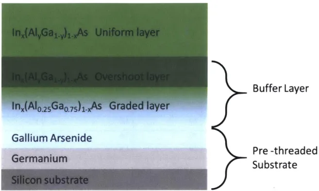
ln,(AlyGaj.y)
1-As
Uniform layer
lnx(Al
0.2
5Ga
0.7
5)
1-xAs
Graded layer
Gallium Arsenide
Germanium
Silicon substrate
Buffer Layer
Pre -threaded
Substrate
Figure 3-1 Schematic of the different layers of the samples studied in this chapter.
Figure 3-1 is a schematic of the samples used in the study and they are detailed in Table. Most of the uniform layers of the samples mostly, an aluminum fraction of 0.25.
Cathodoluminescence samples have a ~100nm layer of Al fraction of 0.15 sandwiched between higher bandgap clads to incorporate a double heterostructure without changing the lattice constant. This allows a high radiative efficiency in an active layer away from the lattice mismatch interface and hence a small dark spot radius of threading dislocations in cathodoluminesce, allowing for a higher resolution of the defects than in unclad films.
Table 3.1 Details of the layers that together constitute the In.(Al25Gays)1.As epistack
%In Grade Rate Uniform layer thickness Overshoot
(I0 n/um) (urn) layer
M1 0 - 1.6 N M2 2 - 1.6 N M3 5 - 1.6 N M4 5 - 1.6 Y M5 5 10 1.6 Y M6 5 5 1.6 Y
M8 3 10 1 Y M9 5 10 1 Y M10 9 10 1 Y G1 5 - 1.6 N H1 10 - 0.12 N H2 10 - 0.24 N H3 10 - 0.39 N H4 10 - 0.6 N H5 5 10 1.6 Y H6 10 10 1.6 Y H7 15 10 1.6 Y
One sample is grown on GaAs, G1 to control for CTE related concerns. Unfortunately, it is an imperfect control since the dislocation density is significantly lower (by a factor~2x10⁴) than that of the films grown on Ge/Si. Preliminary efforts to use a sequence of compressive followed by tensile InxGai-,As graded layers to create a GaAs template with comparable threading dislocation density with Ge/Si failed to produce a dislocation density higher than 106cm-2.
CL imaging
The presence of Al in Inx(AlyGai-y)1._As allows us to keep the bandgap emission wavelength <
800nm within the responsivity range of the available detector for all samples. The accelerating voltage used for imaging is 5kV. This corresponds to a penetration depth of ~300nm for the
primary generated electron-hole pairs. The top clad thickness used in all the samples is ~400nm and hence the primary carriers are contained in the top cladding layer region as shown in the schematic
I 110 ,
Top Clad TD; d 1ol
te ,. . 110 L1 MD e TD ta Active Layer I \ IL2 Loo -Bottom Clad L3
I
tc L4 Buffer LayerFigure 3-2 Schematic depicting the interpretation of defects at different depths from the surface for cathodoluminesce maps
These carriers may combine radiatively or non-radiatively within the top cladding layer or they may diffuse to either the free surface or the active layer. Surface recombination velocity is very high for an unpassivated surface and is the dominant recombination mechanism and the top cladding layer will have a low effective carrier lifetime and hence low diffusion length. The active layer has a lower bandgap than the cladding layers by ~0.1eV. Band bending near the active layer/clad interface facilitates transport into the active layer, increasing its excess carrier concentration and its radiative efficiency. The 0.1eV confinement -4kT is not sufficient to confine all the carriers in the active layer and some carriers will escape into the bottom clad layer.
We now consider how dislocation defects in these layers can contribute to contrast in CL images with aid of the schematic in Figure 3-2. The interpretation of the defect signatures in CL is
confirmed in the third section but is discussed here to interpret some inferences from CL in the second section. Dislocations are centers of non-radiative recombination. CL signal diminishes near a distance L around the dislocation, where L is the diffusion length of the excess carriers. The
contrast due to a dislocation depends on how strong the recombination at dislocations is compared to all other recombination paths. Thus dislocation contrast in CL can be discussed in terms of the
size of the dark region and its contrast. Threading dislocations (TD) create a dark spot. A misfit (like) dislocation MD, shown in Figure 3-2 in the top cladding layer (d<tic), where the surface recombination decreases the carrier lifetime significantly, produces a low contrast, thin dark line like L1. For dislocations in the active layer (ttc<d<tc+tc), the contrast and the dark spot line width are be
dislocations is very faint. If a dislocation lies in both the top cladding and active layer, as in the case of a dislocation half loops its dark line width will vary as depicted by L4. Contrast due to
dislocations at the interface require a more detailed numerical analysis. On a relative basis, interface dislocations between the top cladding and active layer will have a thinner CL signature compared to that between the active and bottom cladding layers. There is a high density of misfit dislocations at the interface between the bottom cladding layer and the active layer. These however, cannot be resolved because
-i) The spacing between these misfits is too low to be resolved in the bottom cladding layer where the diffusion length is very high and the CL resolution is poor.
ii) The carrier concentration in the bottom cladding layer is very low and hence radiative recombination in this layer has a minor contribution to the total pan-Cl signal.
Carriers may combine radiatively in the-bottom clad but its radiative efficiency is lower than the active layer due to a low concentration of excess carriers. The intensity of the signal measured in the range of active layer wavelengths is >4x the intensity of the signal measured from the cladding layers. However, most imaging performed in this study was performed using a pan-CL detector that is not wavelength resolved and has a higher responsivity for cladding layer wavelengths than active layer wavelengths. Hence effectively, comparable signal from both the (top) cladding and the active layer contribute to such images. Any emission from the defect itself is at longer wavelengths and cannot be detected by the detector used. Thus, the CL experiments have been designed to produce signal only from the top part of the structure where ideally, only threading dislocations are present. All CL imaging was performed by Eamonn Hughes and Connor Reilly in Prof. Kunal Mukerjee's research group at UCSB.
Strain Relaxation
At a growth temperature of 7250C, In1 (A25Ga75)99As is lattice matched to the lattice constant of bulk relaxed Ge. The actual in-plane lattice constant of the Ge film on silicon will be smaller than its natural relaxed value due to residual compressive strain in the film. The equilibrium residual strain calculated by applying Mathews force balance criterion for an anisotropic cubic crystals relaxing only by plastic deformation by the primary slip system predicts a small residual strain of -1.7x10⁴ for the Ge film (negative strain corresponding to in-plane compressive strain). The actual residual strain is expected to be higher due to kinetic [40] and work hardening [41] effects but we can expect it to be
in the same order of magnitude. For the In,(AlyGa,_y)1 As films studied in this chapter, the strain is compressive during growth. The films are grown sufficiently thick and several employ graded buffers that lead to a high degree of relaxation during growth and hence a low residual compressive strain Er,Tg after the growth concludes at the growth temperature Tg. As the sample cools down to room temperature, the residual strain in the films change because of differences in the coefficient of thermal expansion (CTE) of the substrate and the films. All the In.(AlyGai-y)iAs films studied here and Ge have a closely matched CTE but the silicon substrate has a significantly lower CTE .If no relaxation takes place during cooldown, this strain in the Ge and Inx(AlyGa,_y)iAs shifts in the tensile direction by EcTE-2x10 3. Any relaxation due to the accumulation of tensile strain during cooldown, 6cCO.1 is considered to be a smaller effect since the velocities of the dislocations will
reduce drastically with decrease in temperature and the temperatures can drop from 7250C to
~4000C in a short duration of 5mins after which no significant dislocation relaxation is expected. The measured residual strain (Er:: Er,Tg+ ECTE+ 86coo,) reported here is the net result of all the three
effects. All the measured films have a residual tensile strain Er ~(1-2)x10 3.
3.3. Recombination Enhanced Dislocation Glide (REDG)
At room temperature, in most semiconductors dislocations cannot overcome the Peierls barrier and are immobile. When the tensile strained Inx(AlyGai-y)v As films are imaged using CL, kinetic barriers for motion may be lowered due to recombination of carriers generated by the electron beam, allowing dislocations to glide. This effect, termed recombination enhanced glide and has been studied comprehensively for GaAs by Maeda and Takeuchi [42] by applying strain using a mechanical bending apparatus inside an SEM and tracking dislocation motion using CL. They performed quantitative velocity measurements for n doped bulk GaAs specimens by activating only a single slip system; type o, P and screw of <110> type line segments had significantly different velocities shown in Figure 3-3 .At room temperature, x type dislocations have the fastest velocities,
relative to which screw dislocations are expected to have lower velocities by a factor of 10' and P 600 a factor of 10-6 compared to the (x 600 dislocations. They reported activation energies for (X,

![Figure 1-2 Sensitivity of GaAs solar cell performance to threading dislocation density from reference [11].](https://thumb-eu.123doks.com/thumbv2/123doknet/14751068.580198/18.917.113.654.202.527/figure-sensitivity-gaas-performance-threading-dislocation-density-reference.webp)