An Automated Method for Data Path Construction
by
Darren A. Schmidt
Submitted to the Department of Electrical Engineering
and Computer Science in Partial Fulfillment of the Requirements
for the Degrees of Master of Engineering and Bachelor of Science
in Electrical Engineering and Computer Science at the
Massachusetts Institute of Technology
May
1998
Copyright 1998 Darren A. Schmidt. All rights reserved.
The author hereby grants to M.I.T. permission to reproduce and
distribute publicly paper and electronic copies of this thesis
and to grant others the right to do so.
Author
Department of Eectrical Engineering and Computer Science
May 20, 1998
Certified
by-SChris
Terman
:
Thesis Supervisor
Accepted by
Arthur C. Smith
Chairman, Department Committee on Graduate Theses
An Automated Method for Data Path Construction
by
Darren A. Schmidt
Submitted to the Department of Electrical Engineering
and Computer Science in Partial Fulfillment of the Requirements
for the Degrees of Master of Engineering and Bachelor of Science
in Electrical Engineering and Computer Science
at the Massachusetts Institute of Technology
Abstract
The construction of custom data paths is a time-consuming and difficult problem.
Even with a library of standard cells, custom hand layout can take months. In addition,
minor design changes or revisions for next generation designs can be tedious and
difficult. By creating an automated system, data path design can be greatly simplified
and dramatically sped up. Not only does this aid in the initial design, but it also enhances
the designers ability to make design changes.
Now these revisions involve simply
modifying lines of code, rather than the painful process of redoing a custom layout. In
addition, changes to new technology are easily accommodated. Rather than redo the
entire design, only the standard cells and the affected constants in the program need to be
revised. Then, the program can be rerun and a new design can be created. One of the
drawbacks of automation is that it reduces the designer's flexibility in layout.
In
addition, many existing tools are complex and difficult to use. The goal of this project is
to create an easy-to-use, automated design tool that results in all of the benefits
previously mentioned, while at the same time giving the user maximum flexibility in
design. This thesis describes the implementation of such a system, as well as the results
of using this tool to create a substantial design.
Thesis Supervisor: Chris Terman
Title: Professor
Acknowledgements
There are many people without whom this thesis would not have been possible and to
them I give my thanks:
To Professor Gerry Sussman and Amorphous Computing, for giving me the
opportunity to work in their group.
To Professor Chris Terman, for not only being a great thesis advisor, but also a
great teacher and friend.
To my family, for providing me with their continued love and support.
To my roommates and friends, for helping me to enjoy my MIT experience.
Contents
1 Introduction
7
1.1
Background ... 7
1.2
Objectives ...
...
... 9
1.3
Amorphous Computing ... ... 10
1.4
Thesis Outline ... ...
12
2
The Building Blocks: Standard Cells
13
2.1
System Overview ...
13
2.2
A Basic Standard Cell ...
... 14
2.3
Standard Cell Layout ...
... 16
2.3.1 Facilitating Tiling ...
...
16
2.3.2 Simplifying Routing ... ... 16
2.4
Standard Cell Library ...
... 17
2.4.1
Basic Gates ...
... 17
2.4.2 XOR and XNOR ...
..
... 18
2.4.3 Registers ...
...
19
2.4 .3 M ultiplexor ...
19
3
The Place and Route Tool
22
3.1
Program M ethodology ... ... 22
3.2
Performing Placement ...
...
23
3.3
Performing Wiring ...
24
3.3.1 Routing Signals ...
... 25
3.3.2 Routing Power and Ground ...
... 27
4
Data Path Elements
30
4.1
32-Bit A dder Design ...
... 30
4.1.1 Binary Full Adder ...
...
31
4.1.2 Ripple-Carry Adder ...
31
4.1.3 Carry-Skip Adder ...
... 32
4.1.4 Manchester Adder ...
...
33
4.1.5 Binary Lookahead Carry Adder ...
36
4.1.6 Final Results ...
42
4.3
A dditional B locks ...
... 43
5
Taking the Tool for a Test Drive
45
5.1
A 32-B it C ounter ...
45
5.2
Building the C ounter ... 46
5.2.1
32-Bit Multiplexor ... 47
5.2.2 32-Bit Register ...
... ... 47
5.2.3 C ounter Logic ...
...
48
5.2.4 Putting It All Together ...
...
48
5.3
Possible Im provem ents ... 52
5.3.1 Improving W iring ... 52
5.3.2 Enhancing the Routing of Power and Ground ... 53
5.3.3 Accepting Additional Input Styles ... 54
6
Conclusion
55
Appendices
56
A . 1 m agic.scm ...
...
.. ...
56
A .2
counter.scm ... ...
86
List of Figures
2-1
Basic Routing Plan ...
.... ... 14
2-2
Basic Gate Layout ... ...
15
2-3
XNOR Schematic and Layout ...
... 18
2-4
2:1 Multiplexor Schematic and Layout ...
19
2-5
Jam Register Schematic and Layout ...
20
4-1
Full Adder Schematic ... ....
... 31
4-2
Manchester Carry Adder Schematic ...
33
4-3
Conflict-Free Manchester Carry-Skip Circuitry ... 34
4-4
32-Bit Manchester Carry-Skip Adder Schematic ... 35
4-5
Binary Look-Ahead Carry Adder Block Diagram ... 37
4-6
GP Block Schematic ... ...
... 38
4-7
BA and BB Block Schematics ...
... 38
4-8
4-Bit BLCA Adder Schematic ...
...
40
4-9
32-Bit BLCA Adder Schematic ...
....
41
4-10
32-Bit BLCA Adder Layout ...
... 44
5-1
32-Bit Counter Schematic ...
46
Chapter 1
Introduction
This thesis describes the implementation and test drive of a standard cell layout
tool for data paths. This chapter begins with a summary of previous work in the area of
automated placement and routing tools and a description of the goals of this project. It
then provides an introduction to the larger project for which this work is being done and
concludes with an outline of this thesis.
1.1 Background
The automated conversion of a VLSI design to layout has been an active area of
research for the last 15 to 20 years. This task entails three main phases, cell design,
placement and routing. A number of algorithms have been developed to solve the last
two of these problems.
There have been two main approaches to the problem of placement, the task of
placing modules adjacent to each other in order to minimize area or cycle time. The
Min-cut algorithm' performs placement by partitioning. It divides the blocks to be placed at
the top level of the design into two groups of approximately equal area, while minimizing
the number of connections required across this divide. This process is then repeated for
the two halves, splitting the layout into quarters, eighths, and so on, until the leaf cells are
reached. Another widely used technique is one in which the movement of modules is
likened to thermal annealing.
2Modules are initially moved randomly, and the
or timing. As the layout "cools", the routing and/or timing improves. For each proposed
subblock movement, the resulting temperature is calculated. If it is higher than the
current temperature, the move is not completed. To avoid local minima, the "melt" is
reheated and then recooled according to an "annealing schedule".
The lowest
temperature configuration found so far is saved before each movement, and the algorithm
stops when after a given number of tries a new minimum is not found. Both of these
methods have been widely used, although they require significant runtime.
A variety of routing tools have been developed as well. Routing is the task of
taking a module placement and a list of connections and connecting the modules with
wires. One common type of router is a channel router, which routes rectangular channels.
The greedy channel router
3wires up the channel in a left-to-right, column-by-column
manner. Within each column the router tries to maximize the utility of the wiring
produced, using simple "greedy" heuristics. Global routers
4are channel routers that
attempt to minimize the total number of wiring tracks required by examining the entire
design and generating all possible net segments for each net. Then, it chooses from
among all possible net connections in order to minimize the total channel density. There
are also more complicated routers, such as maze routers. These can route just about any
configuration, but have comparatively long running times. They are usually reserved for
very difficult routing problems. These routing methods have also been widely used, and
there are many custom routing tools as well.
There currently exist a number of tools that perform both routing and placement
for standard cell designs. One such tool that is in wide use is TimberWolf.
5This tool
the routing. This package provides good results and substantial area savings, compared
to other standard cell layout methods.
The above mentioned placement and routing tools provide reasonable solutions to
the general VLSI design problem. However, they fall short in a few areas when it comes
to data path design. The current automated systems minimize the role of the designer. In
addition, they don't group standard cells by function, but rather to optimize area or
timing. Thus, it can be difficult to understand the resulting layout. Finally, they are
complicated to use and often require considerable amounts of run-time.
1.2 Objectives
The goal of this project is to create a tool that provides the best of both worlds.
That is, it should provide the benefits of automation and reduce design time. But, it
should do this while still giving the designer complete control over the layout. It should
also result in a logical grouping of standard cells, so that designs can be easily followed
and debugged. Finally, it should be easy to use and relatively fast. Since the designs of
data paths and their resulting layouts tend to be regular, placement and routing are often
quite straightforward from the designer's point of view. Thus, a designer-directed layout
strategy should perform very well without too much effort on the part of the designer. In
addition, this strategy would result in a logical placement of standard cells that could be
easily followed by the designer. And unlike many of the more complicated algorithms, it
would be relatively easy to use and have a very short run-time.
This thesis attempts to illustrate the usefulness of an automated system of the type
previously described. First, a prototype of such a system will be created. This will
involve the layout of the standard cells that are necessary for data path construction, as
well as implementing a method for building with these cells.
This method of
construction will be created in the form of a Lisp program. Finally, a sample data path
will be constructed using this prototypical tool.
While by no means the optimal
implementation, this project is instead intended to prove the usefulness of such a tool.
Once the basic tool is built and tested, it can then be refined and the user-interface can be
improved upon at a later date.
1.3 The Amorphous Computing Project
One of the major current activities of the Mathematics and Computation Group of
the Artificial Intelligence Lab is the study of amorphous computing. Drawing from
natural phenomenon such as a swarm of bees cooperating to construct a hive, this group
is attempting to address the fundamental organization of computer systems.
Two
fundamental questions they have raised are:
1) How do we obtain coherent behavior from the cooperation of large numbers of
unreliable parts that are interconnected in unknown, irregular, and time-varying ways?
2) What are the methods for instructing myriads of programmable entities to cooperate to
achieve particular goals?
The objective of this research is to create the system-architectural, algorithmic,
and technological foundations for exploiting programmable materials.
These
"programmable materials" are materials that incorporate vast numbers of programmable
elements that react to each other and the environment. In order to do this, the group is
attempting to identify engineering principles for organizing and instructing a myriad of
programmable entities to cooperate to achieve pre-established goals, even though the
individual entities are connected in unknown, irregular, and time-varying ways.
Amorphous computing is inspired by the recent developments in molecular
biology and in microfabrication. Each of these is the basis of a kernel technology that
makes it possible to build or grow huge numbers of almost-identical
information-processing units, with integral actuators and sensors, at almost no cost. Microelectronic
components are so inexpensive that the group can imagine mixing them into materials
that are produced in bulk, such as paints, gels, and concrete. Such "smart materials" will
be used in structural elements and in surface coatings, such as skins or paints.
6The role that the work of this thesis will play is to help create the second and third
generation of the amorphous computing hardware. The group hopes to incorporate all of
the necessary hardware for each individual element onto a single chip. This includes the
processor, memory, and a radio for communications. The tool developed and used for
this thesis will be used to create the processor portion of this chip. For the second
generation of hardware, an existing processor design will be created in our new design
environment. This will then be combined with memory and the radio, and put onto a
single chip.
It is hoped that this tool will eventually be used to implement a
microprocessor similar to the Hitachi SH-3, which the group is currently developing.
This enhanced processor would then be used for the third-generation of amorphous
computing hardware.
1.4 Thesis Outline
This chapter has presented a summary of past research in automated layout tools,
as well as an overview of this project.
Chapter 2 delves into the first part of this project, the creation of a library of
standard cells.
Chapter 3 then turns to the implementation of the layout tool that is used to put
these standard cells together to create circuits.
Chapter 4 focuses on using this tool to create larger data path elements.
Chapter
5
then describes the use of this tool to create a substantial data path
design and assesses the performance of this tool in performing this task.
Finally, Chapter 6 concludes this thesis with the author's comments on this
experience.
Chapter 2
The Building Blocks: Standard Cells
The first part of this thesis involved the creation of a standard cell library. This
chapter details the design of the standard cells, which form the building blocks for data
path construction. These are the only parts of any given design that are laid out by hand,
which was done using the Magic layout editor
7. The first section of this chapter gives a
brief overview of the new design tool, which will aid in the understanding of the standard
cell design. The second section details the common set of design rules to which all
standard cells adhere.
The third section details how the design of the standard cells
facilitates placement and routing, while the fourth section describes the components that
are included in the library.
2.1 System Overview
In order to understand the standard cells, it is useful to have a general knowledge
of the system in which they will be used. The designer will write a program that utilizes
this tool to generate their design. Within this program, they will specify the layout by
tiling and copying existing standard cells in a specific fashion. Thus, all placement will
be completely controlled by the designer. The designer will then connect these standard
cells by specifying which nodes they wish to connect, as well as the channel(s) in which
this connection should be made. The process currently being used has four independent
routing layers: one poly and three metal. The poly and metall layers are reserved for
in-cell routing. Thus, the general inter-in-cell routing method used will be to divide the design
into a large grid of horizontal and vertical channels. Top-level routing will be done on
this two-dimensional grid, with metal2 runs in the vertical direction and metal3 runs in
the horizontal direction. Vertical metal2 runs will begin and end each wire by connecting
to the desired node within a standard cell. They will then be connected by a horizontal
metal3 run, in the horizontal channel specified by the user. In this way, the designer will
specify both the placement and the routing of their design. An example of the routing
scheme can be seen in Figure 2-1.
Figure 2-1: Basic Routing Plan
2.2 A Basic Standard Cell
A basic standard cell is illustrated in Figure 2-2. This 2-input NAND gate
demonstrates some of the main properties of all standard cells. Each standard cell
includes power and ground rails, which border the remaining circuitry. A row of PFET's
lines the top of the cell, while a row of NFET's complements it at the bottom. In
between, the appropriate connections are made via poly or metal 1. Nodes that need to be
accessed in the next level up in a design are connected to metal2 contacts centered at the
intersection of a horizontal and a vertical channel, to allow for over-the-cell routing.
Transistors were sized with the following points in mind. For most data path
circuitry, transistors can be fairly small. As a result, many transistors are minimum size.
Since PFET's are weaker than NFET's, they are generally twice as wide as the
corresponding NFET. Gates were also designed to match the speed of a minimum sized
inverter. For example, if two transistors are in parallel, then their width is doubled, as
can be seen in the NAND gate. In most cases, this is the most that was done to optimize
transistor sizes.
This particular processor design is most concerned with functionality, so most
standard cell circuitry is kept simple and reliable. Most standard cells consist mainly of
complementary logic and transmission gates. There are no dynamic logic gates, so that
recharging is not an issue.
2.3 Standard Cell Layout
The standard cells were laid out in a way to facilitate two main functions. First,
features have been incorporated to facilitate the tiling of multiple standard cells. Second,
they were laid out in such a way as to ease the routing of wires between standard cells.
2.3.1 Facilitating Tiling
The main concern in the tiling of standard cells is the connection of power and
ground rails. This problem is addressed by incorporating a few features into the standard
cells. First, all standard cells have a common height. In addition, each has an identical
set of power and ground rails, as described in the previous section. The width of these
rails is half the minimum width, or 4 lambda. This is so that when cells are stacked
together vertically, a minimum width power line will be created. The layout tool has
features that place the power/ground contacts as well as the ability to space out stacked
cells if necessary. Finally, these power and ground rails extend two lambda past their
standard cell circuitry, so that when two cells are placed next to each other the rails make
a connection, with no design rule errors.
2.3.2 Simplifying the Routing
The most important aspect considered in coming up with a set of standard cell
design rules was how to make routing as simple as possible. In order to prevent conflicts
with wires running between cells, the standard cells do not contain any metal2 or metal3
wires. In addition, to make it easy for the program to connect wires, all of the metal2
contacts are placed in the center of an intersection of a vertical and a horizontal channel.
Finally, the height and width of all standard cells are multiples of the horizontal channel
height and vertical channel width, respectively. This is so that when multiple cells are
tiled together either vertically or horizontally, each cell remains "on grid" and the
contacts remain at a channel intersection, as described above. For our particular process,
the minimum width of contacted metal2 wires is 4, while the minimum width of
contacted metal3 wires is 6. In addition, the minimum spacing between metal2 or metal3
wires is 4. Thus, these standard cells were designed around vertical channels with a
width of 8 lambda and horizontal channels with a height of 10 lambda. Note that in order
to make the 8 lambda vertical channels work error-free,
m2/m3
contacts in the same
horizontal channel and adjacent vertical channels must be offset to the left or right by
one. This offsetting is specified by the user, when necessary.
2.4 Standard Cell Library
The library of standard cells includes all leaf nodes that are necessary for the
construction of a processor data path.
This includes basic complementary gates,
registers, and muxes. As mentioned previously, no dynamic logic is used and most gates
are kept simple in order to insure functionality. It is hoped that this library can also be
used to implement other data paths as well.
2.4.1 Basic Gates
A considerable portion of the library consists of simple, complementary gates.
This includes inverters, NAND, NOR, AND, OR, and-or-invert, or-and-invert, and buffer
gates. Most of these are made up of minimum-width transistors, although there are also
larger versions. These gates with larger FET's are used mainly in places where large
drive is necessary.
2.4.2 XOR and XNOR
Rather than one of the smaller, exotic XNOR circuits that are widely known, a
more reliable, slightly larger design was chosen. The XNOR circuit used can be seen in
Figure 2-3. The feature that makes it attractive is that the input nodes are connected only
to gates. In addition, it is made up of only complementary logic, with no transmission
gates. Thus, it is fully restoring. This is important for standard cell design, since it
makes this issue transparent to the system level designer. In addition, it is capable of
driving a more substantial load than many of the other pass gate XNOR circuits.
SPVR-M 9"
Fu 2
M1 0
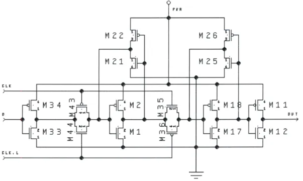
2.4.3 Registers
Once again simplicity and reliability were chosen over more complicated
circuitry, and a static "jam" register was chosen.
8No dynamic gates are used, so
charging is not an issue. This design also employs weak feedback inverters, which
reduces the load on the clock. A schematic of this register can be seen in Figure
2-5.
2.4.4 Multiplexor
The standard two-input multiplexor was designed using transmission gates. It can
be seen in Figure 2-4.
... .. ... ...
M0 U T
M I
-W5
MZ2
Figure
2-5:
Jam Register Schematic and Layout
CLK
LK. L
Ml1
DUT
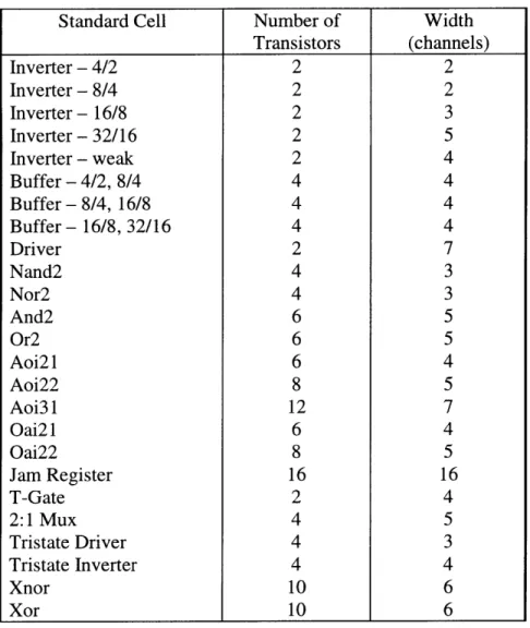
Table 2-1: Standard Cell List
Standard Cell
Number of
Width
Transistors
(channels)
Inverter
-
4/2
2
2
Inverter
-
8/4
2
2
Inverter
-
16/8
2
3
Inverter - 32/16
2
5
Inverter
-
weak
2
4
Buffer
- 4/2,
8/4
4
4
Buffer - 8/4, 16/8
4
4
Buffer - 16/8, 32/16
4
4
Driver
2
7
Nand2
4
3
Nor2
4
3
And2
6
5
Or2
6
5
Aoi21
6
4
Aoi22
8
5
Aoi31
12
7
Oai21
6
4
Oai22
8
5
Jam Register
16
16
T-Gate
2
4
2:1 Mux
4
5
Tristate Driver
4
3
Tristate Inverter
4
4
Xnor
10
6
Xor
10
6
Chapter 3
The Place and Route Tool
Once the standard cell library was in place, the next step was to create the
algorithm that would use these standard cells to create a design. This chapter focuses on
the Lisp program that was created by several people in order to perform this task. This
program, magic.scm, can be found in the appendix. An overview of the basic strategy
was presented in chapter 2, so one is not given here. The first section of this chapter
discusses the method adopted to solve this problem. Section two focuses on how this
algorithm performs placement. Section three then details how routing is done.
3.1 Program Methodology
The members of this group decided that the most natural way to think about the
various parts of this problem was as objects. Thus, the basic strategy employed is to
convert magic files into data objects, manipulate them to create a design, and then
convert this back into a Magic file. Finally, an attempt was made to make this tool
functional in any process, rather than just the particular one used by this project. As a
result, there is a section that assigns design rule parameters that are essential to this tool
to the corresponding values for a specific process. So if the designer changes processes,
they can simply change the value of these global variables, and the program will still
work optimally, without creating design errors.
The first section of magic.scm contains the object definitions, as well as
procedures to access these objects. One of the major objects is a magic-file. This object
consists of additional objects: layers, one of the possible paint layers in Magic, such as
poly; uses, or subcells; and labels, which are names used to label nodes in a circuit. Each
of these objects also has several procedures associated with it, such as instantiate-use,
which is used to add a subcell to the current layout. As the reader will see shortly, this
procedure is used in performing layout. Another object is a magic-box, which is a vector
consisting of coordinates for the four comers of a box. This object is used to specify
where to add paint to the layout, such as in wiring. Finally, there are two procedures,
read-magic-file and write-magic-file, which are used to convert between this data
representation of a layout and the Magic representation.
These are basically parsing
routines, which extract the desired information and format it appropriately.
3.2 Performing Placement
The next section of magic.scm deals with placement.
There are two main
procedures used to perform placement. The basic idea, as described previously, is to tile
together subcells. The approach taken here is to first create a horizontal row of cells,
which usually make up a single bit-slice. Then, these slices are tiled vertically, to create
the data path. This is done with two main procedures. First, instantiate-and-tile is used
to create a single bit, by specifying the horizontal direction. Then, one of two things is
done.
If the circuit being designed consists of identical bit-slices, then
instantiate-vertical-array can be used to create an array of the subcircuit just designed. If the bits are
different, then instantiate-and-tile can be used in the vertical direction.
Instantiate-and-tile-vertical-array was added after some use of this tool, in order to simplify the the task
of replicating a single subcircuit a large number of times.
Instantiate-and-tile takes in a number of arguments, including the direction in
which to tile. Most of the arguments are lists: uses-to-instantiate, or the subcells that the
designer wishes to tile together, in the order in which they will be tiled; instance-names,
or the names to be given to the particular instances of the uses you are tiling;
transform-generators, or transforms that you wish to apply to the instances you are tiling, such as
flipping them upsidedown or sideways; xoffsets and yoffsets, which are used to offset the
instances you are tiling in the x or y direction. The list of transforms is defined earlier in
this section of the code, and they are performed by transforming the coordinates of a use
appropriately. This algorithm then applies instantiate-use to each set of corresponding
entries of these lists. It also calculates the correct position at which to place the next
instance, by setting the variables xpos and ypos appropriately.
Instantiate-and-tile-vertical-array is very similar, except that it does some things to simplify the process of
creating an array. It takes in the name of the use you wish to instantiate and the number
of times you wish to instantiate it. It then creates the lists described above of the
appropriate length and calls instantiate-use on each set of the corresponding entries of
these lists. It does assume several things, such as the name for each instantiated use,
which is simply the name of the subcell with a number appended to it that corresponds to
the number of that particular instance in the array. By using these procedures, the user is
able to specify the exact placement of the subcells in their design.
3.3 Performing Wiring
The remainder of magic.scm deals with the task of connecting the placed uses
together. As described before, this tool divides the layout into vertical and horizontal
routing channels in order to perform the routing. There are two important routing tasks.
The first one is routing signals, or routing from one label to another. The second one is
routing power and ground via a large grid.
3.3.1 Routing Signals
Routing of signals is done via the procedure instantiate-wire. This procedure
takes as arguments the magic file being edited, the name of the use and the label in that
use from which the wire will start, the name of the use and the label in that use where the
wire will terminate, and a horizontal channel index. A label is a term Magic uses to give
a name to a rectangular area on a particular layer. They are used to indicate where the
"pins" for each cell are located. The procedure then routes a wire consisting of a metal3
horizontal wire in the specified channel, and metal2 vertical wires from the specified
labels to this horizontal wire, with contacts at the intersections of these wires. These
metal2 wires are painted in the vertical channel in which their labels occur.
As
mentioned previously, wires are created by making boxes and filling them in with the
appropriate metal.
Instantiate-wire performs the above task by calling several other procedures. It
uses instantiate-vertical-wire-segment to make the vertical wires. This procedure creates
a box that spans from the center of the specified starting horizontal channel to the center
of the specified ending horizontal channel in the specified vertical channel. This box is
centered in the vertical channel, and has a width equal to the minimum metal2 width.
This width is one of the previously mentioned global variables that is process-dependent.
The box is then filled with metal2. Next, instantiate-horizontal-wire-segment is used to
make the horizontal wire and the contacts. This routine is similar to
instantiate-vertical-wire, as it creates boxes and then fills them with the appropriate paint. The only
difference is that this box spans from the center of the starting vertical channel to the
center of the ending vertical channel, in the specified horizontal channel. Again, this box
is centered in the horizontal channel, and has a width equal to the minimum metal3
width. This procedure also uses instantiate-contact to place the contacts at the ends of
this wire. Instantiate-contact takes a layer, height, width, and vertical and horizontal
channel indexes as arguments. It then creates a box of the desired height and width
centered in the intersection of the specified channels and fills it with the specified layer.
There are several other wiring procedures that allow for more complicated wiring.
Instantiate-five-segment-wire is very similar to instantiate-wire, except it contains two
more jogs. In other words, the user specifies a starting horizontal channel, a vertical
channel, and then an ending horizontal channel. As before, the procedure routes from the
specified labels to this wire with vertical wires. It works very similar to the way
instantiate-wire does. This procedure can be used when the vertical channel that one of
the labels is in is already in use by another wire. Instantiate-single-layer-wire is another
wiring procedure, and it can be used to make a wire on a single layer. This works similar
to instantiate-wire, except it uses instantiate-specified-vertical-wire-segment
and
instantiate-specified-horizontal-wire-segment rather than instantiate-vertical-wire and
instantiate-horizontal-wire. This procedure is useful for routing between adjacent cells in
metall to save routing channels, where this is possible. There are two other procedures
instantiate-vertical-strap and instantiate-horizontal-strap that are very similar to one
another. They can be used to create a straight wire from one specified channel to the
next, in either the horizontal or vertical direction. These procedures create a
horizontal/vertical wire on the specified layer, in the specified horizontal/vertical channel,
and runs it from the left edge of the specified starting vertical/horizontal channel to the
right edge of the specified ending vertical/horizontal channel. This is useful for doing
things like tying a node to ground or VDD. These procedures enhance the basic
instantiate-wire command by allowing the designer to route several different types of
wires.
3.3.2 Routing Power and Ground
Power and ground are distributed across the chip by a grid whose properties are
set by the designer. As explained in section 2, all standard cells include metall power
and ground rails bordering the top and bottom, respectively. Thus, when cells are tiled
together horizontally and vertically, these create horizontal power and ground wires,
which are shared by adjacent rows. In order to handle large power requirements, rather
than butting each vertical row up against its neighbor, these can be spaced out. Then, the
space can be filled in with metall, effectively creating wider power and ground rails.
Since this program relies on the contacts within standard cells being on a grid in order to
perform signal wiring, all standard cells have to remain on grid. Thus, the width of the
horizontal rails must be increased in increments equal to the horizontal channel height.
In order to make power distribution even more efficient, the designer also has the ability
to add vertical metal2 wires to connect these horizontal power and ground rails. The
designer therefore has several options when routing power: they have the flexibility to
set the width of both the horizontal and vertical wires, as well as how frequently to place
the vertical connections. The final task that needs to be handled is the placement of
substrate contacts, which are placed in the center of the horizontal power and ground
rails, the minimum distance apart. Note that this happens to correspond to the vertical
grid spacing.
The task of routing power and ground is performed by the function
instantiate-power-grid. This procedure performs the three functions described above: it creates the
horizontal rails of the desired width, it places substrate contacts, and it routes the vertical
interconnections of the desired width and spacing. In order to do this,
instantiate-power-grid takes in three arguments: horizontal-channel-span is used to specify the width of the
horizontal wires, vertical-rail-spacing is used to specify the frequency of vertical rails,
and vertical-rail-width is used to specify the width of the vertical rails. The procedure
can be divided into three main parts according to the task that each part performs.
The first part of this procedure creates the horizontal rails. This is done with the
named-let instantiate-horizontal-rails. This routine walks down the specified layout from
top to bottom, painting horizontal metal 1 wires at the appropriate places. This is done by
calculating the topmost channel of the design, and then moving down the appropriate
number of channels in between wires, depending on the desired horizontal-channel-span.
In order to do the painting, it calls the previously mentioned procedure
instantiate-horizontal-strap. The starting and ending vertical channels are the leftmost and rightmost
channels of the design, which are also calculated by instantiate-power-grid.
The second part of this procedure is interleaved with the painting of these vertical
wires, and that is the placing of contacts. There are actually two types of contacts that
need to be placed, the substrate contacts and the metal2 contacts that will connect the
horizontal and vertical power wires together. These contacts are placed on a particular
horizontal channel after it has been painted. This is done with the named-let
instantiate-substrate-contacts. This section of the code walks across the particular horizontal wire in
minimum contact spacing increments, determines which type of contact to paint at each
location, and paints that contact. The determination of contact type is based on the
vertical-channel-spacing argument, which tells the program where vertical wires will be
going and thus where metal2 contacts need to be placed. The actual painting of the
contacts is done with the append-box routine, which creates a box at the specified
location and fills it with paint from the specified layer.
The final part of this routine is the painting of the vertical wires where
specified by the designer. These are painted by the named-let instantiate-vertical-rails.
This code once again walks across the entire layout horizontally. Only this time it paints
pairs of adjacent vertical metal2 wires, one from the topmost power rail to the
bottommost power rail and one from the topmost ground rail to the bottommost ground
rail, with each pair of wires spaced apart by the specified vertical-rail-spacing. The
painting of the vertical wires is done with instantiate-vertical-strap. The leftmost and
rightmost vertical rails are created separately, by another let function called
instantiate-vertical-boundary. This procedure walks down the entire design and paints two pairs of
metal2 wires at each standard cell row location. It uses instantiate-vertical-strap to add
wires from the current set of horizontal power and ground rails to the power and ground
rails just below, on both sides of the design. This in effect creates vertical wires that run
the length of the design and are connected to every horizontal power or ground rail. It is
in this way that the power grid is created on a given layout.
Chapter 4
Data Path Elements
After developing the standard cell library and place-and-route tool, the next step
was to use these to construct the components necessary for data path design. The idea
was to create a set of data path elements that would be used in the processor, as well as
future data path designs. These included elements such as a 32-bit adder and a 32-bit
register. Rather than describe each of these blocks, this chapter will instead focus on the
design and construction of one such component, the 32-bit adder. It is hoped that this
will give the reader a better understanding of how this tool is used to construct circuits.
The first section will describe the types of adder designs investigated for this project, and
explain the design of the adder circuit that was finally chosen. Section two will then
explain how the new tool was used to construct this adder out of standard cells. Section
three concludes the chapter by commenting on other blocks that were constructed in a
similar fashion.
4.1 32-Bit Adder Design
Addition is the basis for many processing operations. As a result, an adder is an
important part of a data path cell library. A wide variety of implementations exist, and
the choice as to which one to use depends on speed and density requirements. A variety
of adders were designed and simulated for this project, and in the end a binary look-ahead
carry adder was chosen.
4.1.1 Binary Full Adder
The familiar equations for a binary adder, where A and B are the summands, Cin
is the carry input, S is the sum output, and Cot is the carry output are:
S
=
A
B
@Cin
Cout
=
AB
+ Cin(B+A)
These can be factored into the alternative form:
S
=
P
Cin
Cout
=
G
+PCin
where
G
=
AB
generate signal
P
=
A
B
propagate signal
4.1.2 Ripple-Carry Adder
The simplest 32-bit adder design consists of 32 full adders chained together. The
above full adder equations can be implemented with the following gates:
F - A c
While small and simple, this adder is slow, due to the long carry chain. However, it does
provide a base on which to compare the speed of more complicated adders.
4.1.3 Carry-Skip Adder
The worst-case delay for a ripple-carry adder occurs when a carry is generated in
the lowest order bit and must propagate through the entire adder. One way to improve
this delay is to "skip" the carry over a block of full adders if the propagate signals for
each bit in the block are high.
9This design consists of a ripple-carry adder divided into
blocks, where a special circuit associated with each block quickly detects if all the bits to
be added are different (Pi
=
1 for all bits). In this case, the carry entering into the block
may directly bypass it and be transmitted into the next block. It is also worth noting that
if Ai=Bi for some i in the block (Pi
=
0), no block is skipped, but a carry is generated in
that block. Thus, the carries are propagated in parallel, and the total time of computation
is bound by the time of carry propagation in the largest block.
The carry-skip block is actually just the AND of every Pi in a given block. Since
the fan-in of this AND gate equals the number of bits in a block, optimal block sizes are 3
or 4 bits. Additional improvement can be achieved by adding additional layers of skip.
These layers would then skip multiple blocks, and they are conveniently identical in
construction to lower skip levels. An optimal scheme consisting of two levels of skips
was determined and tested.
It was found that the speed of this adder was limited
4.1.4 Manchester Adder
Another method commonly used to improve the speed of addition is a Manchester
carry chain.
'
1The objective behind this design is to propagate the carry as fast as
possible, by using Pi and Ci to either propagate or generate a carry for each bit. One way
to do this is with a multiplexor in the following configuration:
-?II
Figure 4-2: Manchester Carry Adder Schematic
However, such circuits rapidly slow down as bits are chained together, due to the
resulting chain of transmission gates. So once again, the adder is divided into blocks and
separated with restoring inverters. With the gates used for this project, the optimal block
size was found to be 3. A further improvement can also be gained by applying the skip
idea from before. Once again, blocks of bits can be skipped if all of the bits in a block
are propagating a carry. The skip circuitry chosen for this design was a "conflict-free"
circuit, which improves the speed by using a 3-input multiplexer that prevents conflicts at
the wired OR node in the adder. This can be seen in Figure 4-3. The control signals T1,
-Pi -Ti
Figure 4-3: Conflict-Free Manchester Carry Skip Circuitry
This idea of skipping bits can also be applied to the resulting blocks.
A 32-bit
manchester adder with carry skip as described was constructed, and it turned out to be
quite fast. This design consists of ten 3-bit manchester-skip blocks in series, with a full
adder tacked onto the front and rear of this array. Then, block-skip circuitry is added on
top of this, as can be seen in Figure 4-4. Once again, the rate-determining element turned
out to be the skip circuitry, which became slow for large fan-in or significant loads.
Thus, the buffering inverters must be kept small.
Figure 4-4: 32-Bit Manchester Carry-Skip Adder Schematic
4.1.5 Binary Lookahead Carry Adder
The idea behind this adder is to improve the linear growth of carry delay with the
size of the input for an n-bit adder by calculating the carries for each stage in parallel.
The carry for the ith stage, Ci, may be expressed as
Ci = Gi + PiCi-I
Expanding this yields
Ci
=Gi + PIG,
1+ PiP,-G,-2+ ... + P...P
1C
0The size and fan-in of the gates needed to implement this carry-lookahead scheme
becomes quite large as the number of bits increases. One alternative to this method is to
compute the carries in a binary fashion." Define a new operator # such that :
(g
1,p
1) # (g2
,
2) = (g
1+ 91gl, P1P2).
It can be seen that the carry signals can be determined
by G,, where
(Gi,P,)
=
(gl,p
1)
if i=1
(g,p,) ... # ... (G,,Pi.)
if 2 <i < n
(g,, p,) # (g,- ,P,-1) ... # ... (gi,pi)
In other words, by combining the p,'s and g,'s from two input bits, or the results
from two previous combinations of such signals, the carry bits are constructed in a binary
PG
BLOCK
G
32
P
32
CARRY
EVALUATION
BLOCK
C
32
SUM
BLOCK
Figure
4-5:
Binary Look-Ahead Carry Adder Block Diagram
The generate/propagate block simply consists of the logic required to compute P
and G and can be seen in Figure 4-6. The sum block consists of an array of XNOR's.
The carry block consists of the logic required to implement the # function. In order to
improve speed and reduce the number of gates, we can complement alternating # blocks.
These blocks can be seen in Figure 4-7, as BA and BB.
Figure 4-6: GP Block Schematic
Figure 4-7: BA and BB Block Schematics
The carry evaluation block then looks like Figure 4-8 for a four-bit adder. This
pattern is then iterated to create the carry block for an adder of the desired size. Since
two bits are combined at each stage, a binary tree is formed, and thus the speed of this
adder is proportional to log
2(n). Another nice feature of this adder is that it is very
wiring. Such an adder was designed and built, and it was the fastest of the previously
mentioned adders.
One of the limiting factors of such an n-bit adder is that the most significant '#'
operator in each of the j columns of the carry evaluation block must drive 2
"#"
blocks in
the next stage. As n gets large, this can be a considerable load, as j=log
2(n). Thus,
buffering of such signals becomes very important. One approach to this problem is to run
these outputs directly to the most-significant "#" block in the next stage, while
simultaneously buffering them to the remaining "#" blocks. This will maximize the
speed at which these outputs reach the most significant block, which turns out to be the
critical path. In the design used for this project, various sizes of inverters were used to
perform this buffering. In the second to last stage, for example, a buffer consisted of a
16/8 inverter followed by a 32/16 inverter. A schematic for the 32-bit BLCA Adder can
be seen in Figure 4-9.
P30 UT P34 C34 l 93 >3PUA P POUT P UT C3OUT PH P P c " c cUT ..- C 0 0 T P PU-0P30UT BA c CO -CD C
Figure 4-9: 32-Bit BLCA Adder Schematic
4.1.6 Final Results
Table 4-1: 32-Bit Adder Results
32-Bit Adder Style
Computation Time (ns)
Ripple-Carry Adder
8.5
Carry-Skip
3.5
Manchester Carry Chain
6
Manchester Carry Chain with skip
2.7
Binary Carry-Lookahead
2.1
These results are from a schematic-capture program, which was then used to generate
Spice files. This program does not take all capacitances into account. Each circuit was
tested in the bottom left process corner, with a Vdd of 3V and a temperature of 125 C.
4.2 Layout of the 32-Bit Adder
The organization of the adder in layout corresponds very closely to the schematic.
The generate/propagate logic lines the far left, the array of XNOR's is on the far right,
and the columns of the carry block are in the middle. One convenient feature of this
adder is that the carry buffers fit nicely under the subsequent columns of the carry block,
as can be seen in the Figure 4-10.
All of the necessary leaf cells already existed in the standard cell library, so the
only thing that needed to be done was to place and route them. The 32-bit adder contains
large amounts of redundancy, so it was constructed in such a way as to maximize the
power of the place-and-route tool. First, the GP, BA, and BB blocks were constructed.
One feature worth pointing out is the overlap of the two cells that make up BA, which is
a nice feature supported by the place-and-route algorithm. Then, the carry block for a
two-bit adder was constructed out of these pieces and connected to two GP blocks. As
can be seen from the schematics, the carry block for a four-bit adder is simply a pair of
two-bit adders, with an additional column of BA's on the top two bits. Moreover, an
eight-bit adder consists of a pair of four-bit adders, with an additional column of BB's on
the top four bits, and so on. This is the method that was used to construct the GP and
carry block sections of the 32-bit adder. One detail that must be attended to is the
polarity of the inputs to the BA and BB blocks. If there are ever two consecutive BA or
BB blocks, then the outputs of the first one must be inverted before they are input into the
second one. These inverters were put wherever there was space, which was usually
underneath the carry buffers. Finally, an array of 31 XNOR's and an inverter were
appended to the right of the carry block, in order to generate the SUM and C31 outputs
(only 31 XNOR's are required because SO is just PO when there is no Cin).
4.3 Additional Blocks
The other necessary blocks were constructed in a similar manner. However, the
adder was the one block that involved significant research in the area of circuit design.
Unlike the adder, the other blocks were based on the schematics for a
previously-designed processor. The only major difference between these is transistor sizes, due to
the switch from custom hand layout to standard cells.
IIWO x -1 • .. ... 'M V!, RA I lxx ,V4%
Figure 4-10: 32-Bit BLCA Adder Layout
8~~ thiM MD tdWrd~
am_ a
i. a
M -:i d