Bias Temperature Instability (BTI) in GaN MOSFETs
by
Alex Guo
B. S. in Electrical Engineering and Computer Sciences,
University of California, Berkeley, 2010
S.M. in Electrical Engineering and Computer Science,
Massachusetts Institute of Technology, 2012
Submitted to the Department of Electrical Engineering and Computer Science
in partial fulfillment of the requirements for the degree of
Doctor of Philosophy in Electrical Engineering
at the
Massachusetts Institute of Technology
September 2016
0 2016 Massachusetts Institute of Technology
All rights reserved
MASSACHUSETTS INSTITUTE OF TECHNOLOGY
SEP 28 2016
LIBRARIES
ARCHI
Signature redacted
Signature of Author
...
Department of Electrical Engineering and Computer Science
Aug 12, 2016
C ertified by
...
Signature redacted
Jesu's A. del Alamo
Professor of Electrical Engineering
Thesis Supervisor
A ccepted by ...
Signature redacted
/
,&i A. Kolodziej ski
Bias Temperature Instability (BTI) in GaN MOSFETs
By Alex Guo
Submitted to the Department of Electrical Engineering and Computer Science On August 12, 2016 in partial fulfillment of the requirements for the degree of
Doctor of Philosophy in Electrical Engineering
Abstract:
GaN is a promising alternative to Si for transistors for power electronics. For high-voltage applications, the GaN high electron mobility transistor with insulated gate (MIS-HEMT) is an attractive transistor structure because of its high breakdown voltage combined with low gate leakage current. Impressive device performance has recently been reported. However, before
GaN MIS-HEMTs cab be deployed in the field, reliability and stability issues need to be solved.
In particular, the threshold voltage (VT) instability under high voltage and temperature stress, sometimes referred to as bias-temperature instability (BTI), is a serious concern. The physical mechanisms responsible for BTI in GaN MIS-HEMT are not well understood. This is mainly because of the complex gate stack with multiple layers and interfaces, which presents many trapping sites with complex dynamics. In this work, a simpler GaN MOSFET structure is used to isolate the role of the gate oxide and the oxide/GaN interface in BTL.
Using a carefully designed benign characterization approach, we have studied in detail the response to positive and negative gate bias stress of GaN MOSFETs with various gate dielectrics. This has allowed us to postulate relevant physical mechanisms. For positive gate stress (PBTI), positive VT shifts are caused by a combination of electron trapping in pre-existing oxide traps and trap generation either at the oxide/GaN interface (SiO2/GaN) or in the oxide close to the
interface (A1203/GaN). For negative gate stress (NBTI), three degradation mechanisms are proposed. In low-stress regime, recoverable electron detrapping from pre-existing oxide traps takes place resulting a temporary negative VT shift. In mid-stress regime, a transient positive Vr
shift is probably caused by electron trapping in the GaN channel under the edges of the gate. In high-stress regime, there is a permanent negative VT shift, which is consistent with interface state generation. In addition, we have confirmed that for benign positive and negative gate bias stress, there is a unified reversible mechanism that accounts for the device dynamics and that is electron trapping/detrapping in pre-existing oxide traps. This work provides fundamental understanding
to elucidate the reliability and instability of high-voltage GaN MIS-HEMTs.
Thesis supervisor: Jesus A. del Alamo
Acknowledgments
This thesis would not have been possible without the guidance and support from many people around me. First, I would like to express my sincere gratitude to the most wonderful research advisor, Prof. Jesus del Alamo. I still cannot believe how lucky I am to be one of his students. For the past six years, Prof. del Alamo has continuously encouraged me, supported me, and guided me through many research obstacles. I have benefitted tremendously from his teaching in and out of the classroom. His attention to detail and passion for advising are essential elements that made this work possible. I also would like to thank my thesis readers, Prof. Dimitri Antoniadis and Prof. Tomas Palacios. Their valuable feedback and insights helped me greatly in completing this thesis. I would like to thank our industrial sponsor, who provided test chips for this work. I have also benefited tremendously from our collaborations throughout the course of this study.
The MIT Microsystems Technology Laboratories is my research family, and I would like to thank those who have helped me along the way. My current research group members: Alon, Xiaowei, Shireen, Yufei, Xin, Wenjie, and Elizabeth. Group alumni: Jungwoo, Jorg, Ling, Luke, Donghyun and Jiangqiang. MTL administration staff: Debb, Valerie, Mara, and Sherene. MTL staff members: Bill, Bob, Dave, Dennis, Donal, Eric, Kurt, Mark, Mike, Pat, Paudely, Paul M., Paul T., Scott, and Vicky. I would like to thank them for their friendship and support throughout my time at MTL.
At MIT, I have been very lucky to meet a group of wonderful friends. They have been there for me during good times and bad, helped me overcome personal difficulties, and more importantly, made me a better version of myself. Today, I cannot imagine my life without their friendship. I want to give special thanks to the following individuals: Wardah, Richard, Robert, Mikhail, Bomy, Ina, Nina, Eva, Julie, Caleb, Kendall, Dan, Sven, Connie, Lulu, Jouha, Laura, Gregorio, Fabio, and Rohit. Thank you all for making my life at MIT such an enjoyable one!
Finally, I would like to thank my longtime friends, Renata, Liana, and Helen for their love and support. Last but not least, I am thankful for my family back in China. My grandparents who raised me, my parents, sister, brother-in-law, and my little nephew, thank you for being an important part of my life. I love you all.
This work was sponsored by the MIT!MTL GaN Energy Initiative and the United States National Defense Science and Engineering Graduate Fellowhip (NDSEG)
Contents
Chapter 1. Introduction...
19
1.1. Motivation of Reliability Study of GaN MIS-HEMT ... 19
1.1.1. Overview of GaN MIS-HEMT technology ... 19
1.1.2. Reliability challenges of GaN MIS-HEMTs... 20
1.2. Bias Temperature Instability (BTI) in GaN MIS-HEMTs ... 22
1.2.1. BTI in Si, SiC and other III-V systems... 22
1.2.2. Current understanding of BTI in GaN MIS-HEMTs ... 25
1.2.3. Advantage of GaN MOSFET structure... 26
1.3. Thesis Goal and Organization ... 27
Chapter 2. Experim ental ...
29
2 .1. Introd uction ... 29
2.2. Device Structure and Figures of Merit ... 29
2.3. Experimental Setup ... 31
2.4. Experimental Design ... 32
2.4.1. The need for a benign BTI characterization scheme ... 32
2.4.2. FOM extraction, device detrapping, and initialization ... 34
2.4.2. Standard experiment flow... 36
2.4.2. Experiment flow variations... 38
2.5. Chapter Summary... 40
3. 1. Introduction ... 43
3.2. Experimental Results of SiO 2 Devices ... 45
3.2.1. Effect of positive gate bias stress at room temperature ... 45
3.2.2. Im pact of stress tem perature ... 48
3.2.3. SiO2 devices summ ary ... 51
3.3. Experimental Results of Si0 2/Al203 vs. SiO2 Devices
...
513.4. Discussion ... 55
3.4.1. M echanisms responsibility for VT shift under PBTI ... 55
3.4.2. M odel...59
3.5. Chapter Sum m ary... 62
Chapter 4. Negative-Bias Temperature Instability (NBTI)...63
4. 1. Introduction ... 63
4.2. Overview : A Three-Regim e Behavior ... 65
4.3. Experim ental Results and Discussion of SiO2/Al2O 3 Devices ... 66
4.3.1. Regim e 1 (low-stress) ... 66
4.3.2. Regim e 2 (mid-stress)... 69
4.3.3. Regim e 3 (high-stress)... 75
4.4. SiO2 vs. SiO2/Al2O3 Devices... 78
4.4.1. Effect of Negative Bias Stress at Room Temperature ... 79
4.4.2. Im pact of Stress Temperature ... 82
4.5. Chapter Sum m ary... 85
Chapter
5.
PBTI-NBTI Continuum in SiO
2/A1
2O
3MOSFETs...87
5. 1. Introduction ... 87
5.2. Experimental Results... 89
5.2.1. Benign gate bias stress at room temperature (RT)... 89
5.2.2. Impact of tem perature... 91
5.3. Discussion ... 95
5.4. Chapter Summary... 100
Chapter 6. Conclusion...101
6.1. Thesis Summary and Key Contributions... 101
6.2. Suggestions for Future Research... 104
List of Figures
Figure 1-1. Cross section of a typical AlGaN/GaN MIS-HEMT structure (not to scale). ... 22
Figure 1-2. Two types of model: defects are located (a) at the Si02 /HfO2 interface [38] or (b) in the bulk of high-k film [41]. ... 24
Figure 1-3. (a) Overview of potential defect centers in the oxide/barrier gate-stack of a GaN MIS-HEMT device. (b) Bias effect on defect energy position of bulk oxide defects as a function of the depth x [18] ... 26
Figure 1-4. GaN MOSFET structure used in this thesis. ... 27
Figure 2-1. Cross section of GaN MOSFET used in this work. ... 30
Figure 2-2. Schematic diagram of experimental setup. ... 31
Figure 2-3. (Symbols) Comparison of VT shifts during NBTI stress for fast (tdeiay = 100ps) and slow (tdieiay = Is) sensing at stress voltages of -1.5V and -2.5 V. The (lines) values n are determined by a fit to a power law AVT t" [56]... 33
Figure 2-4. Minimal AVT and AS after 50 continuous short ID-VGS Sweeps... 34
Figure 2-5. Room temperature subthreshold characteristics in the linear regime (VDs = 0.1 V) before stress, after stress, after thermal detrapping (TD), and after 4 months of storage... 35
Figure 2-7. Stress and recovery sequence and device FOM extraction during ramps. (a) Continuous ID-VGS sweeps for FOM extraction during recovery. (b) During recovery, the gate and drain voltage are forced to be 0 V. ID-VGS sweeps are periodically measured during recovery. ... 37
Figure 3-1. Subthreshold and transconductance characteristics of (a) SiO2 and (b) SiO2/A1203
GaN MOSFETs in the linear regime (VDS = 0.1 V) at different temperatures. ... 44
Figure 3-2. Stress time evolution of AVT and AS for Si02 GaN MOSFETs stressed at three
different voltages at room temperature. Data points are taken 1 see after the stress. The last set
of points (open symbols) are AVT and AS after thermal detrapping following a stress experiment
w ith tstress = 10,000 S... 45
Figure 3-3. Stress time evolution of AVT and AS for Si02 GaN MOSFETs stressed at three
different voltages at room temperature. The first data point in the sequence is taken 1 sec after
the stress is halted. The last set of points (open symbols) are AVr and AS after thermal
detrapping following a stress experiment with tstress = 10,000 s. ... 46 Figure 3-4. Room temperature subthreshold and transconductance characteristics before and after VGS,stress = 15 V stress followed by thermal detrapping (TD) of SiO2 GaN MOSFETs in the
linear regim e (V DS = 0.1 V ). ... 46
Figure 3-5. Stress time evolution of IG for Si02 GaN MOSFETs stressed at three different
voltages at room tem perature... 47
Figure 3-6. Stress time evolution of Agm,max/gm,maxo for SiC2 GaN MOSFETs stressed at three
different voltages at room temperature. Data points are taken -1 see after the stress is paused.
The last set of points (open symbols) are Agmmax/gm,maxo after thermal detrapping following a
tstress = 10,000 s stress experim ent... 48
Figure 3-7. Stress time evolution of AVr and AS for Si02 GaN MOSFETs at different T.
VGS,stress = 10 V. Data points are taken 1 sec after the stress. The last set of points (open symbols) are AVT and AS after a thermal detrapping step that follows stress experiments with
Figure 3-8. Stress time evolution of AVT and AS for SiO2 GaN MOSFETs at different T.
VGSstress = 15 V. Data points are taken 1 sec after the stress. The last set of points (open symbols) are AVT and AS after a thermal detrapping step that follows stress experiments with
tstress = 10 ,000 S... 50
Figure 3-9. Recovery of AVT and AS after a 10,000 sec stress at VGSstress = 10 and 15 V for SiO2 GaN MOSFETs at 40'C, RT and 75'C. The last set of points (open symbols) is AVT and AS
after subsequent therm al detrapping step... 50
Figure 3-10. Stress time evolution of AVr for SiO2 vs SiO2/A1203 GaN MOSFETs at different T.
VGS,stress = 15 V. Data points are taken 1 sec after the stress. The last set of points (open symbols) are AVT after a thermal detrapping step that follows stress experiments with tstress = 10 ,000 s... 52
Figure 3-11. Stress time evolution of AS, for Si02 vs. SiO2/A1203 GaN MOSFETs stressed at
three different voltages at room temperature. Data points are taken 1 sec after the stress. The last set of points (open symbols) are AS after thermal detrapping following a stress experiment w ith tstress = 10,000 S... 53 Figure 3-12. Stress time evolution of Agm,max/gmmaxo for SiO2 vs. SiO2/A1203 GaN MOSFETs
stressed at three different voltages at room temperature. Data points are taken -1 sec after the
stress is stopped. The last set of points (open symbols) are Agm,max/gm,maxo after thermal
detrapping following a tstress = 10,000 s stress experiment. ... 53
Figure 3-13. Values of AVT after stress and final AVT after thermal detrapping vs. stress time for SiO2 vs. SiO2/A1203 GaN MOSFETs stressed at VGS,stress = 15 V at room temperature. ... 55
Figure 3-14. Final values of (a) AVT and (b) AS after thermal detrapping vs. stress time for SiO2
vs. SiO2/A1203 GaN MOSFETs stressed at three different voltage at room temperature. ... 56
Figure 3-15. Evolution of final values of AVr vs. AS for SiO2 transistors after VGS,stress = 15 V at
different temperatures. All measurements were taken at room temperature after a thermal
Figure 3-16. Evolution of Agni,max/gni,maxo vs. AVT for SiO2 and SiO2/A1203 transistors during
stress experiments of various durations at room temperature. The open symbols correspond to measurements after a thermal detrapping step following stress experiments with tstress = 10,000 S. ... 5 8
Figure 3-17. Model vs. experiments of AVTOx evolution with stress time, for VGS,stress = 5 V, 10 V , and 15 V, at different tem perature. ... 61 Figure 4-1. AVT and AS as a function of stress time for VGS,stress = -10 V at 175'C. AVr and AS
taken 1 s after stress removal using short ID-VGS sweeps. The open symbols at the end indicate
final AVT and AS after a benign thermal detrapping (TD) step. ... 66
Figure 4-2. AVT and AS as a function of stress time (extracted 1 s after removal of stress) and
during subsequent recovery, for VGS,stress = -1, -3 and -5 V at RT. Open symbols at the end of
recovery represent AVr and AS after thermal detrapping (TD)... 67
Figure 4-3. ID-VGS and CG-VG characteristics of a device before stress, after stress and after thermal detrapping (TD), for VGS,stress = -I V, tstress = 10,000 s at RT. ... 68 Figure 4-4. Stress time evolution of IAVrI for VGS,stress = -1 to -2 V, at -40'C, -100C and RT.... 69
Figure 4-5. AVT and AS as a function of stress time (extracted 1 s after removal of stress) and
recovery time, for VGS,stress = -5 V at -450C, RT and 1250C. Recovery is traced after 10,000 s
stress using short ID-VGS sweeps... 70
Figure 4-6. Correlation of AVT and AS during stress and recovery for VGSstress = -5 V at 1250C. AV T and AS are linearly correlated ... 71
Figure 4-7. Stress time evolution of AVT, AS and Agm,max for (a) VGS,stress = -10, -15 and -20 V at RT, and (b) VGS,stress = -10 V at RT, 75'C, 1000C, 125'C... 72
Figure 4-8. CGSD -VG characteristics before and after VGS,stress = -20 V at RT for 1,000 s and after subsequent thermal detrapping. The body is floating... 73
Figure 4-9. (a) Zener trapping mechanism as suggested in [69]. Electrons tunnel from the valence band into defect states (ET) under high vertical electric field in the GaN channel caused
by high reverse bias stress. (b) Electrons are trapped in the GaN channel under the source and
drain edges of the gate. (c) High electron trapping lifts up the energy bands at the surface of the GaN channel shifting the threshold voltage positive under the edges of the gate and effectively increasing the local hole concentration. After stress removal, electron detrapping takes place through therm al processes...74
Figure 4-10. AVT, AS and Agm,max (a) immediately after stress at RT for VGS,stress = -10, -30, -50
and -70 V, and (b) after thermal detrapping performed along the same experiment... 76
Figure 4-11. AVT, AS and Agm,max after thermal detrapping at different times in stress experiments. VGSstress = -70 V and T = -45 C, RT and 1250C. ... 76 Figure 4-12. Correlation of (a) permanent AVT and permanent AS and (b) permanent Agm,max
and permanent AS for VGS,stress = -50 and -70 V at different T... 77
Figure 4-13. ID-VGs and C-V characteristics of a device before stress, after stress and after
thermal detrapping (TD), for VGS,stress = -70 V for tstress = 500 s at 125'C... 77
Figure 4-14. AVT and AS as a function of stress time for VGS,stress = -20 V at RT. The open
symbols at the end indicate final AVT and AS after a benign thermal detrapping (TD) step. ... 80
Figure 4-15. AVT and AS are linearly correlated during stress and recovery for VGS,stress = -20 V
at R T ... 80
Figure 4-16. AVT and AS as a function of stress time for VGS,stress = -10 V, -20 V and -30 V at RT. The open symbols at the end indicate final AVT and AS after a thermal detrapping (TD) step ... 8 1
Figure 4-17. Correlation of AVT and AS in Si02 devices during stress and recovery for VGS,stress
= -10 V, -20 V and -30 V at RT. AVT and AS are linearly correlated. ... 81
Figure 4-18. AVT and AS as a function of stress time for VGS,stress = -10 V at 125'C. The open symbols at the end indicate final AVT and AS after thermal detrapping... 82
Figure 4-19. Correlation of AVT and AS during stress and recovery for VGS,stress = -10 V at 125'C. For the SiO2/A1203 MOSFET, AVT and AS are linearly correlated. For the SiO2
MOSFET, AVT and AS seem to be reversely correlated... 83
Figure 4-20. AVr and AS as a function of stress time for VGSstress = -7.5 V at 125'C, -10 V at
125'C and -10 V at 175'C. The open symbols at the end indicate final AVT and AS after thermal detrapping . ... 84 Figure 4-21. Correlation of permanent AT and AS during stress and recovery for all experiments
reported in this w ork... 84
Figure 5-1. Stress time evolution of AVr, AS and Agm,max for VGS,stress from -5 V to 5 V at RT.
The last set of points (open symbols) are AVT and Agm,max after thermal detrapping. ... 90
Figure 5-2. AVT and Agm,max well correlated throughout stress and recovery, indicating similar m echanism . ... 9 1
Figure 5-3. Time evolution of AVT during stress and recovery at different T, for VGS,stress = 2 V and -2 V. The last set of points (open symbols) are AVT and Agm,max after thermal detrapping. 92
Figure 5-4. Time evolution of AVT during stress and recovery at different T, for VGS,stress = 2 V and -2 V. For PBTI stress, the first data points are removed to omit the effect of the fast mechanism. For PBTI and NBTI recovery, data are normalized to the first data points to show T
dependence... 93
Figure 5-5. Arrhenius plot of AVT change rate for PBTI/NBTI stress and recovery. RvT represents AVT change rate on log scale... 94
Figure 5-6. Energy band diagram of GaN MOSFETs under PBTI/NBTI stress and recovery... 95
Figure 5-7. Model vs. experimental data of AVT evolution with stress time at RT, for (a) VGS,stress from 1 V to 5 V, and (b) VGS,stress from -1 V to -5 V. Symbols are the experimental data, and solid lines are the m odel fitting results. ... 97
Figure 5-8. Model vs. experimental data of AVT evolution with stress time and recovery time at
Chapter 1. Introduction
1.1. Motivation of Reliability Study of GaN MIS-HEMT
1.1.1. Overview of GaN MIS-HEMT technology
AlGaN/GaN high electron mobility transistors (HEMTs) are promising to replace
conventional silicon devices for high-voltage switching applications [1], [2]. This is because the
wide energy band gap of GaN (3.4 eV versus 1.14 eV for silicon) enables a very high breakdown
field (3.5 MV/cm), which makes GaN devices the superior choice for high voltage operation. In
addition, the spontaneous piezoelectric effect in the AlGaN/GaN heterostructure creates a
two-dimensional electron gas (2DEG) with a density above 1013 cm2, forming a highly conducting channel without the need of doping [2]. These device properties allow low ON-resistance
operation, which significantly reduces power loss and make AlGaN/GaN HEMTs attractive for
many power electronic applications [1][3]-[6].
On the other hand, the AlGaN/GaN HEMT structure has two main limitations. First, gate
leakage is a major problem. Because GaN HEMTs are normally-ON, they are subjected to large
negative bias in the OFF-state. As a result, gate leakage becomes important when measuring the
OFF-state power loss. This also results in a reduction of the breakdown voltage [7]. It is
AlGaN/GaN HEMTs demonstrated so far have normally-ON (depletion mode) characteristics
with a negative threshold voltage (VT). This is not ideal for power applications because it
increases power loss during switching and also requires an additional driving circuit to ensure a
fail-safe system [9], [10].
To mitigate these two drawbacks, the AlGaN/GaN HEMT with an inserted insulating
layer, i.e., metal-insulator-semiconductor high-electron-mobility-transistor (MIS-HEMT) was
introduced [11]. With the added insulator, GaN MIS-HEMTs can achieve much lower gate
leakage current and in turn enable higher breakdown voltage than GaN HEMTs with a Schottky
gate [12]. In addition, GaN MIS-HEMTs also allow for VT modification to achieve
enhancement-mode (E-mode) operation (VT > 0) [13]. The increased breakdown voltage and the
possibilities of enhancement-mode operation make GaN MIS-HEMTs extremely desirable for
power switching applications. Recently, many studies have demonstrated GaN MIS-HEMTs
with superior performance over GaN HEMTs, and some studies have shown enhancement-mode
operation using gate insulating layers such as SiC2, A1203, HfO2 and AlN [14]-[16].
The new promising features of GaN MIS-HEMTs have attracted growing interest in
technology commercialization. However, the insulating layer also adds complexity to the gate
stack and introduces unwanted device instabilities on top of those existing in GaN HEMTs. In
the next section, we will discuss these reliability issues in detail.
1.1.2. Reliability challenges of GaN MIS-HEMTs
Reliability issues surrounding GaN MIS-HEMTs can cause temporary or permanent
device degradation, and this is detrimental to circuit performance and device lifetime. For
example, GaN MIS-HEMTs are normally operated under high drain-gate bias voltage, which
cause current collapse and an increase in ON-resistance [13][17]. Trapping at the
dielectric/semiconductor interface can also cause threshold voltage (VT) shift under various
biasing conditions [18]. Time dependent dielectric breakdown (TDDB) is another failure mode
that is critical to gate stack reliability [19]. These instabilities and reliability issues significantly
limit the usability of GaN MIS-HEMTs especially for high voltage and high frequency
operations.
There have been extensive studies on the subject of AlGaN/GaN HEMT reliability, but
very limited work has focused on the reliability of GaN MIS-HEMTs, especially in relation to
the gate stack [20]. Trapping and degradation mechanisms in GaN MIS-HEMTs are complicated
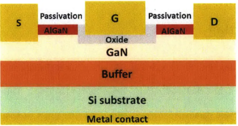
and not well understood. Figure 1-1 shows the cross section of a typical GaN MIS-HEMT
structure. The gate stack consists of the metal gate, the oxide layer, the GaN cap, the AlGaN
barrier and the GaN channel. As we can see from Figure 1-1, with the addition of an insulating
layer, the gate stack is quite complex with multiple interfaces. Studies on gate stack reliability of
GaN MIS-HEMTs have suggested multiple trapping sites in different layers and interfaces. For
example, Meneghini studied GaN MIS-HEMT with A1203/Si3N4 dielectrics (Si3N4 next to
AlGaN barrier layer) and found trapping behavior related to defects in the gate-drain region and
under the gate [211. Imada observed recoverable ON-resistance and threshold voltage shift under
positive gate stress of a recessed gate GaN MIS-HEMT with A1203 dielectric, which he
attributed to trapping at the. gate recess region [22]. Marcon focused on the time dependent
dielectric breakdown of GaN MIS-HEMTs with A1203/Si3N4 dielectrics (Si3N4 next to AlGaN
barrier layer), and proposed the mechanism of electron trapping below the gate [23].
Nevertheless, the physical origins of different trapping mechanisms are still unclear and needs to
S Passivation
G
PassivationD
Oxide
GaN cap
AIGaN
GaN
Buffer
Si substrate
Metal contact
Figure 1-1. Cross section of a typical AlGaN/GaN MIS-HEMT structure (not to scale).
In this thesis, we focus on the VT instability due to gate bias stress. This phenomenon is
often referred to as bias temperature instability (BTI) in standard CMOS technologies 1241. For GaN MIS-HEMTs, both depletion-mode (D-mode) and E-mode devices are subjected to gate bias stress during normal operating conditions. As such, VT shift under gate stress is a serious concern and needs to be studied carefully. In addition, it has been reported that BTI in GaN MIS-HEMTs is worse when compared to GaN HEMTs [251. Therefore, it is important to understand the contribution of the insulating layer and its interfaces to BTI of GaN MIS-HEMTs.
1.2. Bias Temperature Instability (BTI) in GaN MIS-HEMTs
1.2.1. BTI in Si, SiC and other III-V systems
BTI has been a critical reliability issue in MOSFETs made out of many material systems
such as Si, SiC and InGaAs. First observation of BTI for Si MOS transistors were made in 1966 1261. However, not until 2000's did BTI. particularly negative-bias temperature instability
(NBTI), become a serious concern. This happened because the introduction of nitrogen into the MOS fabrication process was found to enhance NBTI [27]-[29]. In advanced Si CMOS technology, NBTI has the greatest impact on p-FET devices due to the generation of positive
oxide charge and interface traps in MOS structures under negative gate bias, especially at
elevated temperature (1000 to 2500) [30], [31]. An increase in the absolute threshold voltage,
mobility degradation, drain current reduction and transconductance decrease are observed due to
NBTI [32]. One of the popular theoretical models for NBTI is the reaction-diffusion model (R-D
model) [27], [30], [33], [34]. In this model, the holes in the inversion layer interact with the Si-H
bonds at the oxide/Si interface. This interaction weakens the Si-H bonds and leads to
dissociation of H atoms with the corresponding generation of interface traps. In the diffusion
phase, hydrogen diffuses from the interface to the oxide. More recently, the R-D model has been
challenged by charge-trapping dominated theories such as the elastic hole trapping [35] and
switching oxide traps theory [36], where NBTI is explained by charge trapping and detrapping in
the oxide during the stress and recovery phases.
As CMOS technology continues to scale down, the use of high-k metal gate (HKMG)
becomes the key to extend Moore's law. Generally, a thin Si02 interface layer is needed
between the high-k dielectric and the channel to maintain high channel mobility [37]. High-k
dielectrics have created new challenges for the understanding of BTI, mainly due to pre-existing
traps in the oxide bulk [38]-[40]. Two separate models are proposed. for the possible location of
metal
Hft
S4 Si-fq
4
S
gate
gle
(a) (b)
Figure 1-2. Two types of model: defects are located (a) at the SiO2 /HfO2 interface [38] or (b) in the
bulk of high-k film [4
1].
To decide if the trapped charges are located in the bulk of the k film or at the high-k/interfacial layer, Young et al. performed hysteresis measurements on devices with different high-k thickness, and confirmed that trapping occurs mostly within the oxide bulk since less trapping in thinner high-k films is observed [42]. In a separate work, it has also been reported that under negative and positive gate bias, defects are charged and discharged through tunneling [43], suggesting that the responsible traps are very close to the device channel.
The methodologies and theoretical models developed for BTI in Si transistors constitute the foundation for reliability studies in newer material systems such as SiC and other 111-V compound based devices. For example, in SiC MOSFETs, it is observed that an alternating positive/negative gate stress with an electric field of I to 2 MV/cm across the oxide results in a repeatable VT shift/recovery [441. This is consistent with the BTI charge trapping theory for Si MOSFETs discussed earlier, and it is attributed to the large amount of near-interface oxide bulk traps tunneling in and out of the oxide. It is also reported that a decrease in the minority carrier
generation lifetime (partially recoverable) and increase in interface state density take place after
negative gate voltage stress in SiC MOS capacitors [45].
For other III-V devices such as InGaAs MOSFETs with high-k dielectric, it is found that
electron trapping at the pre-existing defects in the oxide contributes to a fast, recoverable
positive VT shift under positive gate stress [46]-[48]. In addition, stress-generated defects also
occur inside the oxide (A1203) in the near-interface region for InGaAs n-MOSFETs [47][48].
Studies on other high-mobility channel devices with high-k dielectrics also show similar charge
trapping phenomenon under positive gate stress [49]. In the meantime, a study on
ZrO2/A1203/InGaAs MOSFETs shows that a combination of trap-discharge and interface
degradation under NBTI caused a negative VT shift [50]. These BTI findings in SiC and InGaAs
transistors are largely consistent with those demonstrated in Si MOSFETs.
1.2.2. Current understanding of BTI in GaN MIS-HEMTs
Compared to other material systems, the understanding of BTI in GaN MIS-HEMTs is
very limited. There are a few studies that report VT shifts due to BTI in AlGaN/GaN
MIS-HEMTs [18], [51], [52]. In [18] and [51], authors use the concepts of CET maps to demonstrate
traps with a broad distribution of time constants, but the nature of the defect states is
inconclusive. It is suggested that the complex gate structure with multiple layers and interfaces
makes it challenging to isolate trapping effects from different layers and trapping sites. Figure
1-3 shows the complex nature of these trapping sites in the energy band diagram of a
MIS-HEMT structure. A few potential defect centers are suggested to contribute to VT drift: oxide
bulk defects, defects at the oxide/GaN interface and AlGaN barrier layer traps. A separate work
studied PBTI in GaN MIS-HEMTs [52]. Here, authors indicate that the oxide traps and the
MIS-HEMTs. However, the experimental data is limited to hysteresis analysis and the detailed
trapping process is unclear.
The complex nature of the gate stack makes it challenging to tackle the BTI problem in
GaN MIS-HEMTs. As such, the key to identify the physical origin of BTI in GaN MIS-HEMTs
is to isolate each trapping site and study their respective contributions to VT instability.
GaN
channel
'EF
GaN/AIGaN
barrier
(b)
metal
x+-S'02--
I
-thGaN
--
channel
GaN/AIGaN
barrier
Figure 1-3. (a) Overview of potential defect centers in the oxide/barrier gate-stack of a GaN MIS-HEMT device. (b) Bias effect on defect energy position of bulk oxide defects as a function of the depth x [181 .
0
1.2.3. Advantage of GaN MOSFET structure
What we have seen so far indicates that there are multiple trapping sites within the gate
stack that could contribute to BTI in GaN MIS-HEMTs, and traps in the oxide layer and at the
oxide/semiconductor interface are some of the key trapping mechanisms to investigate in order
to understand BTI in these devices. In this thesis, we use a simpler GaN MOSFET structure to
isolate the roles of oxide and the oxide/GaN interface to device instability in GaN MIS-HEMTs.
(a)
metal
S'0
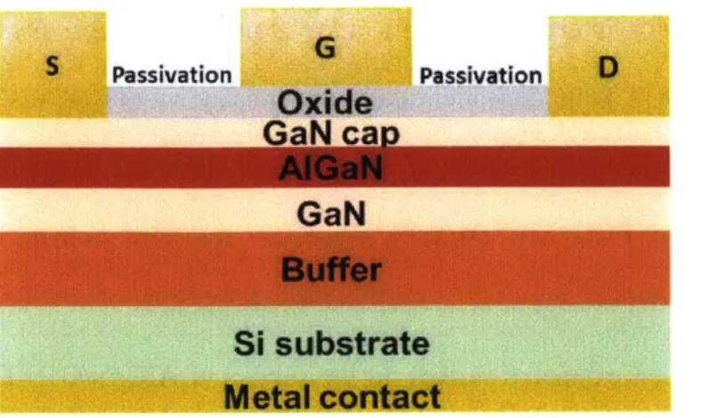
2Figure 1-4 shows the cross section of the GaN MOSFET studied in this work. In this
structure, the gate is recessed and the AIGaN barrier layer is etched away underneath the gate.
As a result, the GaN channel is located immediately below the gate oxide. The locations for
trapping are minimized and we can focus on the role of the oxide and the oxide/GaN interface.
This structure on its own is also a strong candidate for power electronic applications 1531, 154].
Passivation
G
Passivation D oxideGaN
Buffer
Si substrate
Metal contact
Figure 1-4. GaN MOSFET structure used in this thesis.
1.3. Thesis Goal and Organization
BTI is a major roadblock for technology commercialization of GaN MIS-HEMTs in
high-voltage power applications. This thesis takes a new approach to investigate BTI in GaN
MIS-HEMTs by focusing on the role of the oxide and the oxide/GaN interface using a simple
GaN MOSFET structure. The goal of this thesis is to provide a solid physical understanding that
can be used to mitigate BTI in GaN MOSFETs and MIS-HEMTs.
In chapter 2, we discuss the development of a benign characterization scheme that allows
the device figures of merit are described. Then, we present the details of the experimental setup
and the design process of our stress-recovery experiment flow.
Chapter 3-5 focus on experimental results and analysis of our BTI study. In chapter 3,
we present detailed experimental study of PBTI in GaN MOSFETs with SiO2 and SiO2/Al203
gate dielectrics. First, stress/recovery data of PBTI for various stress voltages and temperatures
in SiO2 MOSFETS are discussed. Next, we compare SiO2/A1203 MOSFETs against SiO2
MOSFETs and summarize their similarities and differences. We then perform a detailed analysis
of the experimental data and formulate hypothesis of the physical mechanisms behind PBTI.
In chapter 4, we study NBTI in GaN MOSFETs. An overview of a three-regime
behavior of NBTI in SiO2/A 2O3 MOSFETs is discussed first. Then, detailed experimental
studies of each of the three regimes in SiO2/A2O3 MOSFETs are presented. The hypotheses for
mechanisms behind the three regimes are discussed in detail. Next, we compare NBTI stress in
SiO2 versus SiO2/A1203 MOSFETs, and summarize our general findings.
Chapter 5 discusses a symmetrical continuum of PBTI and NBTI for low gate-bias stress
conditions. We show detailed measurement results of SiO2/A 2O3 MOSFETs for various low
gate stress voltage and temperature values and explain the physics behind the PBTI-NBTI
continuum.
Chapter 6 summarizes our key contributions to the understanding of BTI in GaN
MOSFETs. It also includes suggestions for future work to improve BTI and other device
Chapter 2. Experimental
2.1. Introduction
This chapter describes the experimental details of our BTI study on GaN MOSFETs. We
first developed a stress and characterization scheme for our test chips. This scheme allows us to
extract accurately device parameters before, during and after stress without affecting the device
figures of merit. This is important because device characterization itself could introduce
unwanted stress and shift device parameters.
This chapter is organized as follows. First, the GaN MOSFET structures used in this
work are presented. Next, we define the device's figures of merit that have been used to
characterize the effect of BTL. We then explain the details of a benign characterization scheme
we developed for this study. Following that, the standard experiment flow and measurement
variations for PBTI and NBTI are presented.
2.2. Device Structure and Figures of Merit
As stated in chapter 1, GaN MOSFETs constitute an excellent vehicle to study BTI in
GaN power FETs because it isolates the contributions of the gate oxide and the
are industrial prototype devices with a simple AlGaN/GaN recessed gate structures. The
cross-section of the device structure is shown in Figure 2- 1. The AlGaN barrier layer is removed from
the intrinsic gate region so that the gate oxide layer is in direct contact with the GaN channel.
The gate stack consists of either SiO2 or composite SiO2/A1203 dielectric (Al203 next to
semiconductor). The devices have channel width/length of 100 pm/I pm.
Passivation G Passivation D AIGaN AIGaN Oxide
GaN
Buffer
Si
substrate
Metal contactFigure 2-1. Cross section of GaN MOSFET used in this work.
In this work, we characterize the impact of gate bias stress at various temperatures on
device behavior through figures of merit defined in the linear operating region (at a drain-source
voltage (VDs) of 0.1 V). In particular, we focus our interest on the stability of three device
parameters: threshold voltage, VT, is defined at drain current ID = I p A/mm; subthreshold swing,
S, is defined at In = 0.1 p A/mm; and the maximum transconductance, grnrna, is defined as the maximum dID/dVGS obtained in an ID-VGs sweep. These three parameters are chosen to help us
understand how gate bias stress impacts charge control in the gate stack as well as channel
mobility so that the fundamental device degradation mechanisms as a result of BTI can be
For the most part, the devices under study have V1 around 0 V. However, throughout this
study, the fabrication process for our test chips has gone through various iterations. As a result,
there is batch to hatch variations of VT, S, and gihx. In virgin devices, V1 ranges trom -1 to 2
V, S from 100 to 250 mV/dec, and g Wnm from 0.4 to 0.85 mS/nim. In subsequent chapters, we
will describe the exact values of VT, S, and g1 for the devices used in each experiment.
2.3.
Experimental Setup
The schematic diagram of our experimental setup is shown in Figure 2-2. Device
characterization is performed using Keysight B 1500a semiconductor device analyzer connected
to a Cascade Microtech probe station. To avoid device oscillations, we use Picoprobe GSG 125
urn microwave probes for all of our measurements. A temperature controller unit is connected to
the chuck on the probe station with a temperature range of -45'C to 200'C. During
PC
Cascade Probe Station B1 500a
I Temperature
Controller
measurements, devices under test (DUT) are kept in a closed chamber so that characterizations
can be done in the dark and under nitrogen gas if needed.
In our experiments, we have adopted a characterization suite written in Microsoft Visual
C++ to automatically measure device parameters before, during and after stress [55]. Throughout our study, we have made various modifications to the characterization suite to fit our
testing needs. For example, during some of the NBTI experiments, VT shifts can be quite large,
and a fixed VGs range throughout a stress experiment could introduce unwanted stress.
Therefore, we developed an ID-VGS sweep scheme with a dynamic VGs range, where the starting
point and the end point of VGS are adjusted based on measured VT value of the previous run (i.e.,
VGS,stress starts at VT - 1 V and stops at VT + 1.5 V).
2.4. Experimental Design
2.4.1. The need for a benign BTI characterization scheme
In order to accurately measure BTI in GaN MOSFETs, we first need to develop a benign
characterization scheme to accurately extract device parameters before stress, during stress,
during recovery, and at the same time do not introduce additional stress to devices under test.
Second, we also need to have a stable reference point to compare device characteristics after BTI
and distinguish transient vs. permanent degradation of device parameters.
Because BTI is largely caused by trapping and defect generation in the gate oxide and at
the oxide/semiconductor interface, the accuracy of device parameter extractions during stress and
recovery depends heavily on the time constant (,r) of charge trapping, detrapping and defect
generation. Figure 2-3 shows the effect of measurement delay on the accuracy of VT extraction
much smaller than 1 s, the fast (delay time = 100 pS) and slow (delay time = 1 s) measurements
give very different VT shift values, especially for shorter stress time. For this reason, it is
important to consider the recovery characteristics while designing BTI measurements. In
addition, in many cases, the characterization itself could introduce unwanted stress and cause
device parameter shift, and the extraction of FOMs needs to be carefully calibrated to ensure the
characterization itself is benign.
1
-Sense measurement delay:
2.5 V 0 1 n =0.18 >3 1.5 v 0 01 .Dn 0.26 n 0-17 1E-3 n 0.22 T =125 "C 10 1 101 10 10' 10'
Stress time (s)
Figure 2-3. (Symbols) Comparison of VT shifts during NBTI stress for fast (tdaciy = 100ps) and slow
(tdeay = Is) sensing at stress voltages of -1.5V and -2.5 V. The (lines) values n are determined by a fit to a power law AVT~ t"[56].
In addition to finding a benign FOM extraction method, it is also important to find a
reference point so we can compare device parameters before and after BTI stress. This reference
point will also help us distinguish transient vs. permanent phenomena due to BTI. Transient
instabilities are normally the result of charge trapping/detrapping, while permanent degradation
helps us understand the physical mechanisms behind BTI and allows us to apply the
corresponding mathematical models to the experimental results.
In the next section, we highlight methodologies we developed to accurately characterize
BTI in GaN MOSFETs.
2.4.2.
FOM extraction, device detrapping, and initialization
We first developed a benign characterization scheme to extract VT and S before, during
and after stress experiments. The characterization consists of an ID-VGS sweep at VDS = 0.1 V
that starts at a VGS value 1 I V below VT and stops at ID = I pA/mm. From this, we extract VT and the subthreshold swing S, as defined earlier. This characterization itself does not introduce
significant stress as proven by minor changes in device characteristics after 50 sweeps (AV1 < 10
mV, AS < 6 mV/dec) as showvn in Figure 2-4. Using this characterization scheme, the first measurement of VT and S comes I to 2 s after the removal of stress, which is "fast" compared to
the recovery time constants we are dealing with (typically > 100 s).
2 2 0 -.
o
. * .1.0 -2 0 0 > 0 0 0 00 -2 . . *. .*.0
. . .* .5'.0
*. .. . -4 ---6-, , E) -2- * 0%e .0 ' E 0%0.0
0.
e
-6 wc
-2 0 @0 * 00 -8 - -3 0 -10 ' ' -4 0 10 20 30 40 50 0 10 20 30 40 50# of repeated measurements # of repeated measurements
L -
-SiO., 15 V stress for 10,000 sec
RT 100 k 10,2 106 10 -10 E E E -Before stress -After stress
9p
*' I After TD 4 months after 0 1 2 V G IV]SiO/AIO,, -30 V stress for 10,000 sec
RT 10 '2 10 -4 -Before stress -- After stress 8After TD 10 4 months after 10___ 0 2 4 6 VCG [V]
Figure 2-5. Room temperature subthreshold characteristics in the linear regime (VDS = 0.1 V)
before stress, after stress, after thermal detrapping (TD), and after 4 months of storage.
6
Next, we developed an initialization/detrapping step to finding the initial reference point
and -reset" the devices after stress. We found that thermal baking (baking the samples in an
oven at a fixed temperature for a certain period) was the most effective in detrapping the devices
after stress. We identified a thermal detrapping condition that can detrap the device quickly and
completely to a stable state after experiments performed under different temperature/duration
conditions sequentially on the same device. To confirm that this thermal detrapping is effective
and complete, in several cases, we have periodically re-measured a stressed and thermally
detrapped device after storage at room temperature for various lengths of time. We have not
observed any significant additional recovery of Vr within t07
s (Figure 2-5). We then consider
the residual AVT, AS, and Agnimiax after thermal detrapping permanent (the permanent
degradation here refers to device degradation that is either non-recoverable at all, or recoverable
but has a very large recovery time constant). We also use this thermal detrapping step at the
E
E
E
beginning of an experiment to initialize a virgin device and create a reference point for
subsequent stress/recovery experiments. We use a single set of thermal detrapping conditions
throughout this work. Initialization typically results in a small change in device characteristics
(VT
< 30
mV).2.4.2.
Standard experiment flow
The standard experiment flow is shown in Figure 2-6. In a typical experiment, a device is
first "initialized" and then characterized ("screened"). Then, we start the stress experiment,
during which we apply a DC bias stress on the gate (VGS,stress) with the source, drain and body
grounded. During this stress period, we periodically pause the stress and perform a measurement
of the ID-VGS characteristics to extract device FOM. After the stress period, we continue to
monitor device recovery through measurements of the ID-VGS characteristics for a period of time
before subjecting the device to thermal detrapping to reset it. Finally, we perform another
ID-VGS sweep to extract final FOM. We explain each of the above steps in more detail below.
The device initialization process consists of flushing the device for 5 minutes under
microscope light, followed by a thermal detrapping step, as described in the previous section.
After initialization, we characterize the device with a complete ID-VGS sweep at VDS = 0.1 V that
starts at a VGs value below the threshold and stops at a VGs value above VT where ID saturates.
From this sweep, we extract the initial VT, S, and gm,max. Next, the thermal detrapping step is
repeated to reset the device again. We then re-measure the device with a shorter, benign ID-VGS
sweep as described in the previous section to confirm that the device characteristics are stable.
Device screening
and initialization
Stress and
characterization
Recovery and
characterization
Thermal detrapping
Characterization
Increase stress voltage
I
or temperature
Figure 2-6. Experiment flow
The BTI stress and recovery sequence are shown in Figure 2-7. The stress phase consists
of a series of stress segments of increasing length, tstress, during which the device is subject to a
constant gate stress (VGSstress), with the source, drain and substrate grounded. Throughout the
Stress Recovery
IDS-VGS ramp
los-Vc.
rampI VC,' = 0 VGS < 0 (b) 0 V -J Time [s] Stress Recovery I S-VGS
ramps
ramp-!./
VGS = VS = 0 V VGS < 0 Time [s]Figure 2-7. Stress and recovery sequence and device FOM extraction during ramps. (a) Continuous ID-VGS sweeps for FOM extraction during recovery. (b) During recovery, the gate and drain voltage are forced to be 0 V. ID-VGS sweeps are periodically measured during
recovery.
(a)
0 V
course of our study, VGSstress between -70 and 15 V and tstress between 1 and 10,000 seconds have
been studied at various temperatures from -40'C to 175'C. During the stress period, we
periodically pause the stress and perform either a full ID-VGS sweep (VGS starts below VT and
stops at VT + 2 V, typically used when we need to extract gm,max in addition to VT and S, more
details are discussed in 2.4.2), or a short ID-VGS sweep (VGs starts below VT and stops when ID =
1 pA/mm, used in extraction for VT and S only). After stress, for PBTI we perform continuous
ID-VGS sweeps (Figure 2-7 (a)) to monitor device recovery. For NBTI, we used either
continuous ID-VGS sweeps, or a recovery sequence shown in Figure 2-7 (b), where we bias the
gate and drain at 0 V, and periodically measure ID-VGS characteristics during recovery. The recovery sequence in Figure 2-6 (b) was introduced to align recovery data with stress data on the
same time scale for modeling purposes. The two measurement sequences do not introduce
measurement discrepancies.
At the end of each stress/recovery sequence, the device is reinitialized using thermal
detrapping and then a complete characterization is performed. If the device is completely
recovered, i.e., VT, S, and gmmax are restored to their initial values after thermal detrapping, we
use the same device for subsequent BTI experiments. If permanent damage occurs after a stress
step, i.e., VT, S, and gm,max are not restored to their initial values after thermal detrapping, we
switch to a new device with well-matched initial characteristics.
2.4.2. Experiment flow variations
The standard experiment flow described in 2.4.1 is adjusted for some stress conditions to
fit different measurement needs of PBTI and NBTI experiments, while keeping the
For PBTI, in one set of experiments we used the standard flow to extract VT and S only
using short ID-VGS sweeps. In a separate set of experiments we used a fresh collection of devices
to study the behavior of gm,max. For this, we performed a similar set of stress and recovery
experiments but immediately after each stress segment we carried out a one-time, downward
sweep of ID-VGS in the linear region (VDS = 0.1 V) that starts at VGS = 5 V and stops at VGs =
-0.5 V. Because in PBTI experiments we study VGS,stress values of at least 5 V, this sweep should
not introduce any additional damage to the device. Since the maximum transconductance point
tends to occur between VGS = 2.5 V and 4 V, this sweep yields a measurement of gm,max in the linear regime.
In our NBTI studies, measurements of gm,max need extra care compared to PBTI. This is
because VGS,stress is negative but a positive gate voltage above VT is needed to extract gm,max.
This by itself results in a VT shift, affects the extracted value of gm and complicates further experiments on the same device. To minimize this effect, we first calibrate the gate voltage
needed to extract gm,max, which is found to be - 1.5 V above VT. We find that this point is stable
after low- and mid-tress conditions. Then, to extract gm,max in stress experiments of this kind, we
use VT + 1.5 V as the upper bound of an ID-VGS sweep. We verified this approach by carrying
out parallel sets of stress experiments on identical samples up to VGS, stress = -30 V for 103
seconds. In one case, only VT and S measurements were performed. In the second one, gm,max
was additionally extracted. The difference in the measured values of VT and S in these paired
sets of experiments was less than 5%.
Under harsh stress conditions in NBTI, as we show in Chapter 4, there is non-recoverable
damage in the device after stress. In particular, there is a significant S increase. This implies
significant change in the extracted figures of merit. As a solution, in harsh stress experiments,
we use two identical devices for each stress period. From one of them we extract VT and S using
short ID-VGS sweeps, from the second one we extract gm,max using an extended VGS range as
needed.
In order to understand further the impact of electrical stress on the electrostatics of the
device, we have also performed C-V characterization as part of NBTI experiments. In these
experiments, we measure either the gate voltage dependence of the capacitance between the gate
and source/drain while keeping the body floating (CGSD-VG), or the capacitance between the
gate and source/drain/body (CG-VG). This is done before, after stress experiments, and after
device detrapping.
2.5.
Chapter Summary
To investigate BTI of GaN MOSFETs, it is important to develop a benign measurement
scheme to set an initial reference point and accurately extract device parameters during stress and
recovery. We have designed a characterization scheme that meets these requirements. In this
chapter, we outlined the device structure, definition of device figures of merits, measurement
environment, and the experimental flow and variations. We have also explained the details of a
benign ID-VGS characterization scheme and an effective and benign detrapping scheme.
The experimental scheme we developed serves as the basis of our subsequent work. In
chapter 3, 4 and 5 we focus on measurement results, analysis and modeling of BTI behavior
using the experimental scheme presented here. It is worth mentioning that the measurement
industrial collaborators and will need to be modified for testing of devices with different
Chapter 3. Positive-Bias Temperature
Instability (PBTI)
3.1. Introduction
In the previous chapter, we have discussed the experimental scheme, definition of key
figures of merits, and the experimental methodology for studying BTI of GaN MOSFETs. In
this chapter, we use the experimental scheme developed in chapter 2 to investigate the stability
of the gate stack of GaN MOSFETs under positive gate stress (PBTI). We first present
experimental results of PBTI in SiO2 devices. Then, we discuss the similarities and differences
of PBTI in SiO2/A1203 composite dielectric devices compared to SiO2 dielectric. From these
experimental data, we propose the physical mechanisms behind PBTI in GaN MOSFETs and
model the experimental results with well-established BTI models.
The devices studied in this PBTI work have the structure as shown in Figure 2-1.
Standard figures of merit in the saturation regime (VDS = 10 V) are as following. For SiO2
devices, VT - -1.0 V, S - 175 mV/dec, gm,max - 20 mS/mm; for SiO2/A12O3 devices: VT - -0.7 V,
S - 170 mV/dec, gm,max - 30 mS/mm. As stated in chapter 2, we focus our interest on the
stability of VT, S and gm,max in the linear region (defined at VDS = 0.1 V). Virgin devices used for the PBTI study exhibit values of VT = 0.06 V with a standard deviation of 0.096 V, S = 110
mV/dec, galim = 0.65 mS/mm for SiG2 MOSFETs and VT = 0.16 V with a standard deviation of 0.06 V, S = 100 mV/dec, gItlm 0.56 mS/mm for SiO2/Al203 MOSFETs. Figure 3-1 shows the
subthreshold and transconductance characteristics at different temperatures of fresh SiO, and
SiO2/A1203 transistors in the linear regime (VDS = 0.1 V).
(a)
SioC 140 C - R 10 - 75 C--E
10V
=S
0.1 \/I DS V -1 0 1 2v..
[V] 1.25 1.00 0.75Cn
3
0-50 025GOO
10 101E
10 10(II..b) SiO2/Al20
3
0 1
V
[V]Figure 3-1. Subthreshold and transconductance characteristics of (a) SiO2 and (b) SiOJAI2O3 GaN
MOSFETs in the linear regime (VDS = 0.1 V) at different temperatures.
In this PBTI study, VGs.Stress between 5 and 15 V and tstress between 10 and 10,000 seconds
have been studied at -40'C, room temperature (RT) and 75'C. As described in chapter 2, we use
one set of devices to trace the evolution of VT and S using short ID-VGS Sweeps, and another set
of devices to study the behavior of gam.
1.25 100 G.75 Co 0. 50 0.25 0.00 40 C -~ R
![Figure 1-2. Two types of model: defects are located (a) at the SiO 2 /HfO 2 interface [38] or (b) in the bulk of high-k film [4 1].](https://thumb-eu.123doks.com/thumbv2/123doknet/14157665.472801/24.918.232.682.119.396/figure-types-model-defects-located-sio-hfo-interface.webp)