Alignment and actuation of compliant nanostructures and diffractive optics by inter-nanomagnet forces
Texte intégral
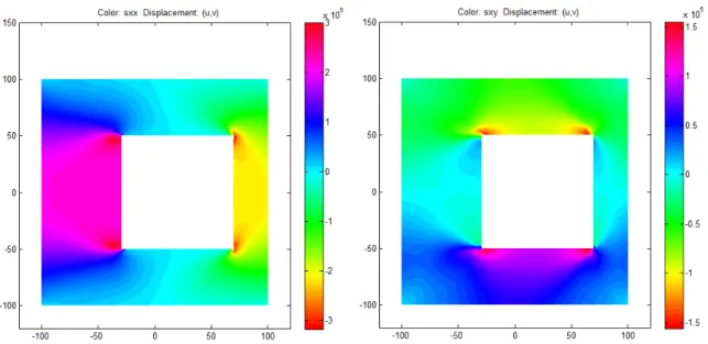
Figure
![Figure 1-2: Scanning electron micrograph of nano-patterned and folded cantilevers using designed chromium / silicon nitride stress mismatch bilayers.[1]](https://thumb-eu.123doks.com/thumbv2/123doknet/13927226.450309/23.892.136.781.252.513/scanning-electron-micrograph-patterned-cantilevers-designed-chromium-mismatch.webp)
![Figure 1-4: Scanning electron micrograph of multi-segment device folded by Laplace forces.[3]](https://thumb-eu.123doks.com/thumbv2/123doknet/13927226.450309/24.892.265.654.252.543/figure-scanning-electron-micrograph-segment-device-folded-laplace.webp)
![Figure 1-6: From [5] : Electron micrographs of sections of different 3D photonic crystal structures made by colloidal particles self-assembly.](https://thumb-eu.123doks.com/thumbv2/123doknet/13927226.450309/26.892.140.780.210.595/electron-micrographs-sections-different-photonic-structures-colloidal-particles.webp)
![Figure 1-8: From [7] : Electron micrographs of sections along different planes of a photonic crystal fabricated using holographic lithography in a 10 µm film of resist.](https://thumb-eu.123doks.com/thumbv2/123doknet/13927226.450309/27.892.300.620.321.726/electron-micrographs-sections-different-photonic-fabricated-holographic-lithography.webp)
![Figure 1-9: From [8] : Three-dimensional photonic crystals fabricated by Direct Laser Writing (DLW)](https://thumb-eu.123doks.com/thumbv2/123doknet/13927226.450309/28.892.237.678.182.391/figure-dimensional-photonic-crystals-fabricated-direct-laser-writing.webp)
![Figure 1-11: From [10] : layer-by-layer fabrication process on a single substrate show- show-ing two cycles.](https://thumb-eu.123doks.com/thumbv2/123doknet/13927226.450309/30.892.214.696.211.676/figure-layer-layer-fabrication-process-single-substrate-cycles.webp)
![Figure 1-13: From [11] : Electron micrographs of air-bridge photonic plates to be detached and stacked to form a three-dimensional photonic crystal.](https://thumb-eu.123doks.com/thumbv2/123doknet/13927226.450309/31.892.314.605.179.547/figure-electron-micrographs-photonic-detached-stacked-dimensional-photonic.webp)
![Figure 1-21: Schematics from [17] showing the principle of electrostatic actuation of tunable gratings.](https://thumb-eu.123doks.com/thumbv2/123doknet/13927226.450309/36.892.220.701.722.1054/figure-schematics-showing-principle-electrostatic-actuation-tunable-gratings.webp)
![Figure 1-22: Scanning electron micrograph showing the type of layout of an electro- electro-static actuated tunable grating from [18].](https://thumb-eu.123doks.com/thumbv2/123doknet/13927226.450309/37.892.141.780.232.608/figure-scanning-electron-micrograph-showing-electro-electro-actuated.webp)
Documents relatifs
Keywords Nonlinear Schrödinger equation; semiclassical states; Singular potential; Vanishing poten- tial; Concentration on curves; External magnetic field; Variational
Beside the rf collapse line rf sideband lines appear in the spectra (Fig. The rf sidebands are not visible in figure 1 because the first sidebands appear outside
sphere when I goes along the path [6]. Our exact diagonalizations suggest that such a semi- classical mean field picture predicts the right variation of the spin chirality as a
We have shown that it was possible to predict the equilibrium structure induced by a magnetic field in a magnetic suspension if we introduce both the repulsive interactions between
The physical origin of all the above terms is now clear and we can successively distinguish the interaction of the magnetic moment of particle i with the external
The Vlasov kinetic approach is used to study the stability of magnetic surfaces with re- spect to spontaneous excitation of collisionless tearing perturbations within magnetopause
We investigate the sedimentation of initially packed paramagnetic particles in the presence of a homogeneous external magnetic field, in a Hele-Shaw cell filled with water. Although
[r]
![[PDF] Formation MS Word 2007 pour débutant | Cours informatique](data:image/gif;base64,R0lGODlhAQABAIAAAP///wAAACH5BAEAAAAALAAAAAABAAEAAAICRAEAOw==)