HAL Id: hal-02118940
https://hal.archives-ouvertes.fr/hal-02118940
Submitted on 3 May 2019
HAL is a multi-disciplinary open access
archive for the deposit and dissemination of
sci-entific research documents, whether they are
pub-lished or not. The documents may come from
teaching and research institutions in France or
abroad, or from public or private research centers.
L’archive ouverte pluridisciplinaire HAL, est
destinée au dépôt et à la diffusion de documents
scientifiques de niveau recherche, publiés ou non,
émanant des établissements d’enseignement et de
recherche français ou étrangers, des laboratoires
publics ou privés.
An Etching-Free Approach Toward Large-Scale
Light-Emitting Metasurfaces
Gauthier Brière, Peinan Ni, Sébastien Héron, Sebastien Chenot, Stephane
Vézian, Virginie Brandli, Benjamin Damilano, Jean-Yves Duboz, Masanobu
Iwanaga, Patrice Genevet
To cite this version:
Gauthier Brière, Peinan Ni, Sébastien Héron, Sebastien Chenot, Stephane Vézian, et al.. An
Etching-Free Approach Toward Large-Scale Light-Emitting Metasurfaces. Advanced Optical Materials, Wiley,
2019, 7 (14), pp.1801271. �10.1002/adom.201801271�. �hal-02118940�
www.advopticalmat.de
An Etching-Free Approach Toward Large-Scale
Light-Emitting Metasurfaces
Gauthier Brière, Peinan Ni, Sébastien Héron, Sébastien Chenot, Stéphane Vézian,
Virginie Brändli, Benjamin Damilano, Jean-Yves Duboz, Masanobu Iwanaga,
and Patrice Genevet*
DOI: 10.1002/adom.201801271
These metasurfaces shape the wavefront by controlling its propagation with local subwavelength phase discontinuities.[4]
From the earliest experiments, associated to the reflection of light on arrays of sub-wavelength metallic patches,[5–7] the
con-cept of metasurfaces has rapidly evolved. It started from metallic metasurfaces working at a single wavelength to get to subwavelength high contrast gratings[8–11]
and even subwavelength antenna arrays of various shapes and materials working over a large bandwidth.[12–18] Today, a
broad operation wavelength range is acces-sible, going from THz down to the visible. Thanks to their reduced thicknesses and high transmission in the visible, the latest metasurface components could enable the next generation of flat optical devices. Large variety of examples of flat and small area components related to dielectric metasurfaces can be found in literature, showing impressive performances and unexpected effects, such as high transmis-sion lenses with high numerical aperture (NA), polarization controlled properties and multiplexed optical information.[19–29]
Until recently, metasurfaces have exclusively been considered as passive devices, i.e., their optical properties such as phase, amplitude and polarization responses were considered as fixed with respect to any change of environmental parameters. Their functionalities can be further expanded to a larger extent by designing tunable metasurfaces. Several attempts to achieve this tunability and switching have already been proposed, see for example the modification of the reflectivity and transmis-sion through metasurfaces fabricated from or on the top of phase change materials such as vanadium dioxide,[30–33]
chal-cogenides based on germanium antimony telluride[34–36] and
liquid crystals.[37–39] Going beyond the proof of principle of new
functionalities and practically implementing these pioneering passive and active devices necessitates new materials, enabling reduced fabrication cost, increased productivity and even higher optical performances. On the other hand, nanofabrication of metasurfaces usually involves several processing steps such as dry etching that induce unavoidable defects degrading the device optical properties and performance.
Gallium nitride, an already widespread semiconductor, is selected for the realization of our components, as it offers
A new class of quasi 2D optical components, known as metasurfaces and
exhibiting exceptional optical properties have emerged in recent years. The
scattering properties of their subwavelength patterns allow molding the
wavefront of light in almost any desired manner. While the proof of principle is
demonstrated by various approaches, only a handful of low cost and fabrication
friendly materials are suitable for practical implementations. To further develop
this technology toward broadband application and industrial production, new
materials and new fabrication methods are required. In addition, moving from
passive to active devices with, for instance, dynamic tuning requires to move
from dielectrics to semiconductors. Here, an etching-free process is presented
that combines nanoimprint and selective area sublimation of a semiconductor
material to realize centimeter-scale metalenses of high optical quality. Use of
gallium nitride is chosen for this demonstration, as it is a widespread
semi-conductor which can be transparent and active in the visible. The sublimation
leads to reduced surface roughness and defects compared to reactive ion
etching. As a result, the devices show enhanced photoluminescence efficiency
with respect to etched devices. Amplification due to gain in the semiconductor
based metaoptics could lead to a new type of optoelectronic devices.
G. Brière, Dr. P. Ni, Dr. S. Héron, S. Chenot, Dr. S. Vézian, V. Brändli, Dr. B. Damilano, Dr. J.-Y. Duboz, Dr. P. Genevet
Université Côte d’Azur
CNRS, CRHEA, Rue B. Gregory 06560, France E-mail: [email protected]
Dr. M. Iwanaga
National Institute for Materials Science (NIMS) 1-1 Namiki, Tsukuba 305-0044, Japan
The ORCID identification number(s) for the author(s) of this article can be found under https://doi.org/10.1002/adom.201801271.
Metasurfaces
1. Introduction
The most intuitive way to manipulate light relies on using clas-sical optical elements such as lenses and mirrors. For a few years, 2D optical components, also known as optical metasurfaces, have offered unprecedented possibilities to engineer light.[1–3]
© 2019 The Authors. Published by WILEY-VCH Verlag GmbH & Co. KGaA, Weinheim. This is an open access article under the terms of the Creative Commons Attribution-NonCommercial-NoDerivs License, which permits use and distribution in any medium, provided the original work is properly cited, the use is non-commercial and no modifications or adaptations are made.
www.advancedsciencenews.com www.advopticalmat.de
several advantages: a) it remains highly transparent in the entire visible range; b) its sufficiently high refractive index (e.g.,>2) ensures that GaN nanostructures exhibit strong Mie scattering resonances;[40] c) its very high thermal and chemical stability
make this material suitable even for extreme application; d) it is a very mature material, highly compatible with the semi-conductor fabrication techniques, with widespread applica-tions in electronics and optoelectronics. Pioneering works on the design[41] and the experimental realization of GaN beam
deflectors and broadband metalenses in the visible wavelength range[15,42,43] have recently been reported. For instance,
metas-urface components placed on the top of commercial LEDs have improved their extraction efficiency and controlled the degree of linear polarization of spontaneous emission.[44] With respect
to dielectric material, semiconductors have a unique advan-tage since one can realize active devices by directly embedding amplification functionality at the level of the nanopatterning. As an example, a very recent work demonstrates directional lasing from semiconductor nanoantenna based metasur-faces.[45] The low gain in nanostructured GaAs pillars,
stem-ming from its high nonradiative recombination surface states caused by the dry-etching process, limits laser operation to cry-ogenic temperatures.
In this work, experimental realization of large area, cen-timeter-scale, gallium nitride (GaN) metalenses is performed thanks to an innovative etching-free fabrication technique. This approach combines nanoimprint
lithog-raphy[46] and selective area sublimation for
high throughput, high resolution and to avoid irreversible damage caused by ion bombard-ment. Our large-area fabrication technique maintains the high material qualities after nanoprocessing and could meet the stringent requirements of industrial manufacturing processes. To further deploy metasurface technology toward dynamic applications, etching-free nanostructuration methods that would be compatible with the fabrication of large area metadevices are required. It is important to mention that the high yield fabrication of large area metasurfaces is a current objective of the community, as dis-cussed in the recent work on amorphous sil-icon metalenses fabricated using i-line deep ultraviolet (UV) stepper.[47] To address these
questions, this work establishes a basis of an innovative etching-free approach, for mass production and high yield nanofabrication of semiconductor metasurfaces that could exhibit improved optical gain. It combines the well-known nanoimprint technique with a recently developed nanostructuration tech-nique of crystalline materials called selective area sublimation (SAS).[48] By comparing
the optical performance of centimeter-scale GaN SAS metalenses with those realized with conventional dry etching methods, we demonstrate that our SAS technique gives a better control on the nanopillar morphology
leading to a higher optical quality and improved light emitting performance. Indeed, strong discrepancies in the GaN band-edge photoluminescence emission of SAS versus RIE etched devices are clearly observed, indicating the superiority of the SAS method over dry etching for the realization of active/ amplifying metasurfaces.
2. Results and Discussion
Figure 1 shows the macroscopic images and SEM pictures of the large scale metalenses fabricated by RIE and SAS, respectively. For metalenses fabricated using the RIE method, we observe that the nanopillars are highly tapered. As a contrast, the nano-pillars defined by the SAS method show much better morpholo-gies with round surface and vertical side walls. SAS respects the vertical side-wall morphology of nanopillars by taking advantage of the anisotropy of the crystalline materials during the evapora-tion process. Wurtzite GaN for example, evaporates more effi-ciently in horizontal planes (c-plane orientation) compared to stable {1100} lateral facets, leading to the well-defined nanopil-lars. Although the dry etching is compatible with both amor-phous and crystalline materials, it does not lead to a control of the nanostructure morphology as accurate as the SAS method does. The difference in the pillar morphology originates from the different fabrication processes, creating atomic scale surface
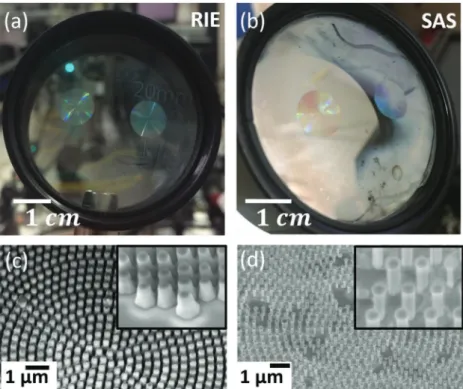
Figure 1. Comparison of the scanning electron microscopy (SEM) images of SAS and RIE
meta lenses. a–d) Macroscopic images and SEM pictures of the large-scale metalens fabricated by RIE (a,c) and SAS (b,d). Both lenses were fabricated on 2” sapphire wafer. The substrate in (a) is fully transparent while (b) shows a residual GaN layer on the edge of the metalenses due to incomplete GaN evaporation outside of the region of interest. Homogenization of tempera-ture distribution is needed to pattern full 2” inch wafers. In (c), RIE fabricated nanopillars have a tapered shape while SAS can create perfectly vertical side walls. Note the presence of missing elements in d), due to imperfect nanoimprint, and the residual ≈20 nm-thin SiN cap layer on the top of the pillars, which might affect the optical performance.
roughness in RIE etched pillars with respect to crystalline and defect-free edges obtained with SAS.
The performance of the metalenses with high numerical aperture (up to NA = 0.7) fabricated by the two methods is characterized in the ultraviolet wavelength range using a designed transmission set-up, as shown in Figure 2a. We define the transmission efficiency of the metalens as ηt = Pt/Pi, where
Pi is the optical power of the incident light, and Pt is the optical
power immediately transmitted through the metalens. By this definition, our transmission efficiency accounts for both the reflection losses at the first (air/sapphire) and metalens inter-faces, and the absorption loss. The focusing efficiency (ηf) is
defined as the optical power effectively focused by the devices, defined by the ratio of the focal spot power (Pf) to the total input
power, and is given by ηf = Pf/Pi. It is obtained by measuring the
focused light in the focal plane, by placing an aperture in the metalens focal plane before measuring the transmitted power. The transmission measurements as a function of the incident wavelength for SAS and RIE metalenses show similar trans-mission efficiencies of 37% and 43% respectively at designed wavelength of 400 nm (Figure 2c). Due to fabrication imper-fections discussed in details in the following, the transmis-sion efficiencies of both devices are lower than the numerical predictions in Figure 3d. Because SAS fabrication process respects the nanopillar vertical shape and is therefore closer than the numerically designed elements compared with the RIE method, the focusing efficiency of the SAS metalens (16%) is twice higher than the one of the RIE metalens (8%) at the
designed wavelength (Figure 2b). It is interesting to note that the power after the lens, given by ηf/ηt is above 43% for SAS
lens and 18% for the RIE lens. As shown in the SEM image in Figure 1 and in Section S2 (Figure S2, Supporting Information), under-etching effects are more important using SAS method in comparison to the RIE etching process. SAS metalenses have missing elements, creating voids that reduce the overall per-formance of the components. SAS relies on selective atomic evaporation and requires crystalline material with homoge-neous material quality, which indicates that several factors can be improved to better control the SAS process. First, the quality of the SiN mask, which is used to selectively define the area for evaporation, can be improved. Second, SAS is also sensitive to presence of dislocations in the GaN layer, which locally modify the evaporation process in the vicinity of the dislocation. We believe for example that other materials with significantly lower dislocation densities such as GaAs or other III-V compounds could improve the yield of this technique. Finally, the homoge-neity of the thermal distribution during the sublimation pro-cess is also an important factor which could be better controlled to avoid inhomogeneity. Higher focusing efficiency for SAS lenses is attributed to the better shape of the GaN nanorods in the SAS process. Unlike the total transmission, the focused power is lowered in the presence of diffused background signal, i.e., high diffracted spatial frequencies, thus indicating that the latter is more sensitive to the pillar defects. Hence, the focused power is a sensitive and pertinent probe of the optical quality of the metasurface. As discussed in Section S3 in the Supporting
Figure 2. Experimental characterization setup and efficiencies. a) Set up for measuring the efficiency. It consists of a commercial supercontinuum pulsed
laser, doubled in a nonlinear crystal to reach UV wavelengths. The light is collimated and directed onto the metalens at normal incidence. The transmitted signal is collected with a high NA objective microscope and directed to a CCD and a power meter. b) Focusing efficiency defined by the ratio of the focal spot power passing through a pinhole placed in the focal plane to the total input power and c) total transmission of the metalens as a function of the incident wavelength. Note that the GaN is absorbing below 365 nm, resulting in poor metalens focusing and transmission above bandgap energies.
www.advancedsciencenews.com www.advopticalmat.de
Information, the difference in terms of transmission amplitude and phase delays have been calculated. The data show that the increment of phase variation as a function of diameter vary dif-ferently for straight versus tapered elements. Since, the lens designs have been realized considering straight pillars, the focusing performance of SAS lenses are expected to be higher than tapered devices, as confirmed by experiments in Figure 2 and Figure S5 (Supporting Information). In Figure 4, the dis-persion behaviors of both lenses are also studied, revealing that both lenses have a similar linear dispersion in agreement with the previously reported dispersion properties of mono-chromatic metalenses.[49] Compared with dielectric materials,
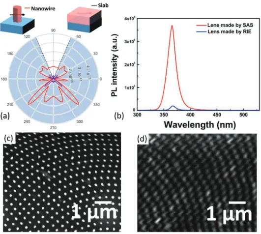
semiconductors have the unique advantage of being able to provide optical gain inside the metasurface, which opens up the possibility of realizing active metasurface based devices. It is therefore interesting to point out the difference of both devices in the passive versus active/light emitting regimes, where the etching method could drastically influence the antenna opto-electronic performances. For light emitting semiconductors, the nanostructured patterning helps to increase the extraction and even the emission efficiency (Purcell effect) of the spon-taneous emission. As confirmed in Figure 5a, the nanopillars show stronger dipole emissions than its slab counterpart. The combination of directionality and enhanced emission results from the nanopillar resonant behavior which is controlled by its geometries. However, there have been numerous reports on the irreversible damage caused by the dry etching, inducing
nonradiative carrier recombination due to the creation of vacancy-related defects at the material surfaces.[50–54] For
nanometer-scale pillars, i.e., pillars with diameters compa-rable or smaller than the carrier diffusion length, nonradiative states become dominant, and can quench the luminescence. In comparison, the SAS leads to smoother and less defective surfaces which are expected to minimize these nonradiative recombinations. This is demonstrated by comparing the room-temperature photoluminescence properties of both RIE and SAS fabricated metalenses, as shown in Figure 5b. We have conducted two photoluminescence experiments to confirm the reported results: The first setup utilize a 355-nm large Gaussian beam obtained from a passively Q-switched laser (MicroChip teemphotonics, 1 µJMax., 1 kHz rep. rate, 350 ps pulse dura-tion). The spectral emissions are collected by a 100x objec-tive, and analyzed by an Andor Shamrock 500i spectrograph (500 mm focal distance) equipped with an intensified Istar CDD camera. In the second setup, we used instead a 244 nm CW laser to confirm the results in Figure 5b. It can be seen that the photoluminescence of the SAS metalens is about two orders of magnitude higher than the one of the RIE metalens. Further-more, strong optical quality differences of the metalens are also revealed by the cathodoluminescence (CL) images, as respec-tively shown in Figure 5c,d. The CL images were recorded around the bandgap energy of GaN at room temperature under the same conditions for both metalenses. These pictures qual-itatively show that the emissions from the SAS metalens are
Figure 3. Numerical design of metasurface phased elements. a) Schematic representation of GaN nanowires on sapphire substrate. The structural
parameters are the radius r and the height h. The height is kept constant at h = 715 nm. b,c), Maps representing the transmission (b) and the phase (c) of light transmitted through a periodic array of nanowires disposed on sapphire as a function of the incident wavelength and the radius. Light is impinging at normal incidence with a linear state of polarization. Period in both x and y direction of the unit cell is 250 nm. d) Transmission (red) and phase (black) of elements used at a wavelength of 400 nm. The insets represent the near field distribution inside the different nanopillars, showing multilongitudinal mode operations.
much stronger than that of RIE devices, further confirming the superiority of the metalens fabricated by the SAS method.
3. Conclusion
In this work, we have demonstrated an innovative etching-free approach which is also compatible with mass production and high yield manufacturing of semiconductor metasur-faces with a high optical quality. This approach combines the well-known nanoimprint technique with a recently developed
nanostructuration technique of crystalline materials called selective area sublimation (SAS). We demonstrate that this technique not only provides a better control on the nano-pillar morphology but also has the advantage of maintaining a lower nonradiative recombination on the surface than the one obtained by the conventional dry etching method. Nanopil-lars and nanowires identical to those used in this manuscript have been studied for several years already to boost the LED efficiency.[55] This first realization of active/light emitting
meta-surfaces which shows the possibility of embedding the active region directly inside the interface, could also have important
Figure 4. Focusing properties and wavelength-dependent dispersion. a–d) Intensity distribution of light at the focal distance for SAS (c,d) and RIE
(a,b) fabricated lenses. e) focal shift from the designed value for SAS and RIE lenses as a function of the incident wavelength, indicating that both devices have linear dispersion as expected for monochromatic metasurfaces.
www.advancedsciencenews.com www.advopticalmat.de
implications in modern optics for controlling the light emis-sion and amplification properties of metadevices.
4. Experimental Section
For designing a lens with focal distance f, the phase response of the interface should match the phase difference between an incident planar wavefront and the spherical wavefront responsible for focusing light at the distance f. The phase distribution follows the classical lens wavefront expression given by φ( , )x y= −2λπ
(
(f2+x2+y2)−f)
[Equation (1)],[56]where λ is the operation wavelength. Metalenses were realized by disposing GaN nanopillars along a circular pattern at positions (xi,yi)
with designed structural parameters such that their scattering phase and amplitude agree with the desired phase profile expressed in Equation (1). Amplitude and phase response are generally function of the nanopillar geometrical parameters, for example height, radii (see Figure 3a). To quantify the phase retardation of light transmitted through GaN nanowires, electromagnetic simulations of arrays of nanopillars arranged in a square lattice were performed using FDTD numerical method. We specify the dispersion of GaN thin-films grown in our laboratory (as presented in Section 1 and Figure S1 in the Supporting Information), considering perfectly matched layer (PML) conditions in the direction
of the light propagation and periodic boundary conditions along all in-plane directions. The use of the PML boundary conditions at the ±z -boundaries results in an open space simulation while in plane periodic conditions mimic a subwavelength array of identical nanoparticles. The results in Figure 3b,c present the transmission phase shift due to the propagation through nanopillars and their corresponding transmission as a function of both the incident wavelength and the nanopillar radii. It was convenient in terms of fabrication to use nanopillars of the same height, and vary the diameter only. The evolution of longitudinal resonances in the pillar induces a phase shift which can reach 2π if the pillar was high enough, as shown in Figure 3d with h = 715 nm for a working wavelength of λ = 400 nm. The transmission ranges from 50% to 80% depending on the diameter. Interestingly, the phase increases with the diameter, indicating that the effective mode index increases with the ratio GaN/air. Note that the phase delay slowly saturates for larger pillars, when diameters were large enough to confine the light inside the resonator. In this work, the metalenses were designed and fabricated to operate in the UV near the GaN bandgap energy, where their focusing properties including dispersion and efficiencies were experimentally studied. Following this methodology, large area metalenses at the operating wavelength of 400 nm, with numerical apertures of 0.7 and 0.25, and the focal length of 5.1 and 19.4 mm respectively, have been designed. The fabrication process of the metalens (details can be found in the experiments section) are illustrated in Figure 6.
Figure 5. Photoluminescence spectra of light emitting metalenses. a) Numerical study showing the effect of nanostructuring on the angular
distribu-tion of the GaN emission. Nanopillars enhance the dipole emission and the forward light extracdistribu-tion. Total internal reflecdistribu-tion angles, beyond which light is total internally reflected in the case of the slab waveguide, are represented by the dashed lines. For emitters inside the slab, the TIR restricts emission in free space for light emitted beyond the TIR angle. These simulation indicate that nanopillars outcouple more than an order of magnitude more signal. b) Room-temperature photoluminescence measurements for the RIE and SAS metalenses. c,d) Cathodoluminescence measurements of SAS and RIE metalenses in imaging mode, i.e., at the zero diffraction order, integrating signal emitted at all wavelengths. These images are qualitatively different, showing strong emission for SAS with respect to RIE lenses. Note that the shapes of nanostructures appear irregular in (c) due to the low scanning electron beam sampling resolution compared to the nanopillar diameters. In (d), the image of RIE lens taken for the exact same electron beam conditions appears slightly distorted because of strong charging effects occurring at each nanopillars.
For the fabrication of a large area metalens, a 715 nm thick GaN layer was first grown on double side polished (c-plane) sapphire substrate by Molecular Beam Epitaxy (MBE) in a RIBER system. The state of the art MBE technique can provide accurate thickness control as well as large scale uniformity, needed for large area metaoptic designs. A 50 nm thick SiN was then sputtered to act as a hard mask to pattern the GaN layer. A resist was then spin-coated onto the SiN layer for nanoimprint process. Separately, a quartz master mold of metalenses has been prepared. The patterns on the master stamp were replicated onto the resist in UV nanoimprint process, and residual thin resist was removed by O2 + N2
plasma, similarly to the previous studies.[56,57] On the clearly perforated
resist pattern, we deposited 20 nm Cr for the SAS process and 50 nm Ni for the RIE process and then conducted lift-off to reveal the metallic hard masks on the SiN layer. Then, the metalens pattern was transferred onto
the SiN layer via RIE. Etching the mask does not alter the integrity of the GaN active region underneath. To further transfer the metalens design into GaN layer, two different approaches were employed, respectively: a) using a ECR-RIE dry-etching method (Oxford system 100), as shown in Figure 6a,b using the selective area evaporation, as shown in Figure 6b. At this point, we notice that it was possible to obtain straighter pillars using other RIE etching methods such as inductively coupled plasma (ICP-RIE). The second process, using atomic evaporation, was performed inside the MBE chamber under ultra-high vacuum environment by heating the patterned substrate to about 900 °C (GaN sublimation starts around 750 °C under high vacuum). The SiN hard mask was employed to protect the patterned area from evaporation due to its higher evaporation temperature, and a thin (≈20 nm) layer would remain on the top of the nanopillars after evaporation. Meanwhile, all
Figure 6. Nanofabrication processes. Schematic process flow for the fabrication of large area GaN metalenses. After nanoimpression, 50 nm Cr
(a) and respectively Ni (b), the mask is revealed for GaN dry etching (a), and respectively. evaporation (b). The SEM images show the results of the patterned metalenses. In (a), the shape of nanopillars are tapered with a relatively small tapering angle of approximately 10°. In (b), the nanopillars have vertical side walls following the crystalline orientation of the materials. In (b), the thermal uniformity on large area lens is such that a thin 5 nm GaN residual layer might appear on the edge of the lens as seen in the SEM image.
www.advancedsciencenews.com www.advopticalmat.de
the unprotected areas will evaporate, giving rise to arrays of nanowires with different diameters defined by the size of the SiN hard mask, as shown in Figure 6b. The evaporation process stops once reaching the sapphire substrate.[48] Note that the sublimation process induces more
defects, i.e., missing nanopillars, compared with RIE etching which induces diffused light scattering and reduces the metalens performance. Further discussion regarding the characteristics of the components is available in Section S2 in the Supporting Information. To quantify the optical performance, we setup a transmission measurement composed of a commercial supercontinuum laser system (NKT Photonics). Part of the visible spectrum laser was polarization filtered and injected in a second harmonic frequency doubling nonlinear crystal to generate narrow band (10 nm) UV-blue pulses tunable from 350 to 450 nm. UV beam was enlarged and collimated to a diameter of about 1 cm and directed to the metalenses, impinging at normal incidence from the substrate side. Light scattered and transmitted through the nanopillars was collected in transmission using a sensitive UV power meter.
Supporting Information
Supporting Information is available from the Wiley Online Library or from the author.
Acknowledgements
This project has received funding from the European Research Council (ERC) under the European Union’s Horizon 2020 research and innovation programme (Grant agreement no. 639109). M.I. acknowledges JSPS KAKENHI Grant (number JP17H01066). The authors thank Jun Matsuzawa for technical assistance in UV NIL. The UV NIL was conducted at Nanofabrication platform and Namiki Foundry in NIMS.
Conflict of Interest
The authors declare no conflict of interest.
Keywords
GaN, lenses, metaoptics, metasurfaces, nanoimprint lithography, optical design and fabrication, photoluminescence, selective area sublimation
Received: September 18, 2018 Revised: March 18, 2019 Published online:
[1] P. Genevet, F. Capasso, F. Aieta, M. Khorasaninejad, R. Devlin,
Optica 2017, 1, 139.
[2] H. T. Chen, A. J. Taylor, N. Yu, Rep. Prog. Phys. 2016, 7, 076401. [3] X. Luo, Adv. Opt. Mater. 2018, 6, 1701201.
[4] N. Yu, P. Genevet, M. A. Kats, F. Aieta, J.-P. Tetienne, F. Capasso, Z. Gaburro, Science 2011, 334, 333.
[5] H. Shi, C. Wang, C. Du, X. Luo, X. Dong, H. Gao, Opt. Express 2005,
13, 6815.
[6] L. Verslegers, P. B. Catrysse, Z. Yu, J. S. White, E. S. Barnard, M. L. Brongersma, S. Fan, Nano Lett. 2008, 9, 235.
[7] W. E. Kock, Bell Syst. Tech. J. 1948, 27, 58.
[8] P. Lalanne, S. Astilean, P. Chavel, E. Cambril, H. Launois, Opt. Lett.
1998, 23, 1081.
[9] S. Vo, D. Fattal, W. V. Sorin, Z. Peng, T. Tran, M. Fiorentino, R. G. Beausoleil, IEEE Photonics Technol. Lett. 2014, 26, 13.
[10] W. Stork, N. Streibl, H. Haidner, P. Kipfer, Opt. Lett. 1991, 16, 1921.
[11] Z. Bomzon, G. Biener, V. Kleiner, E. Hasman, Opt. Lett. 2002, 27, 1141.
[12] M. Khorasaninejad, Z. Shi, A. Y. Zhu, W. T. Chen, V. Sanjeev, A. Zaidi, F. Capasso, Nano Lett. 2017, 3, 1819.
[13] S. Wang, P. C. Wu, V. C. Su, Y. C. Lai, C. H. Chu, J. W. Chen, S. H. Lu, J. Chen, B. Xu, C. H. Kuan, T. Li, S. Zhu, D. P. Tsai, Nat.
Commun. 2017, 8, 187.
[14] W. T. Chen, A. Y. Zhu, V. Sanjeev, M. Khorasaninejad, Z. Shi, E. Lee, F. Capasso, Nat. Nanotechnol. 2018, 3, 220.
[15] S. Wang, P. C. Wu, V. C. Su, Y. C. Lai, M. K. Chen, H. Y. Kuo, B. H. Chen, Y. H. Chen, T. T. Huang, J. H. Wang, R. M. Lin, C. H. Kuan, T. Li, Z. Wang, S. Zhu, D. P. Tsai, Nat. Nanotechnol.
2018, 3, 227.
[16] E. Arbabi, A. Arbabi, S. M. Kamali, Y. Horie, A. Faraon, Optica 2016,
3, 628 .
[17] F. Aieta, M. A. Kats, P. Genevet, F. Capasso, Science 2015, 347, 1342.
[18] M. Khorasaninejad, F. Aieta, P. Kanhaiya, M. A. Kats, P. Genevet, D. Rousso, F. Capasso, Nano Lett. 2015, 15, 5358.
[19] Z. Zhou, J. Li, R. Su, B. Yao, H. Fang, K. Li, T. F. Krauss, ACS
Photonics 2017, 3, 544.
[20] M. Khorasaninejad, W. T. Chen, R. C. Devlin, J. Oh, A. Y. Zhu, F. Capasso, Science 2016, 6290, 1190.
[21] R. Paniagua-Dominguez, Y. F. Yu, E. Khaidarov, S. Choi, V. Leong, R. M. Bakker, X. Liang, Y. H. Fu, V. Valuckas, L. A. Krivitsky, A. Kuznetsov, Nano Lett. 2018, 3, 2124.
[22] E. Karimi, S. A. Schulz, I. De Leon, H. Qassim, J. Upham, R. W. Boyd, Light: Sci. Appl. 2014, 3, E167.
[23] G. Zheng, H. Mühlenbernd, M. Kenney, G. Li, T. Zentgraf, S. Zhang,
Nat. Nanotechnol. 2015, 10, 308.
[24] A. Niv, G. Biener, V. Kleiner, E. Hasman, Opt. Lett. 2004, 29, 238. [25] L. Huang, H. Mühlenbernd, X. Li, X. Song, B. Bai, Y. Wang,
T. Zentgraf, Adv. Mater. 2015, 27, 6444.
[26] Q. He, S. Sun, S. Xiao, Z. Lei, Adv. Opt. Mater. 2018, 6, 1800415. [27] H. Liang, Q. Lin, X. Xie, Q. Sun, Y. Wang, L. Zhou, L. Liu, X. Yu,
J. Zhou, T. F. Krauss, J. Li, Nano Lett. 2018, 18, 4460.
[28] W. T. Chen, A. Y. Zhu, M. Khorasaninejad, Z. Shi, V. Sanjeev, F. Capasso, Nano Lett. 2017, 17, 3188.
[29] W. Ye, F. Zeuner, X. Li, B. Reineke, S. He, C.-W. Qiu, J. Liu, Y. Wang, S. Zhang, T. Zentgraf, Nat. Commun. 2016, 7, 11930.
[30] M. A. Kats, R. Blanchard, P. Genevet, Z. Yang, M. M. Qazilbash, D. N. Basov, S. Ramanathan, F. Capasso, Opt. Lett. 2013, 38, 368.
[31] M. J. Dicken, K. Aydin, I. M. Pryce, L. A. Sweatlock, E. M. Boyd, S. Walavalkar, J. Ma, H. A. Atwater, Opt. Express 2009, 17, 18330. [32] D. Y. Lei, K. Appavoo, F. Ligmajer, Y. Sonnefraud, R. F. Haglund Jr.,
S. A. Maier, ACS Photonics 2015, 2, 1306.
[33] J. Rensberg, S. Zhang, Y. Zhou, A. S. McLeod, C. Schwarz, M. Goldflam, M. Liu, J. Kerbusch, R. Nawrodt, S. Ramanathan, D. N. Basov, F. Capasso, C. Ronning, M. A. Kats, Nano Lett. 2016,
16, 1050.
[34] A. Karvounis, B. Gholipour, K. F. MacDonald, N. I. Zheludev, Appl.
Phys. Lett. 2016, 109, 051103.
[35] Q. Wang, E. T. F. Rogers, B. Gholipour, C. M. Wang, G. Yuan, J. Teng, N. I. Zheludev, Nat. Photonics 2016, 10, 60.
[36] C. H. Chu, M. L. Tseng, J. Chen, P. C. Wu, Y. H. Chen, H. C. Wang, T. Y. Chen, W. T. Hsieh, H. J. Wu, G. Sun, D. P. Tsai, Laser Photonics
Rev. 2016, 1.
[37] M. Decker, C. Kremers, A. Minovich, I. Staude, A. E. Miroshnichenko, D. Chigrin, D. N. Neshev, C. Jagadish, Y. S. Kivshar, Opt. Express 2013, 21, 8879.
[38] O. Buchnev, N. Podoliak, M. Kaczmarek, N. I. Zheludev, V. A. Fedotov, Adv. Opt. Mater. 2015, 3, 674.
[39] B. Kang, J. H. Woo, E. Choi, H.-H. Lee, E. S. Kim, J. Kim, T. J. Hwang, Y. S. Park, D. H. Kim, J. W. Wu, Opt. Express 2010, 18, 16492.
[40] Y. Feng Yu, A. Y. Zhu, R. Paniagua-Dominguez, Y. H. Fu, B. Luk’yanchuk, A. I. Kuznetsov, Adv. Opt. Mater. 2015, 3, 813. [41] Z. Guo, H. Xu, K. Guo, F. Shen, H. Zhou, Q. Zhou, J. Gao, Z. Yin,
Nanomaterials 2018, 8, 333.
[42] N. K. Emani, E. Khaidarov, R. Paniagua-Domínguez, Y. H. Fu, V. Valuckas, S. Lu, X. Zhang, S. T. Tan, H. V. Demir, A. I. Kuznetsov,
Appl. Phys. Lett. 2017, 111, 221101.
[43] B. H. Chen, P. C. Wu, V. Su, Y. C. Lai, C. H. Chu, I. C. Lee, J. W. Chen, Y. H. Chen, Y. C. Lan, C. H. Kuan, D. P. Tsai, Nano Lett.
2017, 17, 6345.
[44] M. Wang, F. Xu, Y. Lin, B. Cao, L. Chen, C. Wang, J. Wangc, K. Xu,
Nanoscale 2017, 9, 9104.
[45] S. T. Ha, Y. H. Fu, N. K. Emani, Z. Pan, R. M. Bakker, R. Paniagua-Dominguez, A. Kuznetsov, Nat. Nanotechnol. 2018, 13, 1042.
[46] Y. Yao, W. Wu, Adv. Opt. Mater. 2017, 1002, 1700090.
[47] A. She, S. Zhang, S. Shian, D. R. Clarke, F. Capasso, Opt. Express
2018, 22, 1573.
[48] B. Damilano, S. Vézian, J. Brault, B. Alloing, J. Massies, Nano Lett.
2016, 16, 1863.
[49] F. Aieta, P. Genevet, M. A. Kats, N. Yu, R. Blanchard, Z. Gaburro, F. Capasso, Nano Lett. 2012, 12, 4932.
[50] H. K. Cho, F. A. Khan, I. Adesida, Z.-Q. Fang, D. C. Look, J. Phys. D:
Appl. Phys. 2008, 41, 155314.
[51] Z. Mouffak, A. Bensaoula, L. Trombetta, J. Semicond. 2014, 35, 113003.
[52] H. Lee, D. B. Oberman, J. S. Harris, Appl. Phys. Lett. 1995, 67, 1754.
[53] M. E. Lin, Z. F. Fan, Z. Ma, L. H. Allen, H. Morkoç, Appl. Phys. Lett.
1994, 64, 887.
[54] I. Adesida, A. Mahajan, E. Adesida, M. A. Khan, D. T. Olsen, J. N. Kuznia, Appl. Phys. Lett. 1993, 63, 2777.
[55] S. Konsek, J. Ohlsson, Y. Martynov, P. J. Hanberg, US9595649B2, USA, 07 07, 2008.
[56] B. Choi, M. Iwanaga, H. T. Miyazaki, K. Sakoda, Y. Sugimoto,
J. Micro/Nanolithogr., MEMS, MOEMS 2014, 13, 023007.