HAL Id: cea-02185285
https://hal-cea.archives-ouvertes.fr/cea-02185285
Submitted on 16 Jul 2019
HAL is a multi-disciplinary open access
archive for the deposit and dissemination of
sci-entific research documents, whether they are
pub-lished or not. The documents may come from
teaching and research institutions in France or
abroad, or from public or private research centers.
L’archive ouverte pluridisciplinaire HAL, est
destinée au dépôt et à la diffusion de documents
scientifiques de niveau recherche, publiés ou non,
émanant des établissements d’enseignement et de
recherche français ou étrangers, des laboratoires
publics ou privés.
A Novel Structure for Backside Protection Against
Physical Attacks on Secure Chips or SiP
S. Borel, L. Duperrex, E. Deschaseaux, J. Charbonnier, J. Clédière, R.
Wacquez, J. Fournier, J. Souriau, Grégory Simon, A. Merle
To cite this version:
S. Borel, L. Duperrex, E. Deschaseaux, J. Charbonnier, J. Clédière, et al.. A Novel Structure for
Backside Protection Against Physical Attacks on Secure Chips or SiP. 2018 IEEE 68th Electronic
Components and Technology Conference (ECTC), May 2018, San Diego, United States. pp.515-520,
�10.1109/ECTC.2018.00081�. �cea-02185285�
A Novel Structure for Backside Protection
Against Physical Attacks on Secure Chips or SiP
S. Borel, L. Duperrex, E. Deschaseaux, J. Charbonnier, J. Cledière,
R. Wacquez, J. Fournier, J.-C. Souriau, G. Simon, A. Merle
Univ. Grenoble Alpes, CEA, LETI, 38000 Grenoble, France [email protected] ; +33 4 38 78 29 17
Abstract — A structure intended to protect Integrated Circuits (IC) against physical attacks is presented. Located on the backside of a chip, it complements the countermeasures usually available on the front side of secure components. It aims at preventing attacks such as fault injection by laser illumination and can trigger an alert in case of invasive attacks by circuit edit or micro-probing. Weakening structures have been designed so as to cause the breakage of the die in case of thinning, and a metallic serpentine used as an attack witness has been thought with a maximal complexity so that an attacker cannot skirt it. These elements can be fabricated using standard packaging techniques in a wafer level integration, whether at chip or system scale. The concept of a secure System in Package (SiP) using unsecured chips is proposed, opening the perspective of components fully “secured by packaging”.
Keywords - cybersecurity; backside; 3D integration; wafer level packaging; secure SiP
I. INTRODUCTION
Security and privacy are jeopardized by the growing use of electronic devices that manage, store and share personal or confidential data [1]. Cybersecurity is a key point and will become a real challenge in the coming years since the number of connected objects is increasing at a vertiginous rate [2]. The Internet of Things (IoT) covers a wide range of objects going from non-critical ones such as smart toothbrushes to more sensitive ones like banking terminals or medical devices (pacemakers, glucose meters, drug pumps, imaging tools) [3]. The respect of privacy and confidentiality within these devices is necessary for their adoption by the general public, but at a higher level also, it is mandatory to take all precautions to ensure that a hospital or a military facility cannot be hacked because of a lack of security in their network or among the mobile devices that communicate with it [4].
Secure IC are usually designed to withstand attacks aiming for example to retrieve a secret key by physical means such as fault injection [5] or micro-probing [6]. Countermeasures implemented in their technology shall prevent hackers from accessing or modifying their constituents; they shall also trigger an alert in case of intrusion so that the IC can take appropriate actions to protect the sensitive information [7]. Due to these protections, hackers have developed techniques to access the active parts of the IC from the backside of the chips [8].
Infrared (IR) lasers can be used through the substrate to inject faults in the IC since silicon is transparent for these wavelengths. The circuit’s reaction to these faults may acquaint the hacker with normally inaccessible information [9]. Moreover, a Focused Ion Beam (FIB) allows to dig cavities from the backside to probe active zones or metal lines that are shielded from the opposite side, with the aim of observing signals [10]. In this context, backside protections are under development to complement those located on the front side but their maturity is not comparable and their deployment remains anecdotic [11].
In a previous work [12] we described a backside protection based on several elements that we fabricated using packaging techniques. This concept proved to be efficient against physical attacks such as fault injection or FIB edit, but the structure remained intelligible by a hacker due to layout considerations so it required some improvements. This work has been pursued by exploring new designs, fabrication processes and integration schemes in order to propose a more robust protection.
In the next section we present our concept of backside protection by describing the structure we first developed and evaluated. In the following section, we introduce some new features to make the shield more customizable and above all more difficult to analyze and attack. In the last section we propose an integration scheme to implement these countermeasures on the backside of a chip or to make a secure SiP.
II. BACKSIDE PROTECTION CONCEPT
A. Initial Structure
Our backside shield (Fig. 1) includes blind holes that are deeply etched in the silicon substrate and lined with a metal layer. Their function is to weaken the chip and lead to its physical breakage in case of a mechanical stress induced by an attack by micro-milling for example. Since the metal layer is opaque to IR, the cavities also constitute a 3D shield which prevents fault injection by laser illumination.
Through Silicon Vias (TSV) are fabricated simultaneously in a via last approach, the metal liner inside the blind cavities serving as a seed layer for the thick copper electroplating in the TSV. In the first version, these TSV had a diameter of 70µm for a depth of 180µm.
After corking the open cavities with polymer, a metallic serpentine is realized and connected to the IC using the TSV. It is used as an attack witness since any damage caused by an
Figure 1. Cross-sectionnal schematic view of the structure initially developed for backside protection.
attack results in a modification of its electrical resistance which can be detected by the IC. In the initial structure, a 2D serpentine made of 10µm/10µm (line/space) patterns was realized in a 2µm-thick AlSi layer and showed a resistance of 1.4 kȍ for a 3.5x3.5 mm² area.
Finally, a black polymer film laminated over the structure prevents from observing the underlying patterns and constitutes an additional shield against lasers since this molding compound (epoxy matrix with glass fillers) showed to be opaque in the visible and near-IR range (Fig. 2). Indeed, a transmission of 0.02% was measured at 1064 nm which is a typical wavelength for fault injection, and the value barely exceeded 0.2% in the explored range (400 < λ(nm) < 2400). The forward power required to generate a photo-current in an active area located beyond the polymer would thus be unreachable, all the more so since the metal parts underneath are also contributing to the shielding effect.
Figure 2. Transmission spectrum of a 120µm-thick sheet of molding polymer in the visible and near-IR range.
Moreover, this polymer represents a good protection against FIB as it causes a beam deflection due to charges accumulation on the treated surface, which disturbs the precise positioning of the ablation window.
Finally, it is more resistant to chemicals such as nitric acid than the one used to cork the cavities, thus its removal is very tricky without cutting the serpentine and triggering an alert.
B. Limitations of the initial structure
In their first version, the blind structures were circular holes of various diameters ranging from 10 to 40µm so that their depths were lower than that of the TSV (70µm in diameter) due to the Aspect Ratio Dependent Etching (ARDE) effect [13] as shown on Fig. 3b.
(a) (b)
Figure 3. (a) Top view of the TSV and blind cavities after lithography and (b) their depth after deep etching (measured by Scanning Electron
Microscopy).
As a consequence, it was (theoretically) possible for a hacker to locate the extremities of the serpentine by identifying the TSV thanks to their higher diameter, then to connect a resistor with the same characteristics so as to subsequently be able to cut the serpentine without triggering an alert. Nevertheless this procedure is very challenging since the encapsulating polymer prevents from analyzing the patterns underneath and cannot be removed easily without also removing the underlying polymer or damaging the serpentine, leading to its modification in both cases.
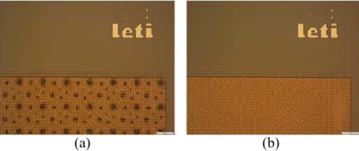
Another limitation of the initial structure was the serpentine’s design. A single level integration was implemented first in order to evaluate the concept, but the complexity with a 2D serpentine was limited, even if the design looked very winding (Fig. 4) and was hidden by the thick and opaque molding polymer.
(a) (b)
Figure 4. Top view micrograph of an AlSi serpentine patterned on top of a metallic shield with (a) or without (b) weakening structures.
Furthermore, the dependence of the serpentine’s resistance with temperature was a source of misinterpretation by the IC. Indeed, the detection threshold to trigger an alert must be higher than the variations due to external parameters such as temperature in order to avoid false positives. Depending on the operating temperature range, these values may be significant. Fig. 5 shows the average resistance of AlSi serpentines as a function of temperature ranging from -40°C to 120°C. Within this range, the resistance varies from -22% to +28% as compared to the value at 20°C. A 30% threshold may not be suitable for a fine detection. Nevertheless, during the first evaluation of our structure, an increase of the resistance as high as 60% was caused by a tungsten patch on the serpentine [12].
Figure 5. Electrical resistance (normalized to 20°C) as a function of temperature for AlSi serpentines.
III. NEW IMPLEMENTATIONS
A. Weakening structures
The weakening structures are critical elements since their role is to increase the fragility of the chips so that they break in case of attack, but they must not cause any breakage during the fabrication process or under normal conditions of use. In order to optimize their shape, size and density we carried out a mechanical study based on Finite Elements (FE) Simulation in association with bending tests. For these tests we chose a Ball on Ring (BoR) configuration [14], [15] which avoids taking into account the quality of the sample edges and its effect on the breakage force.
A ball with a diameter of 1mm was used to stress the backside of the samples in a region located at the center of a ring with an internal diameter of 3mm. The force vs. displacement curves were plotted using a Shimadzu EZ-SX tester and the breakage force was recorded at 5 different stages of the backside process and for 3 different variants of patterns (Fig. 6):
- no blind hole
- blind holes with a density of 200/mm² - blind holes with a density of 450/mm²
Figure 6. Breakage force measured for 3 different pattern densities: 0 (in blue); 200 (in red); 450 (in green) holes/mm².
These values show that the presence of blind holes is indeed weakening the chips, all the more so when their density increases: the average breakage force on thinned samples was around 18N and it decreased to 16N (resp. 12N) for the lower (resp. higher) holes density just after etching. The fragility changed throughout the process but it is
important to note that at the end (after encapsulation with the molding polymer) the chips were stronger (breakage force of 23N for both densities) than ones with no backside shield. This complies with the need for a mechanical strength under normal conditions of use and a fragility in case of attack.
Some samples were measured on the BoR tester by stressing their front side so as to generate cracks on their backside. They were then observed on a microscope in order to determine the starting point of the cracks as well as their propagation directions. In most cases the cracks were initiated on a same pattern consisting of a small hole (10µm in diameter) located close to another (bigger) one. In order to formalize these observations, the structure with our arbitrary holes distribution was modeled and a FE method was used to simulate the bending of a chip with weakening structures in a BoR configuration so as to reproduce our experimental conditions (Fig. 7).
Figure 7. FE simulation of a silicon chip (half-sample in blue) bent in a BoR configuration.
The simulation indicated this precise location as the maximum of tensile stress on backside (Fig. 8), highlighting the influence of both the diameter and the density of the blind holes.
Figure 8. Good correlation between the maximum of stress obtained by simulation (center) and the observed starting points of cracks after a BoR
solicitation (left and right).
Since small diameters correspond to shallow holes, the most influencing structures are eliminated first in case of thinning from the backside, which is not desirable. For that reason, we propose a new shape for the weakening structures so as to de-correlate their depth and stress concentration. Instead of circular holes of which surface is determined by their diameter, some round-corner squares were simulated in the BoR configuration with different surfaces (determined by their side) and different radius of curvature in their angles, these patterns being repeated with different densities. The conclusion was that the surface and density of the pattern mainly influence the rigidity of the die whereas the radius of curvature determines its fragility. So in case of precise specifications on rigidity and fragility, for a given pattern surface deducted from the target depth, the density and the
radius of curvature in the angles can be tuned so as to reach the desired values. In our case, they were sized to offer the same performances as the highest density of first generation patterns. Their dimensions are given below:
- side = 55µm
- radius of curvature = 5µm
- pitch = 200µm in both x and y directions
These patterns were etched on thinned samples, then BoR measurements were done to confirm the breakage force, but their final shape was modified (see next section) which slightly shifted the samples’ rigidity as compared to the first generation patterns.
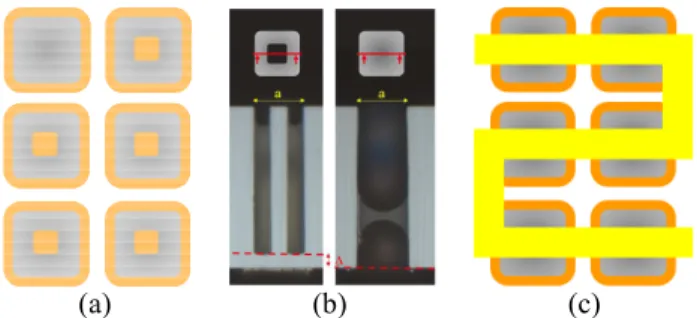
B. Indistinguishable TSV
The possibility for a hacker to locate the TSV has been a motivation to rethink them in the light of the new shape proposed for the weakening structures. The challenge was to realize blind holes and through holes simultaneously (meaning with no additional process step) in a manner that makes the TSV undistinguishable from the weakening structures. For that we proposed to design both types of holes with the same external dimensions and to add a pillar in the middle of the weakening structures (Fig. 9a) so as to reduce their depth after deep etching due to a smaller open area (or a higher Aspect Ratio (AR)) (Fig. 9b). These pillars are then covered with the serpentine so as to be invisible in the final structure (Fig. 9c). In that aim, a matrix distribution of the weakening holes (with TSV among them) is preferable so that the serpentine can cover them while keeping an almost regular design.
The simulation of this innovative structure showed no modification of the fragility due to the presence of the pillar that only changes the surface so the rigidity. The etching process was developed using a mask with different pillar dimensions so as to determine the right AR to get blind holes with the right depth. It was validated on 55µm squares with pillars of side a=20µm. In this configuration, the differential depth, compared with empty holes intended for TSV, was Δ=20µm as desired (Fig. 9b).
(a) (b) (c)
Figure 9. Weakening structures and TSV designed identically apart from pillars (a)(b) that are finally hidden by the serpentine (c).
In the initial configuration, only the TSV were metallized with a thick electroplated copper whereas the blind holes were just lined with the seed layer serving as a 3D metallic shield. In this new approach, the blind holes must be metallized together with the TSV so as to look similar when viewed from above. This metallization requires a specific
development due to the presence of the pillars that increase the AR in the weakening holes. However these structures have no electrical function so the metal thickness and quality at their bottom is not critical. The only requirement relates to the opacity to IR but previous measurements [12] showed that it was provided by the seed layer which is conformal due to the CVD process used for its deposition.
C. Multilayer serpentines
The control of a serpentine’s resistance in order to detect any change imputable to an attack implies storing a reference value in a memory so as to evaluate whether or not a variation is significant and should trigger an alert. In our novel structure, the serpentine is doubled so that the IC compares the resistance of both parts, with no need for a reference value and no impact of the natural variations such as thermal ones. The two parts of the serpentine must be different and very hard to analyze so that an attacker cannot simply apply the same modification on both of them to mislead the control. In that aim, an improvement consisted in adding a level to the serpentine technology, at no extra cost, meaning no additional mask or process step. For that we proposed to use the TSV metallization (electroplated copper) for the lower serpentine level (Fig. 10b) which implies patterning the seed layer instead of keeping it as a blanket shield (Fig. 10a).
(a) (b)
Figure 10. Comparison between the initial (a) and the novel (b) structure regarding TSV metallization. The yellow part is the seed layer, the orange
one is the electroplated copper.
The lower part of the serpentine can transit through blind holes (center of Fig. 11). This further increases the difficulty to distinguish the TSV since they are no longer the only structures connected to a serpentine.
Figure 11. Example of a (lower) serpentine going from one TSV to another through a blind cavity.
For the upper level, the same integration as in the initial structure is retained except that the corking polymer is opened in multiple vias to connect the aluminum parts (upper level) to the copper ones (lower level). This allows to drastically increase the complexity of the design since the two serpentines can be intermingled without any dead end limitation.
Figure 12. Top view (from the backside) of a protection structure with the upper part of the serpentine (in yellow) partially hiding the lower part (in
orange) as well as the TSV and weakening structures (in blue) that are indistinguishable.
Once the two levels are superimposed, the reduced visibility of the lower level makes it impossible for a hacker to distinguish the TSV and to know which parts of the traces belong to which serpentine (Fig. 12).
IV. WAFER LEVEL INTEGRATION
A. Chip scale
This novel structure, just like the previous version, can be realized at chip scale in a wafer level approach by processing wafers mounted on carriers. A permanent bonding can be used for that, but since all the processes on backside are performed at low temperature (below 200°C), temporary bonding using a thermoplastic adhesive in a slide-off or ZoneBOND® process is also feasible and was our preferred option.
The wafer level integration offers the opportunity by a single step to assign different serpentine designs to the dies across a same wafer. Indeed, the lithography steps are not critical in terms of alignment so they can be performed on a mask aligner rather than on a stepper. By doing so we were able to test different designs, and now we propose to multiply the number of designs so that each die has its own serpentine drawing. The hacker’s task is thus harder since an attack developed on a die cannot always be applied on another one even if the dies look similar and come from similar devices. Admittedly the huge work to generate unique designs for all the dies on a wafer has to be automated considering the complexity of a double serpentine realized on two levels.
At the end of the process, the dies (Fig. 13) are sawed and ready for assembly in a package or on a Printed Circuit Board (PCB) with no specific precaution related to the presence of the backside protection since their mechanical strength is even higher than that of dies with no shield on backside (Fig. 6).
Figure 13. Schematic cross-sectional view of a die with the novel structure implemented on backside.
B. System scale
The concept and the technology of this backside shield can be extended to a set of multiple dies provided that their backsides are linked in a coplanar way. We have studied the way of securing the backside of a system made of several dies, still in a wafer level approach, using a 2.5D integration (Fig. 14). An interposer with a redistribution layer (RDL) and interconnections such as bumps or pillars (a) is used to receive the different dies assembled by flip-chip (b). The dies are molded and underfilled (c) then planarized (d) so as to expose their backside. The previously described process can finally be applied on a surface corresponding to the whole system (e and f).
Figure 14. Secure SiP obtained starting from non-secured chips in a 2.5D integration.
One advantage of this approach is the possibility to make a secure SiP starting from non-secured chips. Indeed, in addition to protecting collectively the backside of the chips by realizing our shield structure, it is proposed to embed some countermeasures (CM) inside the interposer (Figure 14. a) so as to protect the front sides that are facing them. The smart interposer thus achieved can encompass anti-probing layers, photodiodes or other elements commonly found on secure devices. It could also include the logic aiming at managing the security of the system but most probably a chip dedicated to this would be designed specifically and included into the set of chips that constitute the system.
V. CONCLUSION
Secure chips can benefit from a more effective protection on their backside thanks to a novel structure that we developed using packaging techniques in a wafer level approach. Weakening holes have been designed to cause the breakage of the die in case of thinning by micro milling. Their shape, size and density have been optimized and made compatible with the simultaneous realization of TSV that cannot be distinguished in the end, making it more difficult for a hacker to skirt the serpentine used as an attack witness. This serpentine is made of two parts to be insensitive to temperature variations. It has been proposed in a two level integration so as to maximize the complexity of its design and prevent hackers from analyzing and modifying it using a FIB. The structure can be fabricated at die level on any kind of substrate (bulk, SOI) but also in a SiP configuration using a smart interposer which can contribute to the protection by embedding countermeasures. It is then possible, starting from non-secured chips, to obtain a SiP secured by the packaging.
ACKNOWLEDGMENT
The authors would like to thank Romain Anciant for the electrical tests as well as Stéphanie Anceau and Philippe Medina for the physical attacks. They are also grateful to N. Owing for his work on the automatic generation of serpentine designs.
REFERENCES
[1] S. Bhunia, S. Ray and S. Sur-Kolay, “Fundamentals of IP and SoC Security”, 2016.
[2] M. Semeria, “Symbiotic Low-Power, Smart and Secure Technologies In the Age of Hyperconnectivity”, IEEE 62nd International Electron
Devices Meeting (IEDM), 2016, pp. 9-22.
[3] K. Daniluk, E. Niewiadomska-Szynkiewicz, “Energy-Efficient Security in Implantable Medical Devices”, Federated Conference on Computer Science and Information Systems (FedCSIS), 2012, pp. 773-778.
[4] E. Ronen, C. O’Flynny, A. Shamir and A.-O. Weingarten, “IoT Goes Nuclear : Creating a ZigBee Chain Reaction”, IACR Cryptology ePrint Archive, No 1047, 2016, pp.195-212.
[5] A. Krakovinsky, M. Bocquett, R. Wacquez, J. Coignus, D. Deleruyelle, C. Djaout, G. Reimbold and J.-M. Portal, “Impact of a Laser Pulse On Hf02-based RRAM Cells Reliability and Integrity”, International Conference on Microelectronic Test Structures (ICMTS), 2016, pp. 152-156.
[6] R. Schlangen, R. Leihkauf, U. Kerst, C. Boit, and B. Kruger, ”Functional IC Analysis Through Chip Backside With Nano Scale Resolution - E-Beam Probing in FIB Trenches to STI Level”, International Symposium on the Physical and Failure Analysis of Integrated Circuits, 2007, pp. 35-38.
[7] S. Manich, M. S. Wamser, G. Sigl, “Detection of Probing Attempts in Secure ICs”, IEEE International Symposium on Hardware-Oriented Security and Trust (HOST), 2012, pp. 134-139.
[8] C. Helfmeier, D. Nedospasov, C. Tarnovsky, J. Krissler, C. Boit, and J.-P. Seifert. “Breaking and entering through the silicon”, Proc. of the 20th ACM conference on Computer and communications security, 2013, pp. 733-744.
[9] C. Boit, S. Tajik, P. Scholz, E. Amini, A. Beyreuther, H. Lohrke and J. Seifert, “From IC Debug to Hardware Security Risk: The Power of Backside Access and Optical Interaction”, IEEE 23rd Symposium on
the Physical and Failure Analysis of Integrated Circuits (IPFA), 2016, pp. 365-369.
[10] Dmitry Nedospasov, “Attacking Microchips through the Backside”, 15th PacSec Conference, 2013.
[11] S. Manich, D. Arumi, R. Rodriguez-Montanes, “Backside Polishing Detector: A New Protection Against Backside Attacks”, Conference on Design of Circuits and Integrated Systems (DCIS), 2015, pp. 1-6. [12] S. Borel, E. Deschaseaux, J. Charbonnier, Ph. Medina, S. Anceau, J.
Cledière, R. Wacquez, J. Fournier, E. Jalaguier, C. Plantier and G. Simon, “Backside Shield against Physical Attacks for Secure ICs”, Device Packaging, 2017, pp. 1-15.
[13] J. Yeom, Y. Wu and M. A. Shannon, “Critical Aspect Ratio Dependence in Deep Reactive Ion Etching of Silicon”, 12th
International Conference on Solid State Sensors, Actuators and Microsystems (Transducers), 2003, pp. 1631-1634.
[14] G. de With and H. H. M. Wagemans, “Ball-on-Ring Test Revesited”, J. Am. Ceram. Soc., Vol. 72, 1989, pp. 1538-1541.
[15] J.-H. Zhao, J. Tellkamp, V. Gupta and D. Edwards, “Experimental Evaluations of the Strength of Silicon Die by 3-Point-Bend Versus Ball-on-Ring Tests”, IEEE Trans. Electron. Packag. Manuf., Vol. 32, No. 4, 2009, pp. 248– 255.