ARCH1VES
-'I IS ErFS NSTf(]
Communication and Energy Delivery
Architectures for Personal Medical Devices
by
Patrick Philip Mercier
B.Sc. in Electrical and Computer Engineering, University of Alberta,
2006
S.M. in Electrical Engineering and Computer Science, Massachusetts
Institute of Technology, 2008
Submitted to the Department of Electrical Engineering and Computer
Science
in partial fulfillment of the requirements for the degree of
Doctor of Philosophy
at the
MASSACHUSETTS INSTITUTE OF TECHNOLOGY
June 2012
©
Massachusetts Institute of Technology 2012. All rights reserved.
Author ... ...
Department of Electrical Engineering and Computer Science
May 21, 2012
Certified by ...
Anantha P. Chandrakasan
Joseph F. and Nancy P. Keithley Professor of Electrical Engineering
Thesis Supervisor
A ccepted by...
....
...
Carlie A. Kolodziejski
Communication and Energy Delivery Architectures for
Personal Medical Devices
by
Patrick Philip Mercier
Submitted to the Department of Electrical Engineering and Computer Science on May 21, 2012, in partial fulfillment of the
requirements for the degree of Doctor of Philosophy
Abstract
Advances in sensor technologies and integrated electronics are revolutionizing how humans access and receive healthcare. However, many envisioned wearable or im-plantable systems are not deployable in practice due to high energy consumption and anatomically-limited size constraints, necessitating large form-factors for external de-vices, or eventual surgical re-implantation procedures for in-vivo applications.
Since communication and energy-management sub-systems often dominate the power budgets of personal biomedical devices, this thesis explores alternative use-cases, system architectures, and circuit solutions to reduce their energy burden. For wearable applications, a system-on-chip is designed that both communicates and de-livers power over an eTextiles network. The transmitter and receiver front-ends are at least an order of magnitude more efficient than conventional body-area networks.
For implantable applications, two separate systems are proposed that avoid re-implantation requirements. The first system extracts energy from the endocochlear potential, an electrochemical gradient found naturally within the inner-ear of mam-mals, in order to power a wireless sensor. Since extractable energy levels are limited, novel sensing, communication, and energy management solutions are proposed that leverage duty-cycling to achieve enabling power consumptions that are at least an order of magnitude lower than previous work. Clinical measurements show the first system demonstrated to sustain itself with a mammalian-generated electrochemical potential operating as the only source of energy into the system. The second sys-tem leverages the essentially unlimited number of re-charge cycles offered by ultra-capacitors. To ease patient usability, a rapid wireless capacitor charging architecture is proposed that employs a multi-tapped secondary inductive coil to provide charging times that are significantly faster than conventional approaches.
Thesis Supervisor: Anantha P. Chandrakasan
Acknowledgments
It has been quite the journey. A journey that began as a fresh incoming graduate student trying to figure out how the MIT building numbering system makes sense (hint: it doesn't). A journey that culminates in the submission of a Ph.D. thesis, but encompasses so much more than just the contents of this document. My time in graduate school has been exciting, challenging, and rewarding not only for my own professional development, but also for my own personal growth.
I've been very fortunate to have a lot of help and inspiration to guide me along the way. I am indebted to my advisor, Anantha Chandrakasan, for providing me with the inspiration to push the boundaries of research and state-of-the-art design. Your advice, not only on technical issues, but also on topics of funding, industry relations, organization, and logistics have been invaluable. You have taught me that a successful researcher is not only inventive and thoughtful, but also sincere, cooperative, and respectful (and generously cites the work of others!). I would also like to extend my sincerest gratitude to my Ph.D. thesis committee members for all their contributions and support: Joel Dawson, Konstantina (Tina) Stankovic, and Charlie Sodini. I would especially like to thank Tina for the exciting energy, ideas, and clinical expertise
brought into the inner-ear related work.
Naturally, none of this work could have been accomplished without the generous support of funding partners. I would like to thank Intel Corporation, the Center for Circuit and System Solutions (C2S2), the Interconnect Focus Center (IFC), and the Natural Sciences and Engineering Research Council of Canada (NSERC) for providing me with fellowship, assistantship, and scholarship support.
I often get asked what the best thing about MIT is. I've come to learn that the answer is incredibly easy - it's the people. It's not the buildings, the infrastructure, the equipment, or the location that makes MIT such a great place to learn and discover - it's the people in the MIT community. Faculty members and visiting scientists such as Vladimir Stojanovic, Dina Katabi, Muriel Medard, Dana Weinstein, and Dennis Buss have taught me that collaborations across various disciplines and industries can
lead to powerful concepts and results. Student collaborators are equally important - I would like to acknowledge Saurav Bandyopadhyay for co-designing the energy harvesting chip, and Andrew Lysaght for performing guinea pig surgeries. We spent many long hours in that hot chamber, but the results were certainly worth it! I'd like to thank Phillip Nadeau and Arun Paidimarri for the invigorating discussions on RF circuits and successful implementations of multi-channel FBAR-based radios - it has been a pleasure working with you and I learned a lot throughout the process. Tapeouts can always be difficult, especially with a new PDK - working in parallel with Jose Bohorquez and Marcus Yip made this process much more bearable. I'd also like to acknowledge Sushmit Goswami and Benjamin Tay for valuable discussions and pre-initial-prototype developments of the wireless energy transfer project. Co-chairing the MTL Annual Research Conference with Priya Jadhav was a wonderful experience, and I'd like to thank the entire steering committee, especially Debb Hodges-Pabon, for all their ideas, help, and hard work.
I've had the luxury of sharing my time here with many other incredibly insightful and fun people. Michael Georgas - we had a great time interning in Oregon, and our recent tradition of getting coffee or lunch has been most welcome. Denis Daly - I learned an incredible amount from you as a mentor, as a friend, and as an
ice-hockey teammate. Jose Bohorquez - it's been a pleasure spending time with you and your family; your research insight and suggestions have been extremely valuable. Marcus Yip - thank you for being a great cube-mate and introducing me to some fantastic craft-brewed wheat-based beverages. To the golf crew: Fred Chen, Michael Georgas, Jose Bohorquez, David Tax, Marcus Yip, and Al Avestruz - I hope one of us finds that ever elusive hole-in-one someday! I'd also like to thank Ranko Sredojevic, Robert Pilawa, Willie Sanchez, Eric Winokur, David He, David Shirokoff, Fergus Hurley, Byungsub Kim, and many others for being wonderful friends and colleagues. Past and present members of ananthagroup have had a significant impact on my personal and professional development. I'd like to thank Manish Bhardwaj, David Wentzloff, Brian Ginsburg, Naveen Verma, Nathan Ickes, Yogesh Ramadass, Daniel Finchelstein, Joyce Kwong, Vivienne Sze, Nigel Drego, Payam Lajervardi,
Alexan-dra Kern, Jae Lee, and Chih-Chi Cheng for being excellent mentors and colleagues. Mahmut Ersin Sinangil, Masood Qazi, and I all arrived in ananthagroup at roughly the same time - it's hard to believe where the time has gone. I still vividly remember taking our first few classes together, working on projects primarily with Mahmut. It's also exciting to see the next generation of students join and continue the ex-cellent legacy of ananthagroup: Georgios, Kailian, Nachiket, Dina, Sungjae, Bonnie, Sunghyuk, Michael, Priyanka, Rahul, Yildiz, Mehul, and Frank. Margaret Flaherty most certainly an acknowledgment here for being on-top of everything and keeping
38-107 running so smoothly!
Finally, but certainly not least, I'd like to thank my family for their love, sup-port, and encouragement throughout this entire process. To my parents, Angie and Maurice: your steadfast belief in me has been an inspiration. I only hope I can instill some of the values you have taught me to the next generation. To my beautiful wife, Chelc6: although it was difficult living 2073.6 miles apart from each other for the majority of my time at MIT, it was without question worth the wait. The last two years have been the best of my life, and I can't wait to share the rest of my years with you at my side.
Contents
1 Introduction
1.1 System Design Philosophy . . . . 1.2 Wearable Bio-Monitoring Devices . . . .
1.3 Implantable Bio-Monitoring Devices . . . .
1.4 Thesis Contributions . . . .
2 Electronic Textiles for Body-Area Networks 2.1 One-Meter BAN Communication . . . .
2.1.1 Wireless Communication . . . . 2.1.2 Body-Coupled Communication . . . . 2.1.3 Electronic Textiles . . . . 2.2 System Architecture . . . . 2.2.1 Network-on-Shirt Architecture . . . . 2.2.2 Transceiver Architecture . . . . 2.3 Transmitter Front-End . . . . 2.4 Receiver Front-End . . . . 2.4.1 Supply-Rail-Coupled Sampling . . . . 2.4.2 Ternary ADC . . . .
2.5 Digital Baseband and Medium Access Controller . 2.5.1 Synchronization . . . . 2.5.2 Medium Access . . . . 2.6 Experimental Results . . . . 2.7 Sum m ary . . . . 21 27 28 31 33 37 . . . . 38 . . . . 38 . . . . 40 . . . . 41 . . . . 42 . . . . 42 . . . . 45 . . . . 47 . . . . 51 . . . . 51 . . . . 56 . . . . 61 . . . . 61 . . . . 64 . . . . 66 . . . . 71
3 In-vivo Energy Harvesting: Extracting Energy from the Endocochlear
Potential 73
3.1 Harvesting Energy from the Human Body: an Overview . . . . 74
3.1.1 External Sources of Extractable Energy . . . . 75
3.1.2 In-vivo Sources of Extractable Energy . . . . 77
3.2 Inner-ear Physiology and the Generation of the Endocochlear Potential 80 3.2.1 General Auditory Physiology . . . . 80
3.2.2 Generation of the Endocochlear Potential . . . . 83
3.3 Endoelectronics System Challenges . . . . 89
3.3.1 Ultra-Low-Voltage Challenges . . . . 89
3.3.2 Low-Power Challenges and Safety . . . . 90
3.3.3 Miniaturization Challenges . . . . 92
3.4 Endoelectronics Chip and System Design . . . . 92
3.4.1 CMOS Leakage Analysis Applied to Transistor Sizing . . . . . 93
3.4.2 Boost Converter Design . . . . 96
3.4.3 Radio Transmitter and Wireless Energy Receiver Architectural Considerations . . . . 101
3.4.4 Antenna Design . . . . 105
3.4.5 Transmitter and Wireless Energy Receiver Circuit Design . . . 113
3.5 Measurement Results . . . . 124
3.5.1 Laboratory Measurements . . . . 126
3.5.2 Clinical Measurements . . . . 145
3.6 Summary and Conclusions . . . . 152
4 Rapid Wireless Ultra-Capacitor Charging 155 4.1 Target Applications: Fully-Implanted Devices . . . . 156
4.2 Inductive Coupling . . . . 158
4.2.1 O verview . . . . 158
4.2.2 Reflected Load Analysis . . . . 162
4.3.1 Charging a Capacitor - Instantaneous Resistance 4.3.2 Proposed Solution: Multi-tap Secondary . . . . .
Discrete Prototype Measurement Results . . . . Conclusions . . . . 4.5.1 Sum m ary . . . . 4.5.2 Future Work: Power Monitor Circuit . . . .
. . . . 172 . . . . 176 . . . . 185 . . . . 191 . . . . 191 . . . . 191
5 Conclusions and Future Directions 193 5.1 Conclusions and Brief Summary of Contributions . . . 193
5.2 Future Directions . . . 195
A Limits to Wireless Power Transfer in Biological Tissue 201
B Optimal Inductively-Coupled Load Analysis for Maximum Power
Transfer Efficiency 205
C Changing the Effective Impedance of Wireless Power Transfer Links209
D List of Acronyms 213
4.4 4.5
List of Figures
1-1 Industries disrupted by microelectronics. Courtesy of MEDRC/Mara
K arapetian. . . . . 22 1-2 A generalized wearable or implantable biomedical electronics platform
for personalized monitoring or actuation. On-board signal processing (shown in the dashed box) may be extremely beneficial in many cases but is not required for all applications. . . . . 26 1-3 A typical medical monitoring system, where a patient's physiologic
signals are transmitted to the Internet for examination by a physician or a remote monitoring server. . . . . 29
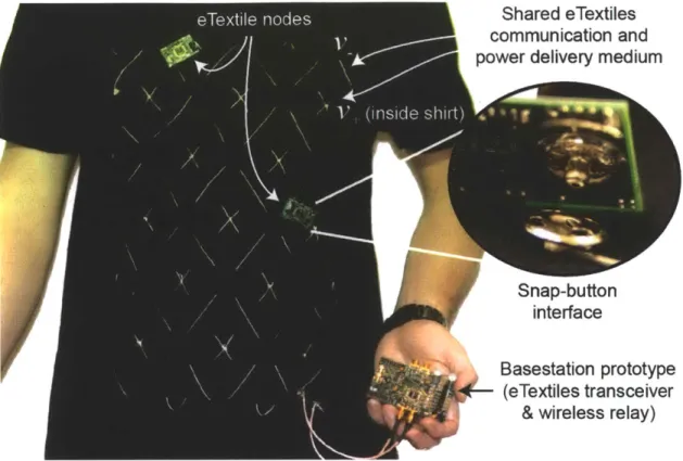
1-4 A body-area network for local communication of sensor data using both wired eTextiles and wireless RF circuits. . . . . 30
2-1 Various conductive fabrics for use as eTextiles communication mediums. 42 2-2 Implemented eTextiles-based body-area network system using
conduc-tive yarn as a time-shared communication and remote charging medium. 43
2-3 Packet diagram indicating when sensor nodes and the basestation
trans-mit, receive, and enter the remote charging phase. . . . . 44 2-4 eTextiles transceiver block diagram. . . . . 45
2-5 Supply-rail-coupled differential ternary transmitter front-end. . . . . . 48
2-6 Simulated supply-rail-coupled transmitter timing diagram for
trans-m itter T X +. . . . . 50 2-7 Block diagram of the eTextiles receiver. . . . . 52 2-8 Common-mode independent supply-rail-coupled sample-and-hold schematic
diagram . . . . 53 2-9 Sampling switch boosting circuit, enabled when operating at supply
voltages below 1V. . . . . 54 2-10 Simulated supply-rail-coupled sampling transient waveforms. . . . . . 55
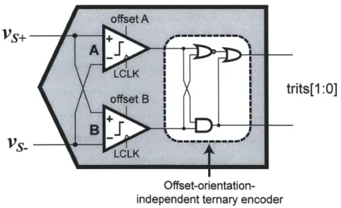
2-11 Block diagram of the 1.5-bit flash-like ternary ADC. . . . . 56
2-12 Programmable-offset comparator (pre-charge transistors not shown). . 57 2-13 Measured offset profile of two comparators in an AQ unit. . . . . 59
2-14 Offset error distribution of 72 different comparators, measured across
9 different chips. The comparator configuration redundancy improves
the standard deviation of offset errors by 2.1X in this case. . . . . 60 2-15 Receiver back-end used for synchronization between the transmitter
2-16 An illustrative beacon transmission and the corresponding interleaved
sampling clocks. Since each AQ unit samples for one half clock period every two cycles, two beacon codes are interleaved such that only a single AQ unit captures the appropriate data. . . . . 63
2-17 System medium access protocol with packet diagram repeated for
con-venience. . . . . 65
2-18 Die photograph of the eTextiles transceiver. . . . . 67 2-19 Measured transient response across the eTextiles network, illustrating
a typical packet request by the basestation. . . . . 68 2-20 Measured receiver bit error rate (BER) curves and combined receiver
and transmitter front-end energy consumption as a function of the effective differential voltage swing seen on the 1m eTextiles network. . 69 3-1 Various energy harvesting sources located external (black) or in-vivo
(red) to the body. Scalable solutions use power density estimates, while non-scalable solutions use total extractable power estimates. . . . . . 76
3-2 Diagram of the outer, middle, and inner ear. The ossicles (middle ear
bones) are highlighted in white text. . . . . 81
3-3 Illustrative diagram of the cross section of a single turn of the cochlea. 82
3-4 Detailed illustration of the operation of a single hair cell. Ionic cur-rents, consisting mostly of potassium ions, depolarize the hair cell, opening voltage-actuated calcium channels, which cause the release of neurotransmitters, which elicit action potential firings in afferent nerves. 84
3-5 Detailed illustration of the ionic flow occurring inside the cochlea. . . 87 3-6 Circuit model of circulating potassium current as generated by the
endocochlear potential. . . . . 88
3-7 Block diagram of the endoelectronics chip. . . . . 93 3-8 Leakage performance of a representative NMOS device plotted versus
the device width. Clearly, the lowest leakage current is found with a greater-than-minimum width. . . . . 95 3-9 The maximum frequency of NMOS and PMOS devices whose widths
are optimally sized, plotted for various lengths (in ym) versus normal-ized leakage power. . . . . 97 3-10 Schematic diagram of the boost converter power train and its simplified
control logic . . . . 98 3-11 Timing diagram of the boost converter power train illustrating overall
system power supply behavior . . . . 99
3-12 Schematic diagram of the charge-pump circuit. . . . . 100 3-13 Block diagram of a typical energy-efficient UWB transmitter. . . . . . 103
3-14 Simplified block diagram of the proposed direct-RF power oscillator transm itter. . . . . 104
3-15 Electromagnetic simulation setup in IE3D. The various rectangular
layers represent different substrates or tissues. . . . . 108 3-16 Electromagnetic simulation results for varying the antenna height for
3-17 Radiation pattern of the 3 x 4 mm2 loop antenna embedded in biolog-ical tissue. . . . . 112
3-18 Electromagnetic simulation results for wireless power transfer to the
implant for initial programming under a simultaneous conjugate match-ing condition. . . . . 113 3-19 Detailed circuit schematic of the 2.4 GHz radio transmitter with
inte-grated wireless energy receiver. High-Vt switches are shown in green, and signals operating from the charge pump supply are shown in red. 114
3-20 Simulated results of the resonant tuning capacitive DAC together with
the fixed inductive loop antenna. . . . 116
3-21 Simulated capacitor quality factor versus parasitic switch capacitance
for single-ended and differential switches. . . . . 117 3-22 Current-starved ring oscillator schematic. High- devices are shown
in green. ... ... 118 3-23 Circuit schematic of the 7-bit (5-bit output) counter, with the 5-bit
comparator used to set the transmitted packet length. . . . . 119
3-24 Schematic diagram illustrating the relationship between the endocochlear potential and the instantaneous output data rate. This relationship can be exploited to create a built-in wireless endocochlear potential sensor. 121
3-25 Measured relationship between the ring oscillator power supply and its
characteristic frequency. . . . 121
3-26 Microphotograph of the endoelectronics chip. The core area occupies
1.2 m m 2. . . . 124
3-27 Photograph of the endoelectronics testing and prototyping platform,
showing the daughter card containing the chip and the main board hosting the FPGA interface. . . . . 125 3-28 Photograph of the miniaturized endoelectronics chip-on-board on a
human index finger. Dam-and-fill epoxy encapsulation is not shown for clarity. . . . 126
3-29 Measured efficiency of the boost converter power train as the input
impedance of the boost converter is swept. . . . 127
3-30 Amount of output power available to any load circuit powered by the
boost converter, harvesting energy from a circuit model of the endo-cochlear potential. . . . 128
3-31 Active-mode output power of the radio transmitter measured from a
2.4 GHz A/4 whip antenna with 2 dBi gain placed approximately 5 mm from the on-board loop antenna, plotted versus power oscillator current configuration settings. Actual radiated power is expected to be higher than these results, though it is not possible to measure this directly. . 130
3-32 Measured active-mode power consumption of the transmitter plotted
3-33 Transmitter radiated efficiency, measured as the ratio of radiated
out-put power over total consumed power in the transmitter, plotted versus power oscillator current configuration settings. The actual transmitter efficiency is expected to be higher, due to the uncertainty in output power measurements. . . . . 131 3-34 Measured OOK spectra taken using a A/4 whip antenna a few
cen-timeters from the on-board loop antenna. . . . . 133
3-35 Measured FSK spectra taken using a A/4 whip antenna a few
centime-ters from the on-board loop antenna. Here, Af = 0.7 MHz. . . . . 134
3-36 Measured wirelessly-received transient waveform, illustrating a startup
tim e of 180 ns. . . . . 135 3-37 Measured wirelessly-received transient waveforms of the transmitter
with randomly-modulated 5 Mbps OOK data. . . . . 135 3-38 Measured frequency response of the capacitive DAC tuning range. . . 136 3-39 Measured phase noise of the power oscillator output. At 1 1MHz offset,
the phase noise is -105 dBc/Hz . . . . 137 3-40 Measured radiated output power plotted versus resonant frequency as
the capacitive DAC tuning bits are varied. . . . . 137 3-41 Ring oscillator frequency and power results, sorted in order of
increas-ing frequency. . . . . 139 3-42 Measured energy required for every cycle of the ring oscillator at VDD= 0.8 V.139
3-43 Measured standby power of the radio transmitter plotted versus various system supply voltages. . . . . 141 3-44 Average power of the radio transmitted plotted over an extremely wide
range of duty-cycled data rates, compared to other work. . . . . 142 3-45 Energy consumed per transmitted bit of the radio transmitted plotted
over an extremely wide range of duty-cycled data rates, compared to other work. . . . . 143 3-46 Photograph of electrode insertion through the round window of a guinea
pig in order to interface with the endocochlear potential. . . . . 146
3-47 Simplified illustration of the clinical experiment setup. The endoelec-tronics chip was initialized with a one-time wireless energy packet, after which the system extracted energy from the endocochlear poten-tial. High-impedance multimeters monitored VDD, VPUMP, and VEP
while an external radio demodulated wirelessly received packets. . . . 147 3-48 Clinical measurement result showing the first demonstration of an
elec-tronic system sustaining itself with the endocochlear potential acting as the only source of energy into the system. . . . . 148 3-49 Clinical measurement result showing three separate VDD traces for
three separate experiments. The average DC-value of each trace, along with its energy recovery slope is determined by the individual animal's endocochlear potential, the realized electrode impedances, and the con-figurable packet rate (the packet rate only affects the average DC level, not the energy recovery slope) . . . . 149
3-50 Transient measurement of a representative wirelessly received and
de-m odulated packet. . . . 150 3-51 Results showing that the instantaneously received data rate can be used
as an accurate proxy to measure relative changes in the endocochlear potential. . . . 151 4-1 An introductory schematic overview of a typical inductively-coupled
system . . . . 158
4-2 Schematic model of an inductively coupled system. In this case, series capacitors C1 and C2 are used to resonate with inductors L1 and L2. . 160
4-3 Resistive divider circuit. . . . . 162
4-4 Circuit model of a loosely-coupled transformer, and its load-reflected equivalent. . . . . 163
4-5 The four basic options for resonant tuning of inductively coupled coils. 163 4-6 Converting a parallel-tuned secondary to a series-tuned secondary. . . 164 4-7 Equivalent circuits for a series-turned secondary. . . . . 166
4-8 Load impedances that maximize power transfer. In this example, V, = 3.3 V,_,,
f
= 6.78 MHz, Li = 3.3 puH, L2 = 6.7 pH, Q1 = 60, and Q 2 = 80. . . . . 1704-9 Charging a capacitor at DC with a voltage step. . . . . 173
4-10 Transient results of charging a 1 F capacitor from a 1 Q source impedance to 1 V . . . . 174 4-11 Model used to calculate instantaneous charging capacitor resistance. . 174 4-12 Plot of RL,Opt over all practical values of k for three different values
of L2. In this example, V, = 3.3 V,_,,
f
= 6.78 MHz, Li = 3.3 pH,Q1
= 60, and Q2 = 80. The maximum output power is identical to thepower-optimized curve shown in Figure B-1(b). . . . . 177
4-13 Power delivered to RL across various values of RL and a few select values of k. In these plots, the blue, green, and red curves correspond to secondary inductances of 0.1 pH, 1 pH, and 10 pH, respectively. Additionally, V, = 3.3 V,_,,
f
= 6.78 MHz, L1 = 3.3 pH, Q1 = 60,and Q 2 = 80. . . . . 178 4-14 Architecture of the proposed multi-tap-secondary rapid wireless
capac-itor charger... 179
4-15 Electromagnetic simulation setup of the multi-tapped secondary and conventional primary coils. . . . . 182
4-16 Simulated coupling coefficients for various coil separation distances. . 183
4-17 Photograph of the secondary three-tap coil. . . . . 183
4-18 Power delivered to RL across various values of RL and a few select values of k. In these plots, the blue, green, and red curves correspond to secondary inductances of 0.28 [pH, 1.25 tH, and 6.73 pH, respectively. Additionally, V, = 3.3 Vpp,
f
= 6.78 MHz, Li = 3.3 pH. Q1,eff = 48,Q21,eff = 2.8, Q22,eff = 11, and Q23,eff = 42. . . . . 184 4-19 Photograph of the testing setup for the rapid wireless capacitor charger. 185
4-20 Power delivered to a Keithley 2400 sourcemeter set at fixed voltage values for a few select distances. In these plots, the overlaid solid blue, green, and red curves correspond to inductors L21, L22, and L2 3,
respec-tively. The light dashed green line corresponds to a fixed secondary tap configuration (i.e., without any series switches). Here, V, = 3.3 Vp-p and
f
= 6.78 M Hz. . . . . 1874-21 Measured power delivery compared to analytically predicted power de-livery under the same conditions as in Figures 4-18 and 4-20. . . . . . 188 4-22 Transient measurement of charging a 2.5 F ultra-capacitor to 5 V. The
thin blue, green, and red lines corresponds to exclusive use of inductors L2 1, L22, and L23, respectively, while the thick black line corresponds dynamic switching between them. . . . . 189
4-23 Charging time for a 2.5 F, 5 V ultra-capacitor. The thin blue, green, and red dashed lines corresponds to exclusive use of inductors L21, L22,
and L23, respectively, while the thick black line corresponds dynamic
switching between them. . . . . 190 4-24 Block diagram of a simple power monitoring circuit which can be used
to select which of the three taps offers the highest power transfer. . . 192
5-1 Diagram of a nanorobot harvesting energy from intracellular potentials. 200 B-1 Efficiency and load power delivery for a power-transfer-optimized link
and an efficiency-optimized link. In this example, V, = 3.3 V,_,,
f
= 6.78 MHz, L1 = 3.3 puH, L2 = 6.7 pH, Q1 = 60, and Q2 = 80. . . .. 207 C-1 Generalized circuit to modify the effective instantaneous capacitorre-sistance, Rc,eff to look like the optimal load rere-sistance, RL,opt, for maximum power transfer. . . . 209 C-2 Modulating Rc,eff using a DC/DC converter. . . . . 210
C-3 Using a matching network to convert resistances. . . . . 211
C-4 Using a resistance compression network to convert and normalize re-sistances . . . . 212
List of Tables
2.1 Comparison of Body-Area Network Communication Systems ... 70 3.1 Comparison of various energy harvesting sources. . . . . 79 3.2 Calculated and simulated 3 x 4 mm2 loop antenna in free space and
biological tissue environments at various ISM band frequencies. . . . 109
3.3 Simulated transmitter power breakdown across process corners and
voltage variation. . . . . 123
3.4 Measured quiescent power breakdown of various blocks in the boost converter. . . . 127
3.5 Measured active-mode power breakdown of various blocks in the radio transmitter operating at 0.8 V and at a frequency of 2.48 GHz. . . . . 132
3.6 Measured transmitter standby-mode power breakdown at various
sup-ply voltages compared to simulated results. . . . . 140
3.7 Comparison of previously published energy efficient and/or low power
narrowband transmitters . . . . 144 4.1 Comparison of energy storage elements. Estimated values come from
a 1 cm3 energy storage element. . . . . 157
Chapter 1
Introduction
Semiconductor process scaling has been fueling the growth of the computer and elec-tronics industries for decades. Since the invention of the integrated circuit (IC) by Jack Kilby and Robert Noyce in the late 1950s, process scaling has faithfully followed Moore's Law, which states that the number of transistors on a single chip will dou-ble every two years. To put this into perspective, Moore famously said "if the auto industry advanced as rapidly as the semiconductor industry, a Rolls Royce would get a half a million miles per gallon, and it would be cheaper to throw it away than to park it" [1].
Integrated circuits following Moore's Law have been transformational when it comes to the computer industry. A vacuum-tube-based computer that weighed more than 30 tons and consumed 20 kW of power in 1946 is easily surpassed in performance
by small, hand held devices today [2]. To put this in perspective, consider that the
General Purpose Computer (GPC) on board NASA's space shuttles in the 1970s had roughly the same computational throughput as a circa 1980s IBM 5150 processor with
500 kB of memory [3]1. An Xbox 360 has 20,000 times the processing horsepower. However, as all technologies mature, the theory of diffusion of innovations suggest they tend to become commoditized [4]. By creating new or disrupting existing
appli-cation spaces, the microelectronics industry has shown remarkable agility in finding
'Remarkably, NASA continued to use essentially the same computer until the Space Transporta-tion System program was shut down in 2011. This is a classic example of "don't fix it unless it's broken".
new growth opportunities. As shown in Figure 1-1, new areas of growth have consis-tently been exposed every decade over the past forty years. For example, after a very long period of exponential growth, margins in the personal computer (PC) market are at all-time lows, which is the direct result of desktop and laptop computers becoming commoditized. Advances in integrated radio-frequency (RF) circuits using cheaply available CMOS technologies propelled the communication markets in the 2000s, and together with miniaturized computers, have created the currently expanding portable consumer electronics market.
Watches Calculators Computers Communications Consumer Medical
1970
1980
1990
2000
2010
2020
Figure 1-1: Industries disrupted by microelectronics. Courtesy of MEDRC/Mara Karapetian.
Due to significant growth opportunities, personal medical electronics has been identified by many as the next market ripe for disruption by microelectronics. For example, a report by Parks Associates suggests that digital home-based healthcare is projected to grow from an already large $1.7 billion market in 2010 to a $5.7 billion market in 2015, with anticipated exponential growth following this [5]. Given such economic projections, there is much activity beginning to develop in this area.
However, with the exception of certain key applications, the personal medical electronics market has been largely untapped until very recently. Not surprisingly, biomedical electronic devices that have been on the market for a while have typically been used in applications where circuits are simple and there is sufficient volume to support the resulting system. For example, artificial cardiac pacemakers, first designed in the 1960s, are low-complexity oscillators that have the luxury to fit in a 60 mm diameter and 10mm thick disc. Even when consuming 10 [A, a 600 mAh battery (which could, even in the 1960s, fit in such a package) allowed for up to 5
years of operation before surgical replacement was necessary [6]. In 2002, there were 3 million people with implanted artificial cardiac pacemakers worldwide, with 600,000 additional devices being implanted per year [7]. Similarly, cochlear implants, which
help deaf patients re-create the sensation of sound through neural stimulation, have
been implanted in over 219,000 people worldwide as of December 2010 [8,9].
So if integrated electronics and Moore's law have enabled these particular appli-cations, in some cases decades ago, why is it only now that significant industry-wide activity is being seen in the biomedical electronics area? While there are undoubtedly many reasons, there are two significant interrelated societal factors that make now a good time for investment in research and development:
" Aging Population: The US baby-boomer generation consists of approximately
76 million people. In 2006, approximately 12% of the US population was over the age of 65. By 2030, when the last of the baby boomers are expected to retire, the number of Americans over the age of 65 will increase to roughly 20% of the population [10]. Consequently, the number of people needing frequent access to basic healthcare services is expected to increase significantly.
" Healthcare Costs: In 2010, the United States spent $2.6 trillion on
health-care, which is roughly 17.9% of the country's GDP. By 2020, healthcare costs
in the United States are expected to outpace economic growth and comprise 19.8% of GDP, or $4.6 trillion [11]. Similarly, total Medicare expenditures were $523 billion in 2010, which is roughly 3.6% of GDP. Left unchecked, Medicare expeditures are projected to grow to 10.7% of GDP in 2085 [12]. Regardless of the accuracy of these predictions, it is clear that any advances in biomedical electronics that offer the potential for reduced healthcare costs will be a boon not only to human health, but also to the economy.
Additionally, there are three significant technological factors that are beginning to enable this emerging biomedical electronics market:
* Semiconductor Scaling: Continued process scaling is not necessarily required
for the design of implanted or body-worn devices. In fact, many implants are designed in standard 0.18 prm Complimentary Metal Oxide Semiconduc-tor (CMOS) processes or older, mostly due to their excellent analog properties and low-leakage characteristics. Instead, continued semiconductor process scal-ing facilitates higher-performance external computational resources, which can be used to process biological data for monitoring applications and closed-loop actuation systems, or can be used for advanced modeling of biological processes. These computations are typically not performed on the implant or wearable de-vice itself, but are instead performed by a high performance processor located on a smart phone, PC, or a remote server farm in the cloud. Examples include machine learning algorithms to detect seizures in epilepsy patients [13], or neu-romorphic electronics deriving inspiration from neural networks for accelerated biological simulations or processing [14].
* Clinical Understanding: With improved computational resources and
biomed-ical electronic devices, clinicians are able to perform new experiments and ana-lyze larger and more complex data sets, creating an environment well suited to expand basic scientific knowledge of underlying biological processes. With ex-panded understanding, it is possible to better identify where and why sensing or actuation of biomedical electronic interfaces can be beneficial, and consequently, how biomedical electronic devices can be improved.
* Miniaturization: Unlike PCs, which can be as large as necessary (within
reasonable limits), personal medical electronic devices necessitate small form factors due to aesthetics and, more fundamentally, anatomy. Although process scaling has typically been the trump card for miniaturization of microelectron-ics, battery technology has not followed suit. Consequently, energy efficiency and/or energy autonomy together with advanced packaging technologies are the most promising method of reducing biomedical electronic device volume. This is of particular importance to implanted and body-worn devices, where, in
sharp contrast to PCs, total system volume (including all peripheral electronics and energy storage elements) must be on the order of anywhere from a few cubic centimeters to a few cubic millimeters. Energy efficient designs based on techniques and technologies developed at universities and industrial research and development centers are beginning to enable very interesting and benefi-cial biomedical electronic systems such as artifibenefi-cial pancreases [15] or epileptic seizure monitoring systems [16], that can approach the size of cubic
millime-ters [17].
The high-level goal of the research presented in this thesis is to explore the personal biomedical electronics design space, with an emphasis on increasing energy efficiency and autonomy metrics in order to create devices that are sufficiently miniaturized to fit within the anatomical constraints typical of biomedical applications. Pushing such energy metrics for wearable and implantable devices beyond the state-of-the-art requires innovation and optimization not only at the circuit level, but also, and perhaps more importantly, at the system level.
Regardless of the specific application, many personal wearable or implantable biomedical monitoring or actuation devices share four common requirements. The first and most obvious requirement is that such devices must interface in some manner with the underlying biological process. For example, an electrocardiography (ECG) monitoring patch must capture the inherent electrical activity of the heart, while an artificial cardiac pacemaker must electrically stimulate the heart if the natural electrical conduction system is damaged. The second requirement is that most such devices must communicate with the outside world. Communication is required in order to transmit sensed data, for example from an ECG monitoring patch, or to receive commands, for example to change the pacing frequency of an implanted pace-maker. Thirdly, such devices must process and manage their energy effectively. Bat-tery management circuits and efficient power converters are required to make the most of limited energy budgets. Finally, many, but not all biomedical electronic sys-tems also require some on-board signal processing. In some cases a trade-off exists where processing and compression of data can substantially reduce communication
requirements, thereby altering the system energy allocation budget [16]. A gener-alized biomedical electronic system featuring these requirements is shown in Figure 1-2.
Energy Harvesting Energy Storage
++
Figure 1-2: A generalized wearable or implantable biomedical electronics platform for personalized monitoring or actuation. On-board signal processing (shown in the dashed box) may be extremely beneficial in many cases but is not required for all applications.
Typically, communication circuits dominate the power budget of such nodes [18]. Consequently, efficiency improvements of communication sub-systems together with their corresponding energy management circuits can directly lead to increased minia-turization through the use of smaller energy storage or harvesting elements. As a result, the more specific goal of this thesis is to investigate communication and en-ergy delivery sub-systems in order to maximize enen-ergy efficiency. Both wearable and implantable application spaces will be explored.
1.1
System Design Philosophy
The research and design philosophy used throughout this thesis relies on a three-pronged approach to achieve anatomical miniaturization through energy efficiency and energy autonomy. This philosophy spans multiple layers of design, from low-level transistor optimization to high-level system considerations.
1. Use-case engineering: The most powerful way to achieve miniaturization or advance functionality is by considering the use-case of the system. Careful consideration as to how a patient may use a particular system can lead to new design approaches at the circuit, algorithmic, and architectural levels. In some cases, the use-case and resulting system implementation is straightforward, and no further design insight is gained. However, in other cases it may be possible to slightly change the use-case in a manner that does not negatively affect overall system experience, with dramatic implications in terms of system size or functionality. For example, Chapter 4 of this thesis discusses a change in the user experience that eliminates the requirement of a semi-permanent external wireless energy source used to power an implant. Instead, a fast once-a-day charging paradigm is proposed, permitting a fully implanted system that does not have the aesthetic or practical concerns of a relatively large semi-permanent external attachment.
2. Architectural optimizations: After system usability is carefully considered, the resulting system architecture should be optimized to fit the modified use-case. In some cases, a modified use-case lends itself directly to novel architectural requirements with implications in energy, size, or usability. In other cases, architectural transforms are inherently necessary to achieve energy efficiency, independent of the specific use-case. For example, the work presented in Chap-ter 2 discusses an electronic textiles system for communication of sensor data around the human body. Since communication is achieved over a two-wire in-terface, the transceiver architecture can be modified to further permit power
delivery over the very same network, enabling capacitively-buffered, energy au-tonomous sensor nodes of minimal size.
3. Circuit techniques: Classical circuit optimizations are also required to maximize
system integration and energy efficiency. Such optimizations include device se-lection, transistor sizing, layout considerations, wire engineering, passive design, and sub-block topological design. Chapter 3, for example, describes how very careful analysis of transistor leakage characteristics, together with an extremely duty-cycled energy buffering architecture, can enable the design of an ultra-low-power radio transmitter that can operate on sub-nanowatt ultra-low-power budgets.
In many cases, two additional steps can be employed to further system efficiency or functionality. Applications of advanced algorithms for both communication [19] and data analysis/compression [16], as well as device engineering can substantially increase overall system energy efficiency. These topics will not, however, be discussed in detail in this thesis.
1.2
Wearable Bio-Monitoring Devices
One current thrust in the area of personal medical devices is to transition medical monitoring operations away from expensive hospital environments and move them towards the home. So-called telemedicine or connected health systems employ the use of body-worn sensor nodes for remote monitoring of vital signs or other physiological signals [20-23], as illustrated in Figure 1-3. Monitoring of this nature is not only useful for patients with chronic conditions, but can also be valuable to those at high risk of medical emergencies (e.g. a monitoring system could alert an ambulance at the onset of a heart attack), or those undergoing physical stress (e.g. monitoring
dehydration in athletes or soldiers).
From a patient's perspective, a key metric for such wearable devices is operational lifetime; that is, the length of time the device can operate before its energy storage element (e.g. a battery) must be completely re-charged. As previously discussed,
.
Physiologic Data
World Wide Web
Patient Physician Medical Monitoring FacilityFigure 1-3: A typical medical monitoring system, where a patient's physiologic signals are transmitted to the Internet for examination by a physician or a remote monitoring server.
communication circuits often dominate the power budget of sensor nodes, thereby limiting the achievable operational lifetime per unit battery weight. This is partic-ularly evident when using wireless circuits for communication distances in excess of
10 m, where power amplifier (PA) power consumption scales directly with transmit
distance and ends up dominating the entire system power budget [24].
From a system perspective, it makes sense to push complexity away from locations where weight and volume (and as a result, energy) are constrained, and move this complexity to locations where energy is more abundant. Thus, rather than having each sensor node communicate directly over a cellular or WiFi-type of network, it is beneficial to have body-worn sensor nodes communicate over a local body-area network (BAN), as illustrated in Figure 1-4. This limits communication distances to under a few meters, pushing the bulk of the transmit power requirements to an energy-rich local relay (e.g. a cellular phone or pager-type device). This also permits
BAN users to self-monitor, provided the local relay has a display or other notification
mechanism.
Unfortunately, even when communication distances are on the order of one meter, communication circuit power still often dominates the power budget of sensor nodes. Due to short transmit distances (and therefore limited required radiated power), the
power budget is not completely dominated by the transmitter's PA in this situation; instead, the receiver front-end constitutes a large fraction of system power [25].
eTextiles Grid Surface Sensor - -Personal Basestation Wireless 1m link eTextile RX 10-100m link TransmitterZ *
Figure 1-4: A body-area network for local communication of sensor data using both wired eTextiles and wireless RF circuits.
As a result, it is still imperative to increase the energy efficiency of communication circuits in order to achieve the desired goal of small, long-lasting body-worn sensor nodes, even in the limit of short transmit distances. The proposed work addresses this requirement by exploring the use of eTextiles as a communication medium for body-area networks, also shown in Figure 1-4. Since nodes are effectively coupled together via a wired link, extreme efficiency is possible for both data communication and energy delivery, ultimately permitting smaller nodes that have longer operational lifetimes. A system-on-chip (SoC) was built to communicate and deliver energy over a network-on-shirt, and is described in Chapter 2.
1.3
Implantable Bio-Monitoring Devices
Patients with implanted devices are most certainly concerned with operational life-times.2 However, often times a metric of greater importance is implanted device lifetime. In this case, implanted device lifetime refers specifically to how long the de-vice can function before surgery is required to replace the implant, typically because a battery has been depleted of energy or has exceeded the recommended number of re-charging cycles.
Fortunately, reducing the energy consumption of implanted circuits addresses both operational and device lifetime concerns. However, it is not always possible to
sim-ply reduce energy consumption. Electrical stimulation of nerve fibers, for example,
requires a fixed amount of power that appears to be fundamentally limited by neu-ral strength-duration curves [26]. Similarly, sensing of physiologic signals such as electroencephalography (EEG) or ECG waveforms require instrumentation amplifiers that consume current that is fundamentally limited by noise constraints [27,28]. Since it is not possible to reduce energy consumption below certain fundamental limits, the only way to increase operational and device lifetime is by either increasing the size of the energy storage element, or by extracting and harvesting energy from locally available sources.
Many of today's implanted devices such as retinal implants and deep brain stim-ulators rely on continuous wireless power transfer from an external source [29, 30]. Constant wireless power delivery is particularly relevant when the implant does not permit the installation of a battery, either through anatomical volume constraints, or because it is not practical to perform additional surgeries3 when the battery even-tually fails. In this case, the implanted device lifetime is essentially infinite - the implant potentially never needs to be surgically replaced. However, the implant
oper-ational lifetime is essentially zero -an external energy source must always be present. Furthermore, the external energy source must be much larger than an equivalent im-planted energy source by at least a factor of 1/, where q is the wireless power transfer
2As a reminder, operational lifetime is the span of time a device lasts between re-charge cycles. 3For example, due to a build-up of scar tissue or additional risk of infection.
efficiency, for equivalent system operational lifetime. Since 7's are generally very poor for these types of schemes (often much less than 50%), external energy sources, which must be worn at all times, can become uncomfortably large for patients. Addition-ally, such semi-permanent external sources often have poor aesthetics, and prevent patients from undertaking certain activities4 without losing access to the implant's
functionality.
To address the latter problems, one solution is to install an implanted battery and rely on a once-per-day charging use-case. This allows the patient to use or access the implant's functionality without requiring a semi-permanent externally-worn power
source. However, there are two significant issues with such an approach. First, as previously alluded to, a battery has a limited number of recharge cycles before its internal electrochemical cells wear out. Consequently, implanted device lifetime is limited, and surgical re-implantation will eventually be required to replace the battery. Second, batteries require a relatively long time to charge. For example, standard lithium-ion batteries typically require at least an hour to fully charge, regardless of the battery size [31, 32]. This charging time can be a major inconvenience for patients. Since approximately 50% of patients do not even follow their medication plans properly [33], it is imperative to make implantable devices as easy to use as possible. A shorter charging time would alleviate this particular inconvenience.
This thesis proposes two separate energy delivery and communication schemes to ease operational use of implanted devices. Significant changes over conventional implants at the use-case and architectural levels are proposed in order to increase both implant and system operational lifetimes, while keeping an essentially unlimited
device lifetime. The first scheme relies on energy harvesting techniques to
continu-ously power an implant without the requirement of a battery. Specifically, energy is extracted from an in-vivo electrochemical potential that exists naturally within the inner-ear of mammals. A fully-functional system prototype is presented in Chapter 3, which includes a description of the energy management and load circuitry. Since the available power from this energy source is extremely small, its use is limited to sensing
4
and communication applications of slowly-varying biological signals. As discussed in Sections 3.6 and 5.2, these applications can be extremely important and perhaps even transformational for patient diagnostics, monitoring, or basic scientific research.
For applications requiring higher power or energy density than is available from
the source described in Chapter 3, a second power management scheme is proposed
that relies on once-per-day charging of an implanted ultra-capacitor. The benefit of using an ultra-capacitor as an energy storage element is that charging times can be orders of magnitude faster than batteries - minutes rather than hours, for example.
So although the energy density of ultra-capacitors may be smaller than comparable-sized batteries, rapid charging enables the once-per-day charging use-case without significantly affecting patient usability. Additionally, since ultra-capacitors can be re-charged upwards of 1,000,000 times without a significant degradation in perfor-mance [34], system device lifetimes can last the duration of a patient's lifetime, never requiring surgical re-implantation. Chapter 4 presents a prototype wireless charger geared toward such a fully-implanted system.
1.4
Thesis Contributions
Broadly, this thesis examines the design of communication and energy management technologies for personalized biomedical devices. The ultimate goal of this work is to design systems that are suitably miniaturized to fit within the anatomical constraints of typical biomedical applications. This is primarily accomplished by increasing en-ergy efficiency, in some cases in combination with enen-ergy harvesting, in order to eliminate the requirement of large energy storage devices. The main contributions of this thesis are in the following four areas:
1. Electronic textiles system-on-chip - An eTextiles transceiver that
communi-cates over electronic textiles as an alternative, energy-efficient communication
medium for BAN applications is presented in Chapter 2. The proposed eTextiles
network architecture consists of a two-wire conductive yarn medium, body-worn nodes, and a basestation used for data collection and medium-access control.
The eTextiles transceiver employs supply-rail-coupled differential signaling to efficiently time-share the eTextiles medium between communication and remote charging activities. Remote charging achieves up to 96% power transfer effi-ciency over ohmic network and switch losses when a basestation battery is used to charge remote capacitors, which are used as the power supplies of body-worn nodes. Fabricated in 0.18 pum CMOS and operating at 0.9 V, the receiver and transmitter front-ends together consume 3.2 pJ/bit over 1 m at 10 Mbps, which is at least 20X more efficient than conventional BAN (i.e., wireless) re-ceiver front-ends. The transre-ceiver also contains an integrated digital baseband and medium access controller, which, together with the receiver front-end, con-sumes 110 pW during continuous operation.
2. Ultra-low power wireless implanted radio design - Due to anatomical volume limitations, implanted electronics are severely power constrained. However, not all implantable applications require frequent measurements or actuations. Such applications present an opportunity to design electronics that can be deeply duty-cycled, spending most of their time in ultra-low-power sleep states. Chap-ter 3 presents the design of a minimal-complexity 2.4 GHz radio transmitChap-ter that is designed specifically with aggressive duty-cycling in mind. Fabricated in a 0.18 pm CMOS process, the transmitter achieves a standby-mode power con-sumption of 39.7 pW, which is the lowest reported to date. In active mode, the transmitter requires 38 pJ to transmit a bit of information at an instantaneous data rate of 5 Mbps. When operating at a duty-cycle of 0.0001% by wirelessly relaying 128-bit packets every minute up to a distance of 1 m, the transmitter requires only 83 pW, which is over 10OX lower than previously published work.
3. System demonstration of energy extraction from the inner ear - The endo-cochlear potential is an electrochemical gradient naturally found within the inner ear of mammals. Due to limited extractable power, it has never before been used as an energy source for electronics. Chapter 3 of this thesis presents clinical measurement results of the first system demonstrated to sustain itself
with a mammalian-generated electrochemical potential operating as the only source of energy into the system. This was enabled in part through the afore-mentioned energy efficiency transmitter, which was integrated together with a boost converter, antenna, and three passives into a 9 mm by 11 mm chip-on-board package. Clinical results were obtained using the endocochlear potential of a guinea pig as the system power source over an experiment duration of five hours.
4. Rapid wireless ultra-capacitor charger - There are many additional implant ap-plications that have larger power requirements than what is harvestable in-vivo in mammals. As a result, implantable energy storage elements are required. Since batteries take too long to charge, Chapter 4 proposes a once-per-day charg-ing use-case that employs an ultra-capacitor as the implanted energy storage element. Unlike conventional chronic wireless power delivery systems which en-deavor to maximize efficiency, the goal of this work is to minimize charging time for patient ease-of-use. This new problem formulation requires a re-investigation of standard inductive coupling theory in order to identify opportunities to im-prove charging time. Based on this investigation, Chapter 4 presents the design of a rapid wireless capacitor charger that uses a multi-tap secondary coil that dynamically alters the characteristic inductive coupling equations in order to deliver the maximum amount of transient energy to the ultra capacitor. The proposed technique enables charging times that are up to 3.7X faster than con-ventional approaches. Alternatively, the usable transcutaneous coil separation range can be increased by 2.5X. Although developed primarily for rapid charg-ing, the results presented in this thesis can also be applied to maximize power transfer efficiency.
Chapter 2
Electronic Textiles for Body-Area
Networks
Recent advances in sensor technologies are fueling new possibilities in personal health monitoring, where data is sensed and communicated away from the body for remote telehealth applications, as introduced in Section 1.2. For patient usability, sensing nodes must be small and light, thereby limiting the size of energy storage elements and requiring circuit and system solutions that are extremely energy efficient. Rather than directly interacting with a long-range wireless network, it is beneficial from an energy perspective for individual sensor nodes to communicate over a local body-area network (BAN), as illustrated in Figure 1-4. A dedicated local relay, such as a smart phone, can then collect sensor data to be transmitted over a long-range network to the Internet for monitoring purposes.
This chapter describes a system solution for not only communicating information around the human body, but also for delivering power to sensor nodes, obviating the need for a large battery. Both communication and power delivery is performed extremely efficiently through the use of a transceiver system-on-chip employing a wired electronic textiles (eTextiles) clothing network.
2.1
One-Meter BAN Communication
This section describes various means of achieving 1m body-area network communi-cation, and examines the strengths and weaknesses of each approach.
2.1.1 Wireless Communication
From a user's perspective, the untethered mobility gained by wireless communica-tions can, in certain cases, significantly improve freedom of patient movement. Un-fortunately, wireless communication suffers from several drawbacks which ultimately require high energy consumption, necessitating large form factor devices that as a
result can restrict freedom of movement.
Broadcasting
The broadcasting nature of wireless communication is simultaneously a strength and weakness when referring to BAN applications. On the one hand, omni-directional radiation of information encoded within electromagnetic (EM) waves is extremely convenient for the design of a single network in isolation. For instance, a transmitter and receiver do not need any a priori knowledge of their respective locations for successful communication, so long as they are within a pre-described distance of each other. Additionally, RF nodes are free to change their relative positions over time with little increase in processing overhead, so long as the rate of change of movement is slower than the duration of a single packet (which is generally true for human body movement).
On the other hand, broadcasting sensitive information over a wireless network raises significant privacy, security, and reliability concerns. To overcome these issues, the BAN must be designed to be robust to eavesdroppers (privacy), malicious at-tackers (security), and interference from other users (reliability).' As an example to combat privacy concerns, an advanced encryption standard (AES) engine could be
'Many other possible scenarios potentially affecting a wireless network exist and should be con-sidered [35].