HAL Id: hal-02319468
https://hal.laas.fr/hal-02319468
Submitted on 18 Oct 2019
HAL is a multi-disciplinary open access
archive for the deposit and dissemination of
sci-entific research documents, whether they are
pub-lished or not. The documents may come from
teaching and research institutions in France or
abroad, or from public or private research centers.
L’archive ouverte pluridisciplinaire HAL, est
destinée au dépôt et à la diffusion de documents
scientifiques de niveau recherche, publiés ou non,
émanant des établissements d’enseignement et de
recherche français ou étrangers, des laboratoires
publics ou privés.
Using infrared thermal responses for PCBA production
tests: Feasibility study
Nabil El Belghiti Alaoui, Anais Cassou, Patrick Tounsi, Alexandre Boyer,
Arnaud Viard
To cite this version:
Nabil El Belghiti Alaoui, Anais Cassou, Patrick Tounsi, Alexandre Boyer, Arnaud Viard. Using
infrared thermal responses for PCBA production tests: Feasibility study. 30 th European Symposium
on Reliability of Electron Devices, Failure Physics and Analysis (ESREF 2019), Sep 2019, Toulouse,
France. �hal-02319468�
__________________________________________ * Corresponding author. [email protected]
Using infrared thermal responses for PCBA production tests:
Feasibility study
Nabil El Belghiti Alaoui
a,b,*, Anaïs Cassou
a, Patrick Tounsi
a, Alexandre Boyer
a,
Arnaud Viard
ba
Laboratoire CNRS, LAAS, 7 avenue du colonel Roche, Univ. de Toulouse, INSA, LAAS, F-31400
b ACTIA Automotive, 5 Rue Jorge Semprun, 31400, France
Abstract
A Printed Circuit Board assembly (PCBA) testing approach using infrared thermal signatures is presented. The concept of thermal signature for PCBAs is introduced and proved by experience and simulation. Based on this concept, the testing method is able to detect assembly defects such as presence of the component, polarity, value and solder (shorts and opens) and in some cases component health state, it also can classify the components mounted on the PCB into two classes (fault-free, faulty). According to the thermal signature of each component on the PCBA, they can be also classified in the same classes. In this article focus is put on capacitor defects in a DC/DC converter, especially capacitor value defects. Therefore, they will be the main tested components. For a robust detection of multiple defect scenarios, the Principal Component Analysis (PCA) method is used as an outlier detection algorithm.
Keywords— Testability, Accessibility, defect detection, PCBA testing, thermal signatures, contactless testing, Principal Component Analysis, thermal modeling
1. Introduction
Traditional testing of printed circuit board assemblies (PCBAs) includes in-circuit test (ICT), visual inspection, x-ray radiography and functional test. These procedures are used to ensure quality, detect and eliminate defects, and accelerate weak component failures [1], [2]. Thermal imaging is one of the types of visual inspection that indicates hot spots on operating PCBs. These hot spots indicate shorts and overstressed components [1]. Traditional inspection equipment (visible-light or x-ray) are also useful on production lines, but such systems provide only physical “tests.” They can identify a fracture, a misplaced component, or missing solder, but problems such as a specific electrical short, a bad transistor, or a circuit that runs hot will all remain invisible [2]. Thermal imaging is very useful in the design and test process of PCBAs. Thermal signature analysis relies on the power dissipation of each component mounted on the PCBA. The energy dissipation associated with the current flow through the junctions in a semiconductor device or in a passive component gives rise to thermal characteristic of each component with respect to a certain test condition [1]. An infrared camera
captures this thermal characteristic of electronic components and thus the thermal signature is achieved according to the local emissivity. Further, the thermal image which is the association of different components thermal signatures can be used in the testing process of PCBAs. The deviation from reference thermal dissipation pattern or reference contour is a sign of fault occurrence. The color of each pixel in an infrared image, with the emissivity correction, represents a certain temperature in the real environment [3]. Infrared thermal defect detection achieves its results using only the information provided by the temperature evolution over time of each tested component. In order to test this defect detection approach, we used the temperature evolution of capacitors mounted on a DC/DC boost converter board [4] as heat signatures. The usual way of using infrared testing is to compare an acquired IR signature with a statistical model computed from IR signatures obtained from a set of known-good boards [5], [6]. The problem of this solution is to choose a proper threshold value and to compute and maintain the reference signatures from multiple PCBA samples.
The main goal of this article is to introduce the approach of using thermal signatures of components
ici
F1
F2
F3
FT InSb Infrared Camera
Powered PCB IC
Fig. 1. One-dimensional measurement of the IR thermal signature of a group of capacitors; with Φ1, Φ2, Φ3, ΦT being
respectively: the heat flux of components, heat flux of adjacents components, surrounding thermal noise, the total
heat flux measured by the camera.
mounted on a PCB in order to test them in production process. In-line testing based on components signatures is not a new concept; for example, using near-field magnetic signatures is described in [7] and [8]. On the other way, thermal signatures are usually used to conduct reliability tests and failure analysis of PCBAs and uncommonly used in the production process due to test-time constraints.
The organization of this paper is as follows. The concept of thermal signature of a PCB is introduced in the next section. The converter module and the experimental test bench are described in section 2.
Section 3 describes the achieved experimental results for simple defect cases and their analysis using the mean squared error (MSE).
In order to test multiple defect scenarios, we combined electrical circuit simulations that have been carried out on Cadence Orcad with a multi-physics model of the board under test (BUT) developed on COMSOL. Thermal simulation results are reported in section 5 to prove that component value defects can lead to measurable variations of the infrared heat signature.
For more robust defect detection on component level and thereafter PCBA level, an outlier detection algorithm based on Principal Component Analysis (PCA) is proposed and detailed in 5.3.1. Results are reported in 5.3.3. Finally, discussion and perspectives about the detection method are provided in conclusion.
2. The concept of infrared thermal signatures In this section, we introduce the concept of using infrared thermal signatures of components mounted on a PCB in order to identify assembly defects related to component value.
Components that will be focused on in this article are input and output filtering capacitors of a DC/DC converter. In power applications, these components are crucial to ensure a proper functioning and a good reliability of power management/power supply blocks. Moreover, they are usually hard to test in ICT especially when assembled in parallel groups of two or more different values. Testing them using their heat signature contactlessly will increase the testability of boards and optimize the quality of products.
2.1. Principle
Infrared thermal signature also called heat signature is the power dissipated by an electronic device or component by Joule effect in response to an electrical stimulus. This dissipated power is
radiated three-dimensionally as an infrared wave whose vertical component, in our case, is captured by a highly sensitive InSb IR camera [9] (see Fig. 1). In this first proof of concept, the stimulus used to trigger these signatures is a typical loaded operation of the BUT.
Detecting defective signatures will be achieved by comparing measured signatures to registered reference signatures. MSE indicator is a simple yet effective tool to compare signatures in the chosen defect cases, which are simple and will be detailed in the next section.
2.2. Case study & Test bench description
The set up used to prove the concept of this testing technique is shown in Fig.2. A highly sensitive mid-wave infrared (MWIR) camera which is equipped with cooled indium antimonide detectors with a resolution of less than 25mK. The camera produces temperature measurements with an accuracy of ±1°C and gives a wide temperature range that is automatically adjusted to best fit the thermal scene. A close-up lens (MW50MM) [10] is attached to the camera to achieve the necessary field-of-view. The frame rate was set-up at 25Hz and the integration time at 2ms because of the low operating frequency of the BUT and the low heating speed of the tested components.
The technique was tested on two different DC/DC converter boards with different topologies: a DC/DC buck converter and a DC/DC boost converter. The detection results were significant and
very similar on both cases. Therefore, only results from the DC/DC boost converter board (see Fig. 4) are presented. This board steps up a 3,6V input to a 9V output voltage at 170 kHz switching frequency [11].
The camera measures the temperature evolution over input and output capacitors under normal operating and loading conditions, which are summarized in Table 1. These measurements, which characterize each capacitor mounted on the board, will be referred to as infrared thermal signatures (IRTS).
Table 1
Operating and loading conditions
Input voltage / Output voltage 3.6V / 9V Input current / Output Current 2.5A / 0.9A
Resistive load 10Ω
Room temperature 23 °C
2.3. Test procedure
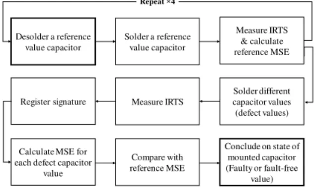
The test procedure used to prove the concept of the IRTS testing technique is shown in Fig. 3.
First, to prove the repeatability of measurements and that the IRTS’ variations are not due to the amount of solder used, reference value capacitors (22 µF) were desoldered and soldered repetitively while measuring IRTS’ of the mounted capacitor before each operation. The MSE was calculated for four repetitions of this first procedure (see Fig. 6).
Second, reference capacitors were desoldered and replaced by capacitors with the same dielectric technology and various defect values (4.7µF, 15µF, 33µF) separately and IRTS were measured for all input/output capacitors at each defect value. Capacitors were changed independently at each
measurement campaign for each defect value. Results for three defect values for each C1 and C4 are presented in section 3.
Third, MSE was calculated for every capacitor in comparison with the reference IRTS’. Conclusions about the capacitor’s value mounted on the PCB (Fault-free / Faulty) were made based on this comparison.
3. Results and analysis
The results presented in this section show that varying an input/output filtering capacitor value (C) has a direct influence on its temperature evolution (Tc) over time. The dissipated power depends on the equivalent series resistance (ESR) and the RMS current (icRMS) flowing through the capacitor (see equation 1). The RMS current, and thus the component temperature depends on capacitor’s value (see equations 2 and 3). A variation of the dissipated power captured by the IR camera serves as an indicator of value or solder (short / open) related defects.
Care was taken to choose ceramic capacitors that
Fig. 2. Figure showing the test bench, 1: the IR camera, 2: BUT, 3: computer station controlling the camera and the data
acquisition, 4: 10Ω load. Desolder a reference value capacitor Solder a reference value capacitor Measure IRTS & calculate reference MSE Repeat ×4
Register signature Measure IRTS
Solder different capacitor values
(defect values)
Calculate MSE for each defect capacitor
value Compare with reference MSE Conclude on state of mounted capacitor (Faulty or fault-free value)
Fig. 3. Test procedure used to prove the concept of the IRTS testing technique.
Input capacitors Output capacitors
Fig. 4. Simplified diagram of the BUT: DC/DC boost converter showing the tested capacitors.
(1) (2) (3)
have the same dielectric technology (see Table 2) in order to limit deviations due to value tolerance and temperature coefficient drift.
Table 2
Ceramic capacitors characteristics
C1 & C4
values (µF) Technology Package Tolerance
4.7 X7R 1210 10%
15 X7R 1210 10%
22
(Reference) X7R 1210 10%
33 X7R 1210 10%
3.1. Experimental results and analysis
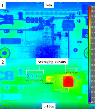
The software controlling the camera “ResearchIR” provides different pixel averaging cursors to measure the temperature evolution on the IR thermal image (see Fig. 5). A 3×3 pixels averaging cursor was put on each tested capacitor and the results of the first verification of the test procedure as mentioned in the first paragraph of part C are shown in Fig. 6.
These variations (see Fig. 6) are mainly due to the uncertainties related to the position of the soldered capacitors and to small value variation due to capacitor tolerance. Calculating the average MSE of the IRTS variation over each tested capacitor gives an average MSE threshold (MSETH) of 0.05 for each tested capacitor. This value will serve as a comparison value to detect signature variations when mounting a wrong value capacitor.
3.1.1. Reference Infrared Thermal Signatures
The averaging of the four IRTS measurements over each capacitor is presented in Fig.7 and used as fault-free reference IRTS’. For test in production, time constraints must be considered, which can vary from a manufacturer to another. An IRTS measurement over forty seconds was judged sufficient and can be optimized in function of the type of the BUT and the tested components.
3.1.2. Value defect in output capacitor C4
As discussed in the second paragraph of section 2.3, three faulty capacitor values were tested for C1 and C4. The results reflecting the IRTS variation over C4 are presented in Fig.8. A comparison between the calculated MSE for each component in this defect case is presented as a bar plot in Fig.9.
1 2 Averaging cursors Controller C1 C2 C3 C4 L C6 C7 t=100s t=0s
Fig. 5. IRT image of the BUT, 1: cold state, no power; 2: operating state, 100s of operation.
Zoom
Fig. 6. IRTS variation (doted lines) of all capacitors when desoldering and soldering C1 four times with the same
reference value. C1=C2=C3=C4=C6=C7=22µF 24,5 26,5 28,5 30,5 0 10 20 30 40 T em p er at u re ( C ) Time (s) C1 C2 C3 C4 C6 C7
Fig. 7. Reference IRTS’ of each input/output capacitor. C1=C2=C3=C4=C6=C7=22µF
Fig. 8. IRTS measured over C4 for three defect values in comparison with the reference IRTS.
Comparing the MSE calculated for each component shows that the highest MSE value (MSE_C4) corresponds to the defected capacitor C4 for all the three defected values. The MSE_C4 value was divided by 10 in order to fit into the comparison scale.
3.1.3. Analysis
In section 3, a simple statistical indicator was used to prove the concept of our test approach. It showed that the dispersion of wrong capacitor IRTS’ around the reference signature in a simple defect scenario (e.g. in which we introduced only one wrong value component) is higher in comparison with other capacitors with unchanged values.
In contrast with the PCB assembly industry, we must prove our solution in a scenario that takes into account multiple defects in the same capacitor set.
To do so, a multi-physics model of the BUT allowing the simulation of multiple defect scenarios in a much shorter time than experimentation is presented in the next section.
To use multi-physics simulation we must know all thermal characteristics of the BUT (materials and geometry), which is not always possible. To overcome this, the unknown parameters have been estimated to calibrate the model in order to have a thermal behavior similar to that of our case study.
4. Simulation results and analysis
4.1. Simulation set-up
We simulated the BUT on Allegro Design Entry [12] using the PSPICE model of the controller given by the manufacturer. Parasitic elements of capacitors were extracted using their references on SimSurfing [13]. Then, we ran multiple parametric simulations with different values for each output
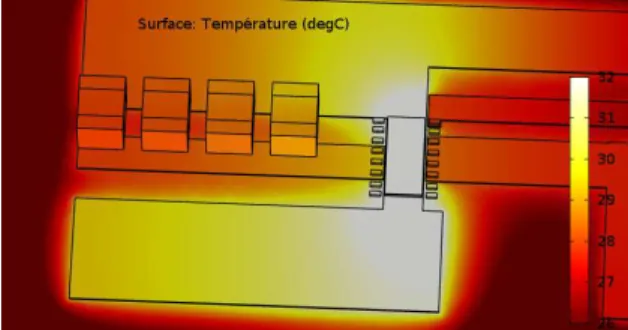
capacitor (see Table 3). The output of the electrical circuit simulation, which is the dissipated power of each capacitor, is then given as an input into COMSOL Multi-physics model of the BUT (see fig. 10).
This thermal simulation aims to give the thermal response of each output capacitor according to the power dissipation calculated from voltage and current waveforms.
4.2. Model description
A 3D thermal modelling of the BUT is performed using COMSOL Multi-physics in order to compute the temperature evolution of each component under test.
The components modeled are the capacitors, the controller and the inductor. Each capacitor is modeled with a ceramic block enclosed by Nickel metallization. Copper traces connecting the components are also represented. The PCB is represented as an FR4 layer (see Fig. 10).
Fig. 10. 3D thermal model of the BUT: operating state
Power dissipation is applied on each capacitor volume. Considering only heat transfer by conduction on the circuit board, pads are the only heat source for the inductor and the controller.. The inductor dissipates a power Pself = 37 mW calculated for an input current Iin = 2.533 A. The exact dissipated power of the controller is unknown as an input data. A first estimation is made using the operating current value and the maximum dissipated power from the component datasheet. The estimated power dissipation of the device is Pc = 200 mW.
The applied conditions at the boundaries are:
-
Convection with the ambient air at 23°C on the topwith htop= 30 W·m
-2
·K-1 and bottom with hbot =5 W·m-2·K-1 of the BUT. Heat transfer coefficients are calibrated in accordance with the experimental set-up and reference measurements of the temperature time evolution of the components.
- Adiabatic sides of the circuit board.
This simplified 3D model simulates with a satisfactory accuracy the thermal behavior of the BUT. However, approximations were made
0 0,02 0,04 0,06 0,08 0,1 0,12 0,14 0,16 0,18 C4=4,7µF C4=15µ F C4=33µ F M S E
Defect value introduced
MSE_C1 MSE_C2 MSE_C3 MSE_C4 ÷ 10 MSE_C6 MSE_C7
Fig. 9. MSE calculated for each input/output filtering capacitor for three defected values of capacitor C4
concerning the structure of the capacitors and the unknown data such as the dissipated power of the controller, which led to differences with measured temperature evolution.
4.3. Simulation results analysis: 4.3.1 Defect detection algorithm
IRTS’ of each capacitor are partially correlated. These correlations follow complex laws difficult to predict, which makes a defect indicator based solely on MSE insufficient to account for these correlations. Furthermore, in a PCBA production environment, a large number of variables will be generated, some of which might be correlated. A defect indicator based solely on MSE is insufficient to account for these correlations.
Principal Component Analysis (PCA) is one of the algorithms that can be used to transform the original variables to linear combinations of these variables called principal components (PC), which are uncorrelated. In this new coordinate system, the covariance matrix is diagonal and the first PC points into the direction with the largest variance within the data set. The PCs are the eigenvectors of the covariance matrix and its eigenvalues are the variance obtained with these new variables. Given the percentage of variation that we want to be captured in the abridged data set, we can select the number of PCs to be considered without a significant loss of information [14].
PCA is not only a technique to reduce the number of variables but can further be used for classification purposes based on the Principal Component Scores. Using PCA in our case will allow us to classify data into two categories: faulty PCBs and good PCBs, which will be presented next in an application on simulation data extracted from our DC/DC boost converter model. The simulation output is a data matrix of temperature evolution of four output capacitors. Thus, PCA calculates four Principal Components and arranges them in a descending order of variance [15].
In the following results, we choose the three highest variance PCs in order to plot the scores in a 3D graph for a clarity purpose.
4.3.2. Defect detection scenarios
Using the simulation model of our DC/DC boost converter, six non-faulty PCBs are generated with differences in terms of components values. They vary randomly according to their tolerance range using a uniform Monte-Carlo simulation. Among them, a faulty PCB with one or multiple value defects (see Table 3) in the output filtering capacitors block is inserted. The chosen capacitor’s wrong values are higher or lower than the reference value
and are outside of the tolerance range (22µF ± 10%). The input of the PCA algorithm is a 6-by-4 matrix composed of simulated IRTS measurements of four capacitors over six different PCBs.
Table 3
Simulated defect scenarios
N° Defect scenarios Details 1 One wrong value capacitor
a. The wrong value is lower than reference b. The wrong value is higher than reference
2 Two
wrong value capacitors
c. first wrong value is higher than reference;
second is lower than reference
d. Both wrong values are higher than reference e. Both wrong values are lower than reference
4.3.3. Defect detection results
A graphical presentation of the PC scores shows clearly which PCBs are faulty and considered as outliers (see Fig.11).
The first Principal Component (PC1) captures the most variation of the data- 92.67%- which is the ratio between the eigenvalue associated to PC1 and the sum of all eigenvalues. This ratio describes the contribution of a particular PC to the dispersion of the data.
In our case, the significant variation that can be used to detect capacitor value defects is related to PC2. Despite of the low data variation rate captured by this PC, PCBAs containing defected capacitors are still distinguishable when comparing the absolute value of their projected coordinates over PC2.
- Defected components detection on a faulty PCB:
PC scores are the new coordinates of the data matrix in the PC coordinates system, which is a square matrix containing the PC vectors. The transpose of this matrix gives the initial coordinate system vectors (IV) coordinates in the new PC coordinate system. These projected vectors give information about the directions in which data is scattered as well as the contribution of each principal component in the scattering. This will be shown through the defect cases presented next.
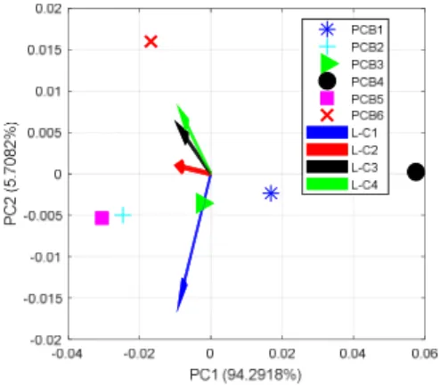
Fig. 11. PCA results for 6 PCBs with one faulty PCB: PCB6; defect case: a
Defect scenario N° 1: One wrong value capacitor
detection:
A data matrix was generated containing a wrong value capacitor C1 inserted in PCB6. After running a PCA on the data, results for both defect cases a and b (see Table 3) show that PCB6 is isolated from the non-faulty PCB cluster. As the calculated PC2 coordinates in both cases is the highest, PCB6 is considered as an outlier, thus, a defected PCB.
For the first case where C1 has a value lower than reference (C1ref=22µF): the projection of the IVs shows that only L-C1, which is the projection corresponding to the first PC in the PC space, points toward the defect plane which is the plane containing the faulty PCB6 (see Fig.11). Contrarily to the second case where C1 has a value higher than C1ref, L-C1 points away from the defect plane (see Fig.12).
Defect scenario N° 2: Two wrong value capacitors
detection:
The IV corresponding to capacitor C4, which has a lower value than the reference, points directly to
the defect plane. L-C1 corresponding to C1, which has a higher value than the reference, points away from this plane (see Fig. 13).
Defected PCBs have always a |PC2| higher than the good PCBs. The plane containing the defected PCBs called the defect plane, is parallel to the plane containing good PCBs. Projected IVs pointing toward this plane correspond to defected capacitors that have a lower value than reference. Those that point away from the defect plane correspond to either wrong value capacitors that have higher values than the reference (see Fig. 11), or non-faulty in-tolerance capacitors (see Fig. 15). The use of PCA allows not only a detection of a faulty PCB, but also the components that might be contributing to this defect. Knowing that an operator must intervene to change the defected components indicated by projected IVs pointing toward the defect plane, a quick check on components corresponding to the other vectors is necessary.
5. Conclusions and perspectives
We presented the possibility of using infrared thermal signatures to diagnose faulty capacitors
Fig. 12. PCA results for 6 PCBs with one faulty PCB: PCB6; defect case b
Fig. 13. PCA results for 6 PCBs with one faulty PCB: PCB6; defect case: c -0.04 -0.02 0 0.02 0.04 0.06 PC1 (97.9576%) -0.015 -0.01 -0.005 0 0.005 0.01 PCB1 PCB2 PCB3 PCB4 PCB5 PCB6 L-C1 L-C2 L-C3 L-C4
Fig. 14. PCA results for 6 PCBs with one faulty PCB: PCB6; defect case: d
Fig. 15. PCA results for 6 PCBs with one faulty PCB: PCB6; defect case: e
contactlessly on a limited physical access PCBA. It can also detect missing and short-circuited components. This approach proposes to overcome the limitations of classical inspection techniques, which are limited to providing only a physical test of certain components mounted on the BUT. This first experimental result demonstrates that infrared thermal signature approach can provide a viable alternative to detect specific component level defects and decrease the number of traditional test points while still provide improved access.
A simple statistical indicator was used initially to compare measured signatures and has given satisfactory results for simple defect cases. It turned to be not significant in complex defect scenarios that may exist in a typical industrial PCBA.
We introduced the use of Principal Component Analysis algorithm to detect defected PCBAs and identify the components responsible of the defect. Using data from Monte-Carlo simulations run on our multi-physics BUT model, demonstrated that this algorithm can give excellent results regarding the detection of the defected PCBAsand the components responsible for their defect.
Thermal testing is a time consuming test method due to the large delays of thermal phenomena which change from a BUT to another, which makes it the main drawback of this approach. The perspectives of this work include:
Detecting more complex assembly defects using a lower inspection time.
The application of this test approach to other types of circuits
Associating the detection method with a machine-learning algorithm allowing a better detection of defects
Acknowledgment
This work was supported by the National Association of Research and Technology (ANRT) and the characterization platform of LAAS-CNRS. References
[1] M. Moganti, F. Ercal, C. Dagli, S. Tsunekawa, “Automatic PCB Inspection Algorithms: A Survey”, Computer Vision and Image Understanding, Vol. 63, No. 2, pp. 287-313, 1996.
[2] J. Sexton, “Infrared Inspection Finds Elusive Faults”, Test & Measurement World, 2001.
[3] M. Vladutiu, H. Moldovan and M. Marcu, “A New Method of Testing Using Infrared Images”, CONTI 2000
[4] Texas Instruments website, Power management products: http://www.ti.com/lit/ds/symlink/tps61088.pdf 2019, (accessed January 2019)
[5] H. Moldovan, M. Marcu and M. Vladutiu, "PCB Testing Using Infrared Thermal Signatures," 2005 IEEE Instrumentationand Measurement Technology Conference Proceedings, Ottawa, Ont., 2005, pp. 1970-1974. doi: 10.1109/IMTC.2005.1604516
[6] J. Altet, A. Rubio, E. Schaub, S. Dilhaire, W. Claeys, "Thermal Testing: Fault Location Strategies", 18th VLSI Test Symposium, p. 189-193, Apr. 2000.
[7] N. El Belghiti Alaoui, A. Boyer, P. Tounsi, A. Viard, “Upgrading In-Circuit Test of high density PCBAs using electromagnetic measurement and Principal Component Analysis”, Journal of Electronic Testing, December 2018, Volume 34, Issue 6, pp 749–762
[8] N. El Belghiti Alaoui, P. Tounsi, A. Boyer and A. Viard, "New testing approach using near electromagnetic field probing intending to upgrade in-circuit testing of high density PCBAs," 2018 IEEE 27th North Atlantic Test Workshop (NATW), Essex, VT, 2018, pp. 1-8. doi: 10.1109/NATW.2018.8388867S.
[9] Flir Systems website, R&D and science products,
https://www.flir.com/globalassets/imported-assets/document/flir-x6570sc-user-manual.pdf 2018, (accessed January 2019)
[10] Flir Systems website, R&D and science products, http://www.nbn.at/fileadmin/user_upload/Vertretungen/FLI R/X6900sc/Datasheets/X6540sc_66701-0101-en-US_A4-1706-nbn.pdf 2017, (accessed January 2019)
[11] Texas Instruments website, Power management products: http://www.ti.com/lit/ug/slvuaf2/slvuaf2.pdf 2015, (accessed January 2019)
[12] Allegro Design Entry CIS (Cadence Design systems, 17.2-2016)
[13] Simsurfing:
https://www.murata.com/eneu/tool/simsurfing/download
[14] Jolliffe, I. T. Principal Component Analysis. 2nd ed., Springer, 2002.