HAL Id: tel-01499920
https://tel.archives-ouvertes.fr/tel-01499920
Submitted on 1 Apr 2017
HAL is a multi-disciplinary open access
archive for the deposit and dissemination of sci-entific research documents, whether they are pub-lished or not. The documents may come from
L’archive ouverte pluridisciplinaire HAL, est destinée au dépôt et à la diffusion de documents scientifiques de niveau recherche, publiés ou non, émanant des établissements d’enseignement et de
Electronic transport and spin control in SiGe
self-assembled quantum dots
Natalia Ares
To cite this version:
Natalia Ares. Electronic transport and spin control in SiGe self-assembled quantum dots. Quantum Physics [quant-ph]. Université de Grenoble, 2013. English. �NNT : 2013GRENY060�. �tel-01499920�
TH `
ESE
Pour obtenir le grade de
DOCTEUR DE L’UNIVERSIT ´
E DE GRENOBLE
Sp ´ecialit ´e : Nanophysique
Arr ˆet ´e minist ´eriel : 23 avril 2009
Pr ´esent ´ee par
Natalia Ares
Th `ese dirig ´ee parFranc¸ois Lefloch et Silvano De Franceschi
pr ´epar ´ee au sein duLaboratoire de
Transport ´Electronique Quantique et Supraconductivit ´e
et de l’ ´ecole doctoralede Physique de Grenoble
Electronic transport
and spin control in SiGe
self-assembled quantum dots
Th `ese soutenue publiquement le24 octobre 2013,devant le jury compos ´e de :
Julia S. Meyer
Prof., Universit ´e Joseph Fourier Grenoble, Pr ´esident
Seigo Tarucha
Prof., University of Tokyo, Rapporteur
Andreas Fuhrer
Dr., IBM Zurich Research Laboratory, Rapporteur
Yuli V. Nazarov
Prof., TU Delft, Examinateur
Silvano De Franceschi
HDR, CEA Grenoble, Directeur de th `ese
Franc¸ois Lefloch
Acknowledgements
To begin with, I would like to thank the reviewers of this thesis, Dr. Andreas Fuhrer and Prof. Seigo Tarucha, as well as the other honourable members of the jury; Prof. Julia S. Meyer and Prof. Yuli V. Nazarov.
Furthermore, the realization of this work would not have been possible without the immense support of many people. In the first place, I would like to thank Silvano De Franceschi and Georgios Katsaros for their guide and patience during these years. Silvano has been an inspiring source of exciting ideas and Georgios, a indefatigable guide through each step towards the actual realization of these.
I would also like to thank Aaron Prager and Eduardo Lee for their always at hand help and advise, and for the many pleasant moments shared at the lab. I want to thank Elena Talache-Prager and Isil Aydin too, for their warmth and caring.
For the support I have been given at the beginning, I would like to mention Massimo Mongillo et Panayotis Spathis and for the last few months, Juan Carlos Estrada, Patrick Torresani and Julien Renard.
Finally, I would like to thank Vitaly Golovach for the production and constant enlightenment of all the theoretical work presented in this thesis.
Bien que je n’ai pas appris plus que quelques mots, je voudrais remercier certaines personnes en fran¸cais. Premi`erement, `a Fran¸cois Lefloch, pour son ´enorme patience, ses attentions, et surtout pour sa qualit´e humaine incom-parable.
`
A Jean-Luc Thomassin, Frederic Gustavo, Christophe Lemonias, Frederic Poletti, Iulian Matei et Jean-Michel Martinod, pour faire de la ‘magie’ et pour ˆetre toujours prˆet `a m’aider. Et finalement `a Georg Knebel, Christophe Marcenat, Louis Jansen, Claude Chapelier, Xavier Jehl, Laurent Vila, Marc Sanquer et Jean-Pascal Brison pour leur ´enorme soutien et `a Benoit Voisin, Benoˆıt Roche, Andreas Pfeffer, Charl`ene Tonnoir, Alexander Grimm, Toai Le Quang, Paul Clapera, Soumya Ray, Mathieu Taupin et Audrey Grockowiak, parmi beaucoup d’autres camarades, pour leur compagnie.
cari˜no, contenci´on y apoyo incondicional. Por hacerme sentir que 10.000 km no son nada y por perdonar tantas ausencias. Especialmente a mi mam´a, por ponerme siempre primero y por el esfuerzo y las l´agrimas puestas en dejarme ir. A mi hermana, por su infinita capacidad para quererme y mimarme. Y
a mi nonna, por ser desde siempre mi fan n´umero uno. Quiero mencionar
tambi´en a Naty, por estar siempre dispuesta a rescatarme a donde quiera que vaya, a mis t´ıos y a mi nonno, por quererme tanto, a Cami, a Patri y
tambi´en a las ´ultimas adquisiciones, Marcelo, Mart´ın y Carlos.
A Elisa Chisari, Ariel Berenstein, Ezequiel Badgen, Nahuel Vega y Mari-cel Repetto por cuidar nuestra amistad a pesar de la distancia. Gracias por estar siempre para m´ı.
A mi familia pol´ıtica, Mercedes, Luc´ıa, Pablo, Clara, Alberto y Alejandra
y Ricardo, por el gran cari˜no que me brindan.
Y para terminar, a Mart´ın Obligado por ser mi incondicional compa˜nero,
sost´en en los momentos m´as dif´ıciles. Vos hiciste que todo esto fuera posible. Gracias, gracias, gracias,
Introduction
La m´ecanique quantique affiche d´ej`a toute son ´etranget´e en consid´erant l’´equation de Schrdinger dans un puits de potentiel `a une dimension. L’effet tunnel qui en r´esulte, en est un exemple frappant. La possibilit´e de r´ecr´eer cette situation dans un syst`eme mat´eriel est un enjeu excitant et un grand pas vers le contrˆole des effets quantiques. Par exemple, il est maintenant possible de confiner des ´electrons dans des dispositifs semi-conducteurs per-mettant une technologie de cellules solaires plus efficaces.
Le confinement spatial des spins ´electroniques a ´et´e sugg´er´e comme une approche possible pour la r´ealisation d’un ordinateur quantique. Chaque spin formant un syst`eme `a deux niveaux pouvant coder une bit ´el´ementaire pour l’information quantique (spin qubit). Cette proposition par Loss et Di Vincenzo a contribu´e `a l’ouverture d’un domaine de recherche important d´enomm´e spintronique quantique. L’int´erˆet des qubits de spin s’appuie sur le fait que les ´etats de spin ont des temps de coh´erence beaucoup plus long que les qubits de charge (´etats orbitaux).
Un potentiel de confinement de spin peut ˆetre cr´e´e de diff´erentes fa¸cons comme en appliquant `a la fois un champ magn´etique et un champ ´electro-statique, par l’application de champs ´electriques alternatifs ou encore `a l’inter-face entre diff´erentes couches d’oxydes conducteurs. L’utilisation de l’aligne-ment des bandes d’´energies de semi-conducteurs de diff´erentes natures permet ´egalement de cr´eer un potentiel de confinement. Cependant, les dimensions spatiales du syst`eme obtenu doivent toujours ˆetre inf´erieures `a la longueur de coh´erence de phase des quasi-particules consid´er´ees afin de pr´eserver leur comportement quantique.
Jusqu’`a pr´esent, la plupart des progr`es ont ´et´e r´ealis´es en utilisant des h´et´erostructures semiconductrices `a base d’arsenure de Gallium (GaAs). Dans de tels syst`emes, le mouvement des porteurs de charges est limit´e `a un plan bidimensionnel et le confinement lat´eral peut ˆetre obtenu par des techniques de lithographie jusqu’`a des tailles inf´erieures `a 100 nm. De cette fa¸con, des syst`emes quasi-z´ero-dimensionnels dont les ´etats ´electroniques sont parfaite-ment quantifi´es (boˆıtes quantiques), sont r´ealis´es.
Diverses techniques utilisant des signaux hautes fr´equences ont permis de manipuler et lire l’´etat de spin de tels boˆıtes quantiques de GaAs et, il y a quelques ann´ees, les premiers qubits de spin ont ´et´e d´emontr´es. Cependant, ces syst`emes ont montr´e des temps de coh´erence relativement courts en raison de l’interaction hyperfine avec les spins nucl´eaires du Gallium et de l’Arsenic. En d´epit de progr`es significatifs sur le contrˆole de la polarisation, ce probl`eme n’est toujours pas r´esolu.
Au cours de ces derni`eres ann´ees, un effort croissant s’est donc concentr´e sur des syst`emes `a base de mat´eriaux alternatifs pour lesquels l’interaction hyperfine est naturellement absente ou rendue tr`es faible par des techniques de purification. Mˆeme si le Silicium, qui est le mat´eriau de base en mi-cro´electronique, remplit cette condition, il souffre d’une faible mobilit´e par rapport aux semiconducteurs III-V ce qui pose probl`eme pour la spintron-ique quantspintron-ique. Les structures `a base Silicium-Germanium (SiGe) offrent un moyen de contourner ce probl`eme tout en gardant un mat´eriau compatible
avec les proc´ed´es de fabrication standards 1.
Durant mon travail de th`ese, je me suis concentr´ee principalement sur l’´etude des propri´et´es ´electroniques d’ˆılots auto-assembl´es (nanocristaux) de SiGe. Le manuscrit de th`ese qui relate les principaux aspects de cette ´etude est organis´e en six chapitres. Dans le premier chapitre, je d´ecris les principaux concepts de la croissance cristalline d’ˆılots auto-assembl´es de SiGe ainsi que les propri´et´es du potentiel de confinement qu’ils d´efinissent. Le chapitre 2 est consacr´e aux principes du transport ´electronique dans de telles structures. Le chapitre 3 traite de la modulation ´electrique du facteur de Land´e (g) des trous confin´es dans les ˆılots en vu de la manipulation rapide des ´etats de spin. Dans le chapitre 4, je pr´esente les r´esultats th´eoriques et exp´erimentaux relatifs `a la s´electivit´e en spin dans les nanocristaux de SiGe. Le chapitre 5 d´ecrit les r´esultats sur la r´ealisation d’une pompe ´electronique obtenue `a partir de nanofils d’InAs/InP. Enfin, le chapitre 6 montre les progr`es technologiques que j’ai obtenus vers la r´ealisation et l’´etude de dispositifs coupl´es `a base de nanocristaux de SiGe.
1
R´
esum´
e
Le Silicium (Si) et le Germanium (Ge) sont des semi-conducteurs miscibles dans tout le domaine de composition. Les deux mat´eriaux ont une structure cristalline de forme diamant mais leurs param`etres de maille sont diff´erents:
5.43 ˚A pour le Si et 5.66 ˚A pour le Ge. Dans une premi`ere phase de
crois-sance, le Ge pousse en couches minces sur un substrat de Si (100). A cause du d´esaccord de param`etres de maille entre les deux mat´eriaux une con-trainte biaxiale se construit et est lib´er´ee `a partir de 3-4 couches atomiques. Cette relaxation de contrainte se fait soit par l’´etablissement de dislocations, soit par la formation de structures cristallines 3D appel´ees ˆılots (croissance Stranski-Krastanov).
Les nanostructures form´ees peuvent avoir une vari´et´e de tailles et de formes en fonction des param`etres de croissance. Dans cette th`ese, je me suis int´eress´ee essentiellement aux ˆılots en forme de dˆome. Ces ˆılots ont une structure cristalline et des dimensions (∼ 100 nm) accessibles par les moyens actuels de nanofabrication. En fonction de l’alignement des bandes de con-duction et de valence un potentiel de confinement pour les trous peut ˆetre cr´e´e (chapitre 1).
Afin d’´etudier les propri´et´es de transport ´electronique, il est n´ecessaire de pouvoir contacter ´electriquement ces ˆılots. La technique g´en´eralement utilis´ee et dont la mise au point a ´egalement fait partie de mon travail de th`ese, consiste `a utiliser des proc´ed´es de nanofabrication pour d´eposer sur ces ˆılots plusieurs contacts m´etalliques (source, drain et grille). Les contacts drain et source permettent de connaitre la r´eponse ´electrique du syst`eme alors que la tension de grille offre la possibilit´e de r´egler les niveaux d’´energie dans l’ˆılot. Les premi`eres mesures de transport ´electronique obtenues par le groupe sont r´esum´ees dans ce manuscrit (chapitre 2) ce qui permet de d´ecrire et de d´etailler les concepts g´en´eraux de la physique sous-jacente aux syst`emes que j’ai ´etudi´es: spectres d’´energie discrets, couplage spin-orbite, anisotropie du facteur de Land´e, effet du champ magn´etique, etc.
Durant ma th`ese, j’ai contribu´e `a la mise au point d’une ´etude exp´erimen-tale de r´esonance de spin ´electronique (ESR). Cette technique consiste `a
ma-nipuler de mani`ere coh´erente l’´etat de spin des ´electrons grˆace `a un champ radio-fr´equence. Les techniques habituelles consistent `a placer le syst`eme dans un champ magn´etique statique et d’appliquer un champ magn´etique alternatif perpendiculaire au champ statique pour exciter et manipuler les spins. Dans notre cas, le champ magn´etique radio-fr´equence est remplac´e par un champ ´electrique et la modulation du facteur de Land´e permet d’exciter les spins ´electroniques. Mon travail a permis l’observation exp´erimentale d’une modulation exceptionnelle et non-monotone du facteur de Land´e dans ces ˆılots de SiGe (chapitre 3). Pour interpr´eter ces r´esultats, nous proposons un nouveau m´ecanisme appliqu´e `a un syst`eme de trous `a basse dimension-nalit´e. Ce m´ecanisme repose sur l’existence d’un terme de correction impor-tant dans le facteur de Land´e et ignor´e jusqu’ici. Nous montrons ´egalement que l’amplitude de cette correction d´epend du m´elange des trous lourds et l´egers qui composent la fonction d’onde ´electronique.
L’´etape compl´ementaire `a la manipulation coh´erente des spins ´electro-niques, est la d´etection de leur ´etat. Une technique appel´ee conversion spin-charge permet de corr´eler les ´etats de spin aux ´etats de spin-charge. Ainsi, une mesure ´electrique de la charge d’une boˆıte quantique permet de connaitre l’´etat de spin. Plusieurs m´ethodes de d´etection ont d´ej`a ´et´e d´emontr´ees exp´erimentalement. La premi`ere exploite la diff´erence d’´energie entre les deux ´etats de spin et une deuxi`eme profite de la diff´erence de taux tunnels des ´etats de spin vers les ´electrodes m´etalliques. Dans le chapitre 4, ces diff´erentes m´ethodes sont rappel´ees et je discute une autre m´ethode bas´ee sur le couplage spin-orbite propre aux syst`emes de trous des ˆılots de SiGe.
Les pompes `a ´electrons sont couramment r´ealis´ees dans des syst`emes nanom´etriques. La s´electivit´e en spin du taux tunnel ´evoqu´e au chapitre 4, permet d’envisager la r´ealisation d’une pompe ´electronique en manipu-lant l’´etat de spin d’une boˆıte quantique. La simple manipulation-rotation du spin permet de g´en´erer un courant `a travers la nanostructure sans ap-pliquer de tension source-drain. Durant ma th`ese, j’ai fabriqu´e et ´etudi´e un tel syst`eme `a partir de nanofils d’InAs/InP. Les d´etails de cette ´etude sont pr´esent´es dans le chapitre 5.
Enfin, le chapitre 6 est enti`erement d´edi´e aux nombreux efforts tech-nologiques d´evelopp´es durant mon travail de th`ese pour aller plus loin dans la r´ealisations de nanostructures complexes `a partir de plusieurs ˆılots de SiGe connect´es. Pour ce faire, j’ai du mettre au point un nouveau protocole tech-nologique qui permet d’adresser individuellement plusieurs ˆılots et cela de mani`ere contrˆol´ee. Des g´eom´etries diverses et vari´ees sont pr´esent´ees ainsi que les enjeux scientifiques associ´es.
Conclusion
En plus des applications potentielles, les boites quantiques semi-conductrices sont des syst`emes mod`eles pour ´etudier de nombreux ph´enom`enes quantiques. Dans ce manuscrit de th`ese, j’ai pr´esent´e des mesures exp´erimentales et des mod`eles qui ouvrent des perspectives nouvelles sur les potentialit´es de ces nanostructures pour le transport ´electronique quantique. Ces ´etudes ont prin-cipalement port´e sur les nanocristaux de SiGe obtenus par croissance auto-assembl´ee pour lesquels un long temps de coh´erence de spin est pr´edit. Mon travail a permis de d´ecrire les effets de confinement ´electrostatique et r´ev´eler des effets de tunneling/cotunneling et d’explorer les divers ph´enom`enes li´es aux ´etats de spin des porteurs de charge.
Durant ma th`ese, j’ai pu mesurer le tenseur de Land´e des trous dans des ˆılots de SiGe et montr´e qu’il est possible de moduler sa valeur par un champ ´electrique externe. L’analyse d´etaill´ee des r´esultats a montr´e que cet effet ne peut pas ˆetre li´e `a un gradient de concentration dans l’ˆılot. Nous avons alors propos´e une interpr´etation nouvelle bas´ee sur la prise en compte d’un terme correctif dans l’expression du facteur de Land´e et g´en´eralement n´eglig´e dans la litt´erature.
Ces nanocristaux de SiGe permettent ´egalement d’envisager la manip-ulation des ´etats de spin par un champ ´electrique radio-fr´equence. Mon travail de th`ese a permis de clarifier les conditions dans lesquelles il est pos-sible d’utiliser ces boˆıtes quantiques en SiGe comme brique ´elementaire pour l’information quantique bas´ee sur le codage des ´etats de spins. Les esti-mations montrent qu’il doit ˆetre possible d’obtenir des temps de coh´erence comparables `a ceux obtenus dans les nanofils d’InSb.
Par ailleurs, en ´etudiant les processus de transfert ´electronique in´elastique dans ces boˆıtes quantiques, j’ai pu montrer une asym´etrie de conductance en fonction de l’´etat de spin. Cette observation nous a amen´e `a proposer un protocole exp´erimental qui permet de fabriquer une pompe ´electronique d’une toute nouvelle nature. Pour des raisons de difficult´es dans les processus de nanofabrication, j’ai r´ealis´e cette pompe `a partir de fils semi-conducteurs d’InAs/InP.
Enfin, j’ai d´evelopp´e une m´ethode originale de nanofabrication afin de pouvoir fabriquer `a la demande des nanostructures incluant plusieurs ˆılots de SiGe auto-assembl´es et donc al´eatoirement dispers´es sur une substrat de Sili-cium. Ces avanc´ees technologiques ouvrent des perspectives pour l’ing´enierie quantique bas´ee sur ce genre de mat´eriau qui est compatible avec les tech-niques de fabrication modernes en micro-nano´electronique.
Contents
Introduction 1
1 SiGe self-assembled nanostructures 3
Properties of the confinement potential and the sporbit
in-teraction in SiGe islands . . . 6
2 Single quantum dot devices based on SiGe self-assembled nanostructures 10 2.1 Device fabrication . . . 10
Fabrication of SiGe nanodevices . . . 11
2.2 Low-temperature setups . . . 18
2.3 Tunneling and cotunneling spectroscopy . . . 20
2.3.1 Basics of charge transport . . . 20
2.3.2 Elastic and inelastic cotunneling processes . . . 24
2.4 First hybrid devices on SiGe self-assembled quantum dots . . . 24
2.5 Hole g-factor measurements in SiGe self-assembled nanostruc-tures . . . 26
3 Electrically tunable g-factor 32 3.1 Device description . . . 33
3.2 Experiment . . . 33
3.3 Analysis . . . 36
3.4 Electrically tunable g-factor as a control mechanism . . . 47
4 Spin selective tunneling 52 4.1 Experiment . . . 53
4.2 Analysis . . . 56
5 A Rabi electron pump 61 5.1 Device description . . . 63
5.3 Discussion . . . 70
6 Coupled SiGe self-assembled quantum dots 73 6.1 Directed approach . . . 76
Difficulties and remedies . . . 83
6.2 First transport measurements on double-dot devices . . . 91
Transport mediated by a metallic bridge . . . 92
Conclusion 101
Introduction
Quantum mechanics displays all its exciting strangeness already by consid-ering the Schr¨odinger equation in a one-dimensional square-well potential; tunneling events put this statement in evidence. To recreate this situation in a given material system is an inspiring playground and a big step towards taking control of quantum mechanisms. For instance, it is now possible to confine electrons in solid-state devices enabling a more efficient solar-cell technology.
Confining individual electron spins has in fact been suggested as a possible approach to the realization of a quantum computer. Each electron spin forms a natural two-level system encoding an elementary bit of quantum information (a so-called spin qubit). This proposal, by Loss and DiVincenzo [1], has contributed to the opening of an active research field referred to as quantum spintronics. Spin qubits rely on the fact that spin states can preserve their coherence on much longer time scales than charge (i.e. orbital) states.
A confinement potential can be created artificially in many different ways; producing constant magnetic fields and spatially inhomogeneous elec-tric fields, applying oscillating elecelec-tric fields, using conductive oxide layers, etc. To take advantage of the band-alignment of different semiconductors is among these. The relevant dimensions of the considered system should still be smaller than the phase coherence length of the confined particles in order that their quantum behaviour is preserved.
So far, most of the progress has been achieved using GaAs-based semi-conductor heterostructures [2]. In such layered systems the motion of carri-ers is confined to a plane and further confinement is achieved by means of lithographic techniques, which allow lateral confinement to be achieved on a sub-100 nm length scale. In this way, quasi-zero-dimensional systems whose electronic states are completely quantized, i.e. quantum dots (QDs), can be devised.
Various time-resolved techniques involving high-frequency electrical sig-nals have been developed to manipulate and read-out the spin state of
con-fined electrons in GaAs QDs, and several years ago the first spin qubits were reported [2]. In GaAs-based QDs, however, the quantum coherence of electron spins is lost on relatively short time scales due to the hyperfine interaction with the nuclear spins (both Ga and As have non-zero nuclear spin). In spite of significant advances in controlling the nuclear polarization [3, 4], this problem remains unsolved.
In the past few years an increasing effort is concentrating on alternative material systems in which hyperfine interaction is naturally absent or at least very weak and, in principle, controllable by isotope purification.
While Si fulfills this requirement and it is the dominant material in mod-ern microelectronics [5], it suffers from low mobility compared to III-V semi-conductors, which obstructs its application for quantum spintronics. SiGe structures offer a way to circumvent this problem that is still compatible with
standard silicon processes 2.
I have focused mainly on the study of the electronic properties of SiGe self-assembled islands, also called SiGe nanocrystals. This work, which con-densates the main points of this study, is organized as follows; in the first chapter, I describe the basics of the growth of SiGe self-assembled islands and the properties of the quasi-zero-dimensional confinement potential that they define. Chapter 2 is devoted to the basics of electronic transport in these structures. Chapter 3 deals with the electric modulation of the hole g-factor in SiGe islands, which would enable a fast manipulation of the spin states. In Chapter 4 I present theoretical and experimental findings related to spin selectivity in SiGe QDs and Chapter 5 is dedicated to the realization of an electron pump in InAs nanowires based on this effect. Finally, Chapter 6 exhibits our progress towards the study of coupled SiGe QD devices.
2
Chapter 1
SiGe self-assembled
nanostructures
Molecular Beam Epitaxy (MBE) is a growth technique by which a single crystalline film of a given material can be grown on a crystal substrate un-der ultra-high vacuum conditions. Among other material combinations, this technique enables the growth of crystalline Ge on a Si(001) wafer.
Si and Ge are semiconductors of the group IV, miscible over the
en-tire composition range. Si1−xGex alloys from x = 0 to x = 1 can thus be
grown. Both Si and Ge have a diamond-like crystal structure, but their
lat-tice constants (α) are different; αSi = 5.43˚A while αGe = 5.66˚A. Initially
Ge grows on Si(001) in a layer-by-layer mode, but as the in-plane lattice-constant of Ge has to adjust that of Si, a biaxial stress is built up. After 3 or 4 monolayers, the accumulated strain is released either through the for-mation of dislocations or through the forfor-mation of crystalline 3D structures, usually called islands. This is the so-called Stranski-Krastanov growth mode [7, 8]. Schematic representations of the growth mode and the strain relax-ation mechanism are shown in Fig.1.1 a) and b), respectively. Finally, these so-called self-assembled structures are capped with a thin Si layer of about 2 to 4 nm. This Si cap prevents the formation of Ge oxides, which are known to be highly soluble in water and thermally unstable.
The formed nanostructures can have a variety of sizes and shapes depend-ing on the chosen growth parameters (see Fig.1.2) [9, 10]. Unless specifically mentioned, from now on I will focus on dome islands. These islands, while crystalline, have accessible dimensions for the current sample fabrication ca-pabilities.
It has been shown that the position of these nanocrystals can be controlled by prepatterning the growth surface [14, 15]. An example of this prepatterned
a)
b)
Figure 1.1: a) Schematic of the evolution of the growth of Ge islands on Si by means of the Stranski-Krastanov growth mode, from [11]. b) Schematic representation of the strain relaxation by formation of a 3D island. Taken from www.fkf.mpg.de/mbe/.
pyramid
hut
dome
superdome
50x50x7 nm3 50x50x10 nm3 50x32x3 nm3 110x110x27 nm3Figure 1.2: Three-dimensional Scanning Tunneling Micrographs (STM) of self-assembled SiGe nanocrystals with characteristic ‘pyramid’, ‘hut’, ‘dome’ and ‘superdome’ shapes. Taken from [11]. Inset: Cross sectional Trans-mission Electron Microscopy (TEM) image of a dome island. Taken from [12].
Figure 1.3: Atomic force micrograph (4.7 × 4.7) µm2 illustrating a
self-organized array of SiGe nanocrystals grown on a prepatterned silicon wafer [13].
be a platform for integrated circuits compatible with CMOS technology [16].
Properties of the confinement potential and
the spin-orbit interaction in SiGe islands
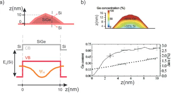
Depending on the relative position of the conduction and the valence band of two semiconductor materials, type I and type II alignments are defined. It has been shown that a type II alignment is present for strained SiGe on Si [17]. In this case, the conduction and the valence band align in such a way that a confinement potential for holes is created. In Fig.1.4 a) (TOP) a SiGe dome island with a simplified compositional cross-section is represented together with its correspondent schematic band-alignment, Fig.1.4 a)(BOTTOM).
For SiGe the valence band varies linearly with the Ge content [18], which is a function of the crystal height (z) [19]. Figs.1.4 b) (TOP) and (BOTTOM) show the dependence along z of the Ge content of a dome island. To sum up, we can say that holes are confined in a quasi-one-dimensional potential with a shape that is given by the compositional gradient of the SiGe island. Noteworthy, holes in the valence band have an orbital angular momen-tum l = 1. Given the multiplicity, (2l + 1), this band is threefold degenerate (sixfold degenerate taking into account the spin). However, because of the confinement and compressive strain in the islands, this degeneracy is lifted giving rise to heavy-holes (HH) and light-holes (LH) branches, with projec-tions of the orbital angular momentum m = ±1 and m = 0, respectively. In the QD, the orbital states consist of a mixture of HH and LH wave functions. When spin-orbit (SO) interactions are considered, the orbital angular
momentum couples to the spin degree of freedom s = 1
2. The conserved
magnitude is now the total angular momentum J that can take the values
J = 32 and J = 12. Those corresponding to J = 32 are the HH and LH bands,
with m = ±3
2 and m = ±
1
2 respectively. The so-called split-off band is the
one corresponding to J = 12 and its energy separation from the heavy- and
light-hole bands, called spin-orbit splitting (∆SO), quantifies the strength of
the SO interaction. Fig.1.5 illustrates this split-off band as well as the HH and a LH branches, whose Gamma-point degeneracy is lifted by strain and confinement. It should be noted that the effective masses of confined holes are dependent on directions. The effective mass of HH branches along the quantization axis is larger than that of LH branches, while the effective mass of HH branches on the xy-plane is smaller than that of LH branches.
The SO interaction has become of central interest for the possibility to perform electrically-driven spin manipulation. Golovach et al. [21] have
pro-b) a) E (Si)g Si Si SiGe yH z(nm) CB VB z(nm) Si SiGe Si 0 10 0 10 z(nm) z(nm)
Figure 1.4: a) TOP: scheme of a nanostructure with a simplified composi-tional cross-section. BOTTOM: corresponding conduction band (CB) and
valence band (VB) alignment scheme, where Eg(Si) is the Si band-gap and
Ψh represents the localization of holes. b) TOP: Chemical composition map
of dome islands [20]. BOTTOM: Ge content (line) of these islands as a function of z. The lattice parameter relaxation with respect to the lattice parameter of Si, ∆a/a, is also displayed (points). Taken from ref.[19].
k
x
,k
y
! !
E
D
zD
SOHH
LH
SO
Figure 1.5: Qualitative band diagram of a Ge-rich SiGe quantum well, with
E the energy and kx and ky the plane wave vectors. The HH and a LH
branches are lifted by ∆z due to the presence of strain and confinement and
they anticross at finite kx or ky. A split-off band appears as a result of the
posed an all-electrical approach, called electric-dipole spin resonance (EDSR), that was successfully used for spin rotations of electrons in QDs [22, 23].
In the case of Si, ∆SO = 44 meV, whereas for Ge ∆SO = 290 meV.
There-fore, SO effects in Si quantum structures are rather small and SiGe appears again as a better candidate for quantum spintronics. Furthermore, valence band states have a stronger SO coupling than the conduction band states, which makes hole confinement very promising for an efficient electric manip-ulation of the spin states. To conclude, holes confined in SiGe structures have very propitious properties for the realization of fast spin qubits.
Chapter 2
Single quantum dot devices
based on SiGe self-assembled
nanostructures
In order to perform a transport-spectroscopy study of the electronic prop-erties of SiGe nanocrystals, metal electrodes serving as source and drain contacts are required. These contacts are metal-like reservoirs to which an
external bias voltage Vsd can be applied. By measuring the current flow
through this device, the electronic properties of carriers in the crystal can be explored. Fig.2.1 a) illustrates these kind of devices based on SiGe islands.
In addition, a gate voltage (Vg), a voltage applied to an additional metallic
electrode, gives the possibility to electrically tune the energy levels and hence influence the current that flows through a device.
In order to have a clear picture of the processes involved in the trans-port of carriers, the literature often refers to schemes like the one shown in Fig.2.1 b). In this scheme, the source and drain contacts are symbolized by
their electrochemical potentials µs and µd, with |µs − µd| = eVsd where e
is the absolute value of the elementary charge. A one-dimensional square well potential represents the SiGe nanocrystal. As discussed in the previous chapter, this is a fairly adequate picture although the quasi-zero-dimensional confinement that defines the QD in the crystal is created in the valence band and consequently, the carriers are holes instead of electrons.
2.1
Device fabrication
The nanodevices were fabricated using electron-beam (ebeam) lithography. The basic process flow for this techniques is illustrated in Fig.2.2. The first
source
drain
a)
b)
V
geV
sdm
Sm
d source drainFigure 2.1: a) Schematics of a SiGe nanocrystal based device. b) Schematics
of a device, µs and µd being the electrochemical potentials of the metallic
contacts and Vsd, the bias voltage between them. The gate voltage Vg
regu-lates the current flow through the device by electrically tuning the quantized states inside the crystal.
step is to deposit an organic resist material onto a substrate by means of a spinner. The resist is then selectively exposed to an electron beam. The beam induces changes in the chemical structure of the irradiated polymer, such that in a following step the irradiated portion dissolves when immersed in a developer (positive resist). Once the pattern is defined on the substrate, a given metal is evaporated and it covers the resist profile. Finally, the resist is removed from the substrate through a so-called lift-off process and just the metal deposited on the pattern remains.
Fabrication of SiGe nanodevices
Inspired by recent work on self-assembled InAs nanocrystals [24, 25, 26], a technique to contact single SiGe islands has been developed by the group. It starts from a wafer of SiGe nanocrystals grown on a non-standard silicon-on-insulator (SOI) substrate, which consists of an undoped silicon overlayer, a
SiO2 insulating layer, and a degenerately doped silicon substrate that serves
as a back-gate 1(Fig.2.3 a)).
1
These substrates were fabricated by F. Fournel in CEA, LETI, from commercial SOI wafers. These commercial wafers were thermally oxidized and bonded to a heavily doped Si wafer. By grinding and selective chemical etching, non-standard SOI substrate having
a)
b)
c)
d)
e)
f)
Figure 2.2: Nanofabrication technique based on ebeam lithography; a) design of the two lines which represent the desired pattern to be transferred, b) substrate coated with a resist material, c) the resist is selectively exposed to the electron beam, d) after development the exposed parts of the resist dissolve, e) a metal is evaporated, f) the resist and the residual metal are removed by immersing the substrate in a solvent (lift-off process).
b) 100 mm d) c) a) e) f) Si SiO2 heavily-doped Si Vbg Vsd source/drain Al AlO2 Ti/Au
linking pad Ti/Au
to write-field electrode
Figure 2.3: a) Scheme of a contacted SiGe self-assembled nanostructure grown on a non-standard SOI wafer. This wafer consists of a thin Si layer,
a SiO2 layer of about 65 nm and a heavily doped silicon substrate. To this
doped substrate, a voltage Vbg can be applied in order to gate the SiGe
de-vices. b) Pattern that defines the write-fields and the alignment crosses on the substrate in the first step of ebeam lithography. c) Design of the source and drain contacts distributed all over the inner area of a particular write-field in the second step of ebeam lithography. Numbers are added to the side of each pair of contacts in order to be able to address later those which contact a SiGe island. d) SEM image of source and drain contacts after expo-sure, etching and metal deposition. An island is contacted by these leads. e) The third step of ebeam lithography connects those pairs of electrodes that contact a SiGe crystal to the write field electrodes. f) Ti/Au linking pads used to contact the aluminium leads from its bottom surface in order to get
a good electrical contact that is otherwise prevented by the AlO2 formation.
a)
b)
c)
layer 1 layer 2
substrate
Figure 2.4: a) Double layer resist spun on a substrate, the molecular weight of the top layer being higher than the one of the bottom layer. b) Same bilayer after exposure. c) Same bilayer after exposure and development. This resist profile is known as undercut.
Following the procedure described in Fig.2.2, a first step of ebeam lithog-raphy is done on this wafer in order to define the pattern shown in Fig.2.3 b). It consists of a set of alignment crosses and 4 write-fields, each of them
with 16 electrodes that shrink until they frame an area of 250 × 250 µm2.
The source and drain contacts are defined in this area, shown in Fig.2.3 c), in a second step of ebeam lithography. A big number of contacts increases the probabilities to actually catch a SiGe island in between.
This second step of ebeam lithography is not as trivial as the first one; firstly, because it will define the contact surface of the metal with the semi-conductor island and secondly, because the source and drain contacts should be separated by a ∼ 20 nm gap in order to contact a SiGe island. There-fore, an exhaustive list of the parameters chosen for this fabrication step is essential, and thus it is displayed below.
1. Resist
A bilayer technique, in which a high molecular weight resist is spun on top of a low molecular weight resist was used. The sensitivity of a resist is related to its molecular weight; at low molecular weights, high sensitivities, which means that lower doses of radiation will be needed in order to secure a proper exposure. Consequently, the effective dose of radiation delivered to the bottom layer (more sensitive) will be bigger than the one delivered to the top layer (less sensitive). This difference in sensitivity results, after development, in a particular resist profile called undercut (see Fig.2.4). This resist profile makes the lift-off process easier, especially for narrow gaps.
The bottom layer was chosen to be PMMA 4% 200K and the top layer, PMMA 2% 950K. The top layer is most critical, as it is the one that limits the resolution. PMMA 2% was chosen for its capability of producing reduced thickness layers that allowed us to achieve the resolution needed in the pattern writing.
In order to guarantee a total resist thickness of about 200 nm, both resist layers were spin coated for 30 s at a speed of 6000 rpm and an acceleration of 2000 rpm/s. Then, they were heated, one at the time,
at 180◦C for 5 min in order to secure the evaporation of the solvents
that are present in resist materials. 2. Exposure
Ebeam lithography can be performed with relatively simple modifica-tion to a convenmodifica-tional scanning electron microscope (SEM) through computer control of the position of the beam. We had access to a equipment of this kind, called modified SEM, that is capable of defin-ing features with critical dimensions of the order of 100 nm and that has an alignment precision, with respect to a set of predefined crosses, in the order of 250 nm. Noteworthy, this value varies significantly with
the chosen write-field area ((250 × 250) µm2 in this case). The
ac-celeration voltage was 20 kV and the current of the electron beam 15 pA.
3. Development
To develop the exposed resist, a 30 s dip in a solution MIBK/IPA 1 : 3 followed by a 1 min rinse in IPA was performed. MIBK (Methyl Isobutyl Ketone) itself provides the ingredient necessary for solubility control and swelling of the resist, while the IPA (Propan-2-ol) stops the development. Solutions containing a higher amount of IPA are best for high resolution fabrication.
4. Etching
As discussed in the previous chapter, the SiGe nanocrystals are capped with a thin Si layer of 2 to 4 nm. Once exposed to air under ambient conditions, a very shallow layer (approximately 1 nm) of so-called na-tive oxide is formed on the surface. This silicon dioxide represents a huge tunnel barrier for carriers and, consequently, it should be removed in order that current can flow through the device. This is the reason why a 10 s wet etching in BHF (Buffered Hydrofluoric acid) followed by a short rinse in deionized water was performed before the metal
BHF refers to a mixture of a buffering agent, such as ammonium
fluo-ride (NH4F), and hydrofluoric acid (HF). Concentrated HF (typically
49% HF in water) etches silicon dioxide too quickly for good process control. For that reason, BHF is commonly used for more controllable etching, as it can keep the etch rate low and constant.
This solution etches the native silicon oxide in a few seconds and it is self-limited, i.e. once the silicon oxide is etched away, due to its high selectivity, the Si left in the capping layer (∼ 1 to 3 nm) is not attacked. In addition, this Si layer becomes hydrogen passivated, which means that its oxidation when exposed again to air is prevented for a limited time.
5. Metal deposition
While the capping layer is still hydrogen passivated, the deposition of a metallic layer should take place. This is done with an electron beam
evaporator, with a base pressure of 1 × 10⁻⁸ mTorr.
The electron beam is generated by thermal emission from a heated tungsten filament. A crucible containing the material to be deposited is held at a positive potential relative to this filament. To avoid chem-ical interactions between the filament and the crucible material, the filament is kept out of sight. Magnetic and electric fields are then em-ployed to direct and steer the electron beam from its source to the crucible location. One can choose between different materials to be evaporated by rotating the crucible selector.
In order to improve the uniformity of the evaporated layer and to avoid the overheating of the resist, the substrate stage is located far away from the source and it rotates during deposition.
Under these conditions, a layer of 30 nm of Al is deposited to form the source and drain contacts.
6. Lift-off
The remaining resist is lifted in hot acetone (40◦C) for 5 min. Before
removing the sample from the acetone bath, the metal layer is peeled off by gently forcing with a pipette the liquid towards the substrate surface. Finally, the sample is sprayed with IPA and dried with nitrogen. Once this lithographic process is concluded, the following step is the SEM imaging of each write-field looking for those source and drain leads that are actually contacting a SiGe island (see Fig.2.3 d)). This SEM imaging is performed at 5 kV.
A final ebeam lithography step is then needed in order to contact these source and drain leads to the write-field electrodes. This lithographic step is relatively simple, a SEM image of a write-field after the corresponding development and metal deposition is shown in Fig.2.3 e).
Noteworthy, some metals that are used for defining the source and drain contacts oxidise under ambient conditions. Aluminium is one of these and to remove the aluminium oxide layer is known to be a hard task. A solution to this problem is to add an extra step of ebeam lithography, previous to the one in which source and drain are defined. In this step, some small areas covered by a Ti/Au layer are defined. Ti is just an adhesion layer and Au, as it does not oxidise, is able to make a good contact to an aluminium layer deposited on top, i.e. the source-drain leads. These areas, called linking pads, will be the ones connected to the write-field electrodes afterwards. Fig.2.3 f) illustrates this idea. Table 2.1 summarizes the fabrication steps described above.
Table 2.1: Process flow
1. Alignment crosses Ti/Au 10/65 nm see Fig.2.3 b) and write field electrodes + lift off
2. Linking pads Ti/Au 2/8 nm
(optional) + lift off
3. Source and drain leads Al 30 nm see Fig. 2.3 c) + lift off
4. SEM imaging see Fig. 2.3 d)
5. Connection of Ti/Au 10/70 nm see Fig. 2.3 e) source and drain leads + lift off
to write field electrodes
The very last step of the sample fabrication is the wire bonding, a tech-nique that allows us to electrically connect the fabricated chip with a printed circuit board (PCB). The wire bonding technique used in our case is the one
substrate conductive pathway Al wire sample electrode PCB
Figure 2.5: Al wedge bonding technique. Two metals are pressed together using a specific amount of pressure and are friction welded with an ultrasonic signal.
that is brought in contact with the surfaces to be connected (see Fig.2.5). An ultrasonic energy is applied to the wire for a specific duration while being held down by a specific amount of force, forming the wedge bond between the wire and the sample electrode. The wire is then positioned above the corresponding pad in the PCB, against which it is again pressed. The wire is finally broken off by clamping.
In Figs.2.6 a) and b), the fabricated sample assembled to a PCB is shown. In the PCB, the copper conductive lines can be clearly distinguished. 24 conductive lines are available and they are divided in two groups, each of them soldered to a 12 pin connector. Two pairs of these connectors are accessible. One of these pairs is short-circuited to a ground plane in order to avoid undesired current flow during bonding. This ground plane is removed once the sample is plugged-in the measurement setup, which provides a fixed potential to the sample leads.
2.2
Low-temperature setups
At room temperature, the upper silicon layer of the SOI substrate introduces a significant parallel conduction path. A temperature below ∼ 100 K is needed to suppress this parallel conduction path, so that uniquely transport through the SiGe QD can be addressed.
In addition, in order to be able to resolve the quantized levels in a QD, their energy separation should exceed the thermal broadening of the metal leads. An energy spacing of the quantized levels of a few tens of µeV cor-responds to a characteristic temperature of a few tenths of a degree Kelvin. Consequently, when the temperature is increased beyond this value, all quan-tum effects are smeared out.
a) b) grounding plane sample connector conductive lines bonding wires vias conductive lines
Figure 2.6: Chip carrier. a) The fabricated sample, the conductive lines to the connectors and the ground plane is observed. b) The through-hole paths to the other surface (vias) as well as the bonding wires can be distinguished in this picture.
samples. Each of them with a different base temperature and therefore, suitable for different purposes.
1. 4 K dip-stick
It consists of a stainless steel stick provided with measurement wires (12 constantan twisted pairs) ending on a 24-terminal sample holder at the bottom-edge of the stick. This stick is inserted in a can which is pumped down for a few minutes. Then, some He gas is allowed in and the can is inserted in a liquid He dewar. The He inside the can serves as exchange gas, allowing thus the sample to thermalize down to about 4 K.
This technique was used for fast measurements in which the goal was mainly to estimate the contact resistance of the devices. The thermal broadening prevents a precise characterization of the discrete energy levels.
2. 3He refrigerator
4He, the most common isotope of helium, boils at 4.22 K at ambient
pressure. However, the boiling point reduces with a pressure drop. Therefore, temperatures of 1.5 K are obtained by pumping on a small
container of liquid 4He (called 1K pot) that is continually replenished
with helium of a main bath.
At this temperature, by pumping on a 3He pot, temperatures of the
To mount the sample in such a setup is relatively easy and fast, as the procedure is equivalent to the one followed for the 4 K dip-stick. The main difference is that once the system is inside the liquid He dewar and it is thermalized to 4 K, the exchange gas needs to be removed in
order that the 4He and 3He circuits are able to cool the system down
to base temperature. 3. dilution refrigerator
A dilution refrigerator is a very sophisticated system which profits from
a spontaneous phase separation of a mixture of 4He and 3He to reach
temperatures in the order of tens of mK. Its operation details are out of the scope of this work.
The base temperature reached by this system gives access to the study of many subtle quantum effects. On the counterpart, a few days are required to put the fridge in operation.
2.3
Tunneling and cotunneling spectroscopy
2.3.1
Basics of charge transport
As already discussed, in these SiGe devices the confinement of carriers is imposed in all three spatial directions, resulting in a discrete spectrum of energy levels as in an atom or molecule.
In addition, when a charge carrier is transferred from one of the leads to the QD, the electrostatic potential of the dot changes, leading to the single-electron tunneling phenomenon described below.
For an ideal conductor with a capacitance C, the electrostatic potential (V ) due to charge (Q) on an ideal conductor is given by the expression V = Q/C. If the conductor has macroscopic size, the change in potential energy associated with the addition (or removal) of an elementary charge is hardly noticeable. However, the capacitances of nanostructures can be so small that this change in potential energy may be greater than the thermal
energy, kBT , particularly at low temperatures. Such large changes in the
electrostatic energy due to a single charge, result in a gap in the energy spectrum at the Fermi energy. This effect is known as Coulomb blockade and it inhibits the tunneling of carriers until the energy gap or charging
energy (Ec) is overcome through an applied voltage. With C the sum of the
capacitances between the dot and its gate and leads, Ec = e
2
C.
The total ground-state energy in a dot of N carriers is then given by the sum of the filled single-particle energy states and the electrostatic energy due
to its total charge eN . The difference in total energy between two consecutive charge states with N and N −1 carriers defines the electrochemical potential,
µN, for the N −electron ground state.
The electrochemical potential is the most convenient quantity for
describ-ing tunneldescrib-ing processes. For a bias voltage Vsd across the dot, charge
trans-port is allowed whenever µN lays within the energy window |µs− µd| = eVsd.
In this case, transport occurs by single-electron tunneling events with the
dot occupation varying between N − 1 and N carriers. If µ∗
N −1, the
electro-chemical potential for an excited state for N − 1 carriers, also lays within the bias window, transport through this extra channel will also be observed.
The condition µs > µN > µd required for the onset of single-electron
tunneling can be achieved either by increasing Vsd (see Figs.2.7 a)-c)) or
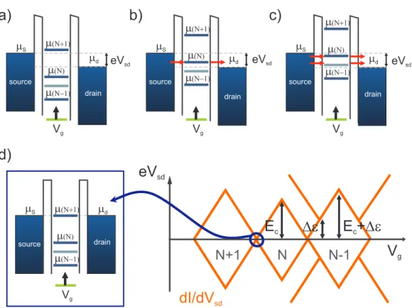
by varying the electrostatic potential of the dot with a gate voltage (see Figs.2.8 a)-c)). Each channel brought into the bias window results in a step in the measured current I, and therefore, a peak in differential conductance
dI/dVsd ≡ G, as illustrated in Fig.2.7 d).
Fig.2.8 d) shows the diamond-shaped diagram obtained when dI/dVsd
is monitored while sweeping Vsd and stepping Vg [2]. This is the stability
diagram of the device, where the area inside the diamonds corresponds to a Coulomb blockaded region in which the amount of charges on the dot
is fixed. In the constant interaction model [2], the height in eVsd of these
diamonds is defined as the addition energy (Eadd) and it consists of a purely
electrostatic part (Ec) plus the energy spacing between two discrete quantum
levels (∆ε). ∆ε can be zero if consecutive carriers are added to the same spin-degenerate level. This is the reason why the stability diagram of QDs with well-separated spin-degenerate levels consists of a regular sequence of large and small Coulomb diamonds corresponding to even and odd filling, respectively.
The inset of Fig.2.8 d) exhibits the case in which, by moving the elec-trochemical potential ladder, a transport channel can be activated even at a very small bias. This occurs at the so-called degenerate points, found at the crossing of two diamond regions.
Until now, we have treated the tunneling to lowest order in perturbation theory, i.e. just direct tunneling processes were described. However, in the regime of Coulomb blockade, higher-order processes may become important
when the resistances of the tunnel junctions begin to approach e2/h, where
GS ES
V
sdI
a)
eVsd mS md source drain eVsd mS md source drain eVsd mS md source drainV
b)
c)
dI/dV
sdd)
m(N+1) m(N-1) m(N) m(N+1) m(N-1) m(N) m(N+1) m(N-1) m(N)Figure 2.7: Schematic diagrams of the electrochemical potential levels for different bias voltages. The level in gray corresponds to a channel involving an excited state for N − 1 carriers. a) No electrochemical potential level of
the dot falls within the bias window (eVsd) set by µs and µd. The charge
number in the island is then fixed at N . b) µ(N ) is in the bias window, transport can take place through this channel and as a consequence, the amount of charge carriers in the dot alternates between N and N − 1. c) The bias window is big enough to allow transport through two channels; one of them involves ground states and the other, a ground state and an excited state. d) Current flow through the device (I) and differential conductance
(dI/dVsd) for each case represented in a), b) and c). A channel which is open
for transport appears as a step in the measured current and as a peak in differential conductance.
eV
sda)
eVsd mS md source drain mS md source drain mS md source drainb)
c)
dI/dV
sd eVsd eVsd Vg Vg VgN+1
N
N-1
V
gE
cDe
d)
mS md source drain m(N+1) m(N-1) m(N) m(N+1) m(N-1) m(N) m(N+1) m(N-1) m(N) Vg m(N+1) m(N-1) m(N)E +
cDe
Figure 2.8: Schematic diagrams of the electrochemical potential levels for
different gate voltages (Vg). The level in gray represents a transition to an
excited state for N − 1 carriers. The cases a), b) and c) are analogous to the ones on Fig.2.7 with the difference that the bias window is kept fixed and the electrochemical potential ladder is moved by a positive voltage applied to the gate. d) Diamond-shaped stability diagram. The differential conductance is
displayed as a function of Vg and Vsd. The charging energy Ec plus the energy
spacing between levels ∆ε is needed to activate the transport through the dot. ∆ε can be zero when a second carrier is added to a spin-degenerate level. This case is illustrated by the diamond corresponding to N charges. The diamond region for N − 1 exhibits lines representing transport through the excited state. It is important to remark that in most of the experiments discussed in this thesis, the charge carriers are holes and consequently, a positive variation of a gate voltage will lead to the depletion of the QD. Inset: Zero-bias transport takes place at the degenerate points, where an electrochemical potential level aligns with the electrochemical potential of the leads.
2.3.2
Elastic and inelastic cotunneling processes
In a first order process, a particle cannot tunnel from the leads to the dot when biased in the Coulomb blockade regime due to conservation of energy. However, higher order processes allow the transfer of a charge carrier from the left lead to the right lead (or vice versa) via a virtual state in the island. These processes may be either elastic or inelastic. Elastic cotunneling is the dominant off-resonance process at low bias. It gives rise to current inside the Coulomb diamond (light grey region in Fig.2.9 a)). The corresponding two-electron process (Fig.2.9 b)) transfers one carrier from the left to the right lead, thereby leaving the dot in the ground state.
Similar two-electron processes can occur which drive the dot into an ex-cited state. For instance, a carrier can leave the dot from the ground state to the lowest Fermi sea, while another carrier from the highest Fermi sea tunnels into the excited state (see Fig.2.9 c)). Although this type of process is called inelastic [28], the total electron energy is conserved. The on-site excitation
is created at the expense of the energy drop eVsd. To first approximation,
the onset of inelastic cotunneling yields a step in dI/dVsd [29], as depicted in
Fig.2.9 a).
2.4
First hybrid devices on SiGe self-assembled
quantum dots
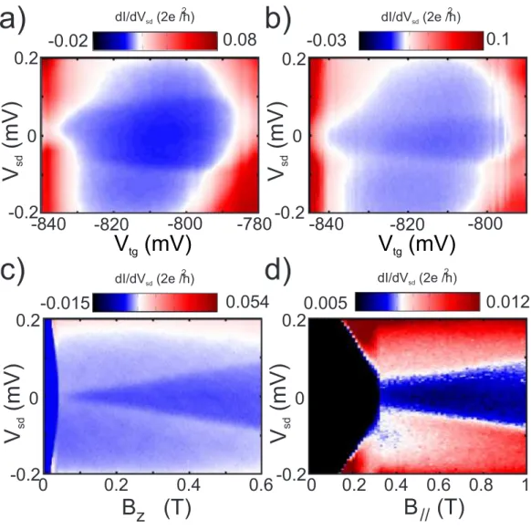
A big advantage of self-assembled semiconductor QD is that metal leads can be deposited directly on top of the nanostructure, allowing thus to explore different types of metals as contacts. A variety of hybrid devices can be envisioned, which combine metal properties, as superconductivity or ferro-magnetism, with the microscopic properties of the QD.
The first low-temperature transport measurements on SiGe self-assembled QDs were performed and published by the group [13]. The scheme of the device is the one shown in Fig.2.3 a). Single-hole tunneling was observed and discrete energy spectra with ∆ε up to a few meV were reported (see Fig.2.10). The measurements were taken at a base temperature of 15 mK and the islands were contacted by Al leads, though devices with Ti/Au and Pt contacts have also been tested. Very low contact resistances were found in the latter case.
So far it has not been possible to deplete the SiGe islands. The reason for this is that the gate voltage also influences the capacitance between the dot and its leads, leading to different coupling regimes. When a large positive gate voltage is applied in order to deplete the QD, the coupling to the leads
m
Sm
d source draineV
sddI/dV
sdV
ge|V |=
sdD
Em
Sm
d source drain DED
Ea)
b)
c)
DED
EFigure 2.9: a) Illustration of a Coulomb diamond. In the light-blue area, conduction is due to elastic cotunneling via virtual events as shown in b).
For eVsd ≥ ∆E, inelastic processes, illustrated in c), increase the cotunneling
current (dark-blue areas). ∆E is the energy spacing between the ground state
and the first excited state, which in b) and c) are represented by blue and grey lines, respectively.
becomes very weak. As a consequence, it is not possible to conclude whether the unmeasurable current results from the depletion of the QD or from a very low tunneling rate. The effect of the gate voltage on the capacitance between the nanostructure and the metal contacts can be observed in Fig.2.10, where an increasing size of the diamonds towards positive voltages evidences mainly
an increasing Ec and thus, a decreasing Ceq.
The last three diamonds in Fig.2.10 show size alternation, implying that
the Nth carrier is a s = 1
2 particle added to a spin-degenerate level, as a
smaller Eadd is observed in this case. Noteworthy, spectroscopy on dots
containing more than two charge carriers has shown important deviations from an alternating spin filling scheme [30, 31].
For these SiGe self-assembled islands, strong spin-orbit coupling and res-onant supercurrent transport have been reported in [13] among other spin-related phenomena.
2.5
Hole g-factor measurements in SiGe
self-assembled nanostructures
When an external magnetic field ~B is applied, additional lines in dI/dVsd
appear around those diamonds that correspond to an odd number of confined charges. These additional lines result from the splitting of the energy levels
caused by the lifting of the spin degeneracy in the presence of a ~B. The
energy difference between the split levels, the so-called Zeeman energy, is given by
∆Ez = kgµBBk,~ (2.1)
where µB is Bohr’s magneton and g is the g-factor tensor. This tensor
is related to the electronic structure of the system. Therefore, the g-factor depends on many factors, among which we find the spin-orbit coupling [32] and the confinement potential [33, 34].
In absence of magnetic field, the ground state of a dot with an even occupation has an integer spin, S. In the case of well separated levels, the
ground state is a spin singlet (S = 0), |Si = (|↑↓i − |↓↑i)/√2 [35]. In this
case, the highest occupied orbital is filled with two electrons with opposite spins.
The first excited states are the spin triplets (S = 1), where one charge is promoted to the first available empty orbital. The three triplet states are degenerate at zero magnetic field, but the Zeeman energy shift under finite
N+1
N
N-1
De
3 4 5 6
20
10
0
-10
-20
I (nA)
V
(mV)
sdV (V)
bg-10
10
Figure 2.10: Stability diagram of a SiGe island coupled to Al leads taken from [13]. A 50 mT magnetic field perpendicular to the substrate plane was applied in order to suppress the superconductivity in the contacts. The
current through the device is measured while sweeping Vsd and stepping the
back-gate voltage, Vbg. A discrete energy spectrum is evidenced by steps
in the current corresponding to the opening of transport channels involving excited states. The energy spacing ∆ε is indicated for one of these transitions. It is important to remark that, as the charge carriers are holes, the number
for |T+i = | ↑↑i, Sz = 0 for |T0i = (| ↑↓i + | ↓↑i)/
√
2 and Sz = −1 for
|T−i = | ↓↓i.
The split energy levels, the ladder in electrochemical potentials for the allowed transitions and the corresponding lines in the stability diagram for
a finite ~B, are illustrated in Fig.2.11 a) [2]. Fig.2.11 b) exhibits a
differen-tial conductance measurement performed on a SiGe island contacted with Al leads in the presence of an external magnetic field perpendicular to the
substrate plane Bz. The magnetic field causes a splitting of the diamond
edges as indicated by green rhombi. This splitting follows from the lifting of the degeneracy in the ground states associated with the side diamonds. We thus conclude that the central diamond corresponds to an even number N
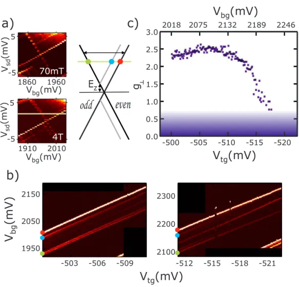
of confined holes [2]. g⊥ = (3.0 ± 0.4) and g⊥ = (2.8 ± 0.4) are extracted for
the right and the left diamond ground states, respectively 2. The error bar
on these measurements is given by the uncertainty in energy introduced by the life-time broadening of the confined energy states.
The line indicated by a star in Fig.2.11 b) is due to the spin-triplet excited state for N holes on the QD. We measure a 2 meV singlet-triplet energy in this particular device, which is an order of magnitude larger than for electrons in Si/SiGe heterostructures [36]. Noteworthy, large singlet-triplet excitation energies are particularly desirable for the observation of spin blockade in
double-dot experiments [37]. Upon increasing Bz, the line denoted by a star
splits as shown by the emergence of a second parallel line, indicated by a
circle, that shifts away proportionally to Bz (see Figs.2.11 b) CENTER and
RIGHT). This behaviour corresponds to the Zeeman splitting of the excited
spin-triplet state [2] with g⊥ = (2.8 ± 0.4).
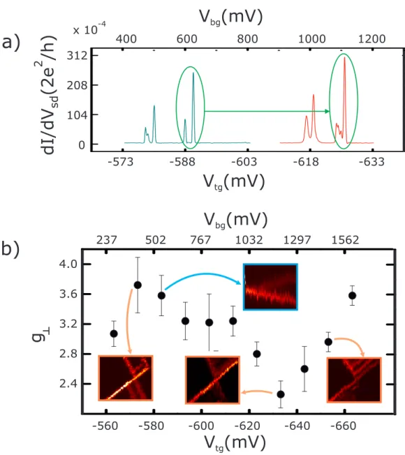
The Zeemann energy can also be extracted from cotunneling spectroscopy, as shown in Fig.2.12. Due to the fact that the smearing of the cotunneling step is uniquely determined by the electronic temperature [38], at very low temperatures the cotunneling spectroscopy provides a high resolution tool to estimate the Zeeman energy.
As mentioned before, the g tensor is affected by multiple electronic prop-erties, and thus the measured g-factors differ substantially from the free-electron value (2.002). g also exhibits a pronounced anisotropy; in Fig.2.13 a) the Zeeman energy is measured in inelastic cotunneling as a function of
Bz and Bk [13]. g⊥ ≈ 2.7 and gk ≈ 1.2 are the extracted g-factor
val-ues in the perpendicular and parallel plane, respectively. This anisotropy is qualitatively consistent with calculations for pure Ge islands [39].
Simi-2
Since we measure ∆Ez and we extract g from Eq.2.1, we have no information about
the sign of g. Therefore, throughout this thesis, measured values of g will always stand for the absolute value of this magnitude. As will be discussed in Chapter 3, the sign of g⊥
odd
even
70mT 4T DEz N (odd) N+1 (even) S T+ T0 T -DEz DEz DEz -540 -525 V (mV)g V (mV) sd 4 3 2 1 0 -1 -2 -3 -4 0.5 1 1.5 2 2.5 3x 10⁻³ 4 3 2 1 0 -1 -2 -3 -4 V (mV) sd 4 3 2 1 0 -1 -2 -3 -4 V (mV) sd -540 -525 V (mV)g -540 -525 V (mV)g odda)
b)
Em
DEz DEz EST EST Vg Vsd 4T 4T dI/dV (2e /h)sd 2 N (even) N+1 N-1 odd N (even) N+1 N-1 N (even) N+1 N-1 B = 70 mTz B = 3 Tz B = 5 TzFigure 2.11: a) LEFT: Schematic energy diagram showing the split energy
levels for an even and odd occupation of the island, being ∆Ez the
Zee-man energy and EST the singlet-triplet energy difference at B = 0. The
coloured vertical arrows represent excitations allowed by the spin selection
rule (|∆Sz| = 1/2). We note that ↑↔ T− and ↓↔ T+ are not allowed.
CEN-TER: Electrochemical potential ladder for the transitions on the right using the same color coding. RIGHT: Schematics of a stability diagram plot where the lines corresponding to the allowed transition are illustrated. The color
coding is also respected. b) dI/dVsd as a function of Vsd and Vg for a SiGe
device contacted by Al leads and measured at a base temperature of ∼ 250
mK. LEFT: Bz = 70 mT, the line corresponding to the singlet-triplet
tran-sition is indicated. The purpose of this small magnetic field is to suppress
the superconductivity of the Al contacts. CENTER, RIGHT: Bz = 3 T,
Bz = 5 T respectively. The transitions in a) are indicated with symbols of
corresponding colors. The lines indicated by green rhombi correspond to the onset of tunneling via Zeeman-split levels for N − 1 and N + 1 holes on the QD. The lines indicated by a star and a circle correspond to singlet-triplet excitations for N holes. Noteworthy, some of these transitions are visible for negative bias voltages, while they are not for positive values of the latter.
eVsd mS md source drain eVsd mS md source drain DEz 4.5 4.55 2 1 0 -1 -2 V (mV) sd V (V)g dI/dVsd DEz odd even eV = Esd D z S S S S S
Figure 2.12: CENTER: dI/dVsd as a function of Vsd and Vg is shown for
a SiGe device in the presence of Bz = 8 T at 15 mK. Taken from [13].
RIGHT: Scheme of the direct tunneling process that gives rise to the line indicated in the center plot. LEFT: Inelastic cotunneling leading to the step
in dI/dVsd indicated in the center plot. This process activates when the bias
voltage equals the difference in energy between the two electrochemical levels, i.e. when the bias coincides with the Zeeman energy. Inelastic cotunneling spectroscopy provides thus an additional way to measure the g-factor. From
the observed step in dI/dVsd, g⊥ ≈ 3 was extracted.
lar anisotropies have also been reported for strained bulk Ge [40], acceptor levels in Si/Ge/Si heterostructures [41] and Ge/Si core-shell nanowires [42]. A characterization of the Zeeman energy as a function of the magnetic field angle is shown in Fig.2.13 b).
In [13] it has also been shown that g depends on the number of confined holes, i.e. on the diamond chosen for the Zeeman energy estimation (see Fig.2.13 c)).
a)
V
(mV)
sddI/dV (2e /h)
sd 2V (V)
gc)
b)
V
(mV)
sdd I/d V
2 2 sd Bz B//Figure 2.13: a) dI/dVsd as a function of Bz and Bk. To a good approximation,
the Zeeman energy, given by the dI/dVsd position of the inelastic-cotunneling
steps, increases linearly with magnetic field, in agreement with Eq. 2.1. The features around B = 0 arise from the superconductivity of the aluminium
contacts. b) Numerical derivative of dI/dVsd as a function of the magnetic
field angle with respect to the substrate plane. The minimum Zeeman energy, which does not correspond to a parallel B, is indicated by a white arrow. At
this angle, gmin ∼ 0.5 is estimated. c) Absolute values of g⊥and gk measured
for the same device at different number of confined charges. a), b) and c) were taken from [13].
Chapter 3
Electrically tunable g-factor
By means of electron spin resonance (ESR) techniques, coherent spin rota-tions can be induced. Usually, for an ESR to occur, the confined spin is exposed to an alternating magnetic field [43, 44, 45, 46]. However, because strong local oscillatory electric fields are easier to obtain than strong local oscillatory magnetic fields, interest has focused in spin resonance induced by electric fields. As mentioned in Chapter 1, spin-orbit coupling has been used to achieve an electric-dipole induced spin resonance (EDSR) in QDs [22, 23, 21]. For this technique, an external electric field is applied to the QD via a gate electrode to which an ac signal is supplied from an external circuit. An external static magnetic field induces the Zeeman splitting and secures the spin-electric coupling via the spin-orbit interaction [21]. As shown in [47], spin manipulation can also be achieved through fast control of the exchange coupling.
Another possibility for electric-field spin manipulation is the g-tensor modulation resonance, which has been used on ensembles of spins in two-dimensional electron systems [48, 49]. This technique relies on anisotropic and electrically tunable g-factors.
Recently, several experiments have addressed the g-factor modulation by means of external electric fields [50, 51], and different mechanisms were evoked to explain the observed g-factor tunability, such as compositional gradients [50] and quenching of the angular momentum [51, 52].
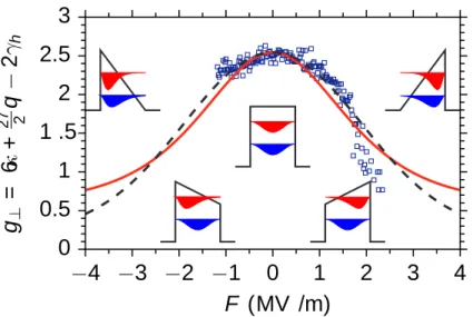
In this chapter, the experimental observation of an exceptionally large and non-monotonic electric-field modulation of the hole g-factor in SiGe QDs is discussed. To interpret this finding we invoke a new mechanism that applies to hole-type low-dimensional systems. This mechanism relies on the existence of an important, yet overlooked correction term in the g-factor whose magnitude depends on the mixing of heavy and light holes. The work presented in this chapter has lead to two publications [53, 54].


![Figure 2.10: Stability diagram of a SiGe island coupled to Al leads taken from [13]. A 50 mT magnetic field perpendicular to the substrate plane was applied in order to suppress the superconductivity in the contacts](https://thumb-eu.123doks.com/thumbv2/123doknet/12872218.369364/42.892.153.731.262.767/figure-stability-magnetic-perpendicular-substrate-suppress-superconductivity-contacts.webp)