Visualizing Plasmonic Coupling in Metamaterials and Applying Angular Resolved
EELS
Felix von Cube1,2,3, Jens Niegemann4, David C. Bell1 , Stephan Irsen3 and Stefan Linden2
1. School of Engineering and Applied Sciences, Harvard University, Cambridge, MA, USA.
2. Physikalisches Institut, Universität Bonn, Bonn, Germany.
3. Electron Microscopy and Analysis (EMA), Center of Advanced European Studies and Research
(caesar), Bonn, Germany.
4. Laboratory for Electromagnetic Fields and Microwave Electronics, Swiss Federal Institute of
Technology (ETH), Zürich, Switzerland.
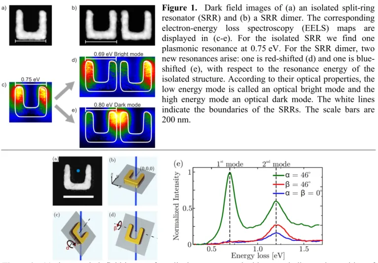
The metamaterial concept has introduced numerous fascinating phenomena to optics and photonics, as for example a negative index of refraction. In most cases, the origin of such a phenomenon can be traced back to the excitation of plasmonic resonances in the building blocks of the metamaterial. Hence, the knowledge of the plasmonic near-fields is of upmost interest for an in-depth understanding of the properties of a given metamaterial. One of the paradigm metamaterial is the split-ring resonators (SRR), it is a subwavelength metallic ring with a slit (Fig. 1a). We perform electron energy-loss spectroscopy (EELS) on lithographically defined gold SRRs to map the electric near-field distribution of their plasmonic resonances. We use EELS in combination with scanning transmission electron microscopy (STEM) allowing for nanometer spatial and sub eV energetic resolution [1]. For a given electron loss energy, strong EELS signals are expected, if the excited plasmonic resonance has a large electric field component Ez along the trajectory (z-axis) of the electron beam. In case of an isolated SRR, the first
plasmonic resonance shows two strong electric field components at the arms of the structure (Fig. 1c). Metamaterials usually consist not only of one isolated structure, but of thousands of structures, therefore we are interested in the coupling behavior of two or more SRRs. In case of a SRR dimer, the electromagnetic coupling leads to the formation of two new plasmonic resonances, one slightly red shifted and one slightly blue shifted (Fig. 1 d,e). The formation of these new resonances can be explained with a classical dipole model, in which the dipoles oscillate either in-phase or out-of-phase. Furthermore, we observe that coupling in small SRR ensembles results in the formation of discrete eigenmodes where the number of modes corresponds to the number of SRRs. However, the EELS maps of large arrays, containing thousands of SRRs, show the formation of a quasi-continuum of modes, which is in accordance with the plasmon hybridization model [2, 3].
We also investigate the plasmonic near-field with angular resolved EELS. By tilting the sample, different electric field components of the plasmonic modes can be probed with the electron beam. This allows us to detect the Ex and Ey components of the electric near-field, in addition to the Ez component,
which is probed in conventional EELS. The electron energy-loss spectra recorded under oblique incidence feature plasmonic resonances that are not observable under normal incidence (Fig. 2). Our experimental findings are reproduced by full numerical calculations based on the discontinuous Galerkin time-domain method [4].
In conclusion, we have used STEM-EELS to investigate the electric near-field of plasmon resonances on SRRs. We observe coupling effects in ensembles of two and more SRRs which result in the formation of
Paper No. 1191 2385
doi:10.1017/S1431927615012702 © Microscopy Society of America 2015
Microsc. Microanal. 21 (Suppl 3), 2015
https://doi.org/10.1017/S1431927615012702
new plasmonic modes. Additionally we have performed angular resolved EELS to get a three dimensional insight on the electric near-field [5].
References:
[1] J. Nelayah et al, Nat. Phys. 3 (2007), p. 348. [2] F. von Cube et al, Nano Letters 13 (2013), p. 703. [3] P. Nordlander et al, Nano Letters 4 (2004), p. 899.
[4] F. von Cube et al, Physical Review B 89 (2014), p. 115434.
[5] S.I. and S.L. acknowledge the financial support of the DFG-Project LI 1641/2-1. F.v.C. acknowledges financial support by the DAAD.
This work was performed in part at the Center for Nanoscale Systems (CNS), a member of the National Nanotechnology Infrastructure Network (NNIN), which is supported by the National Science
Foundation under NSF award no. ECS-0335765. CNS is part of Harvard University.
Figure 1. Dark field images of (a) an isolated split-ring
resonator (SRR) and (b) a SRR dimer. The corresponding electron-energy loss spectroscopy (EELS) maps are displayed in (c-e). For the isolated SRR we find one plasmonic resonance at 0.75 eV. For the SRR dimer, two new resonances arise: one is red-shifted (d) and one is blue-shifted (e), with respect to the resonance energy of the isolated structure. According to their optical properties, the low energy mode is called an optical bright mode and the high energy mode an optical dark mode. The white lines indicate the boundaries of the SRRs. The scale bars are 200 nm.
Figure 2. (a) shows a dark-field image of a split ring resonator, the blue spot indicates the position of
the fixed electron beam; the scale bar is 200 nm. (b-d) scheme the different sample orientations: (b) conventional (orthogonal) electron incidence, (c) sample tilt around the y-axis, and (d) sample tilt around the x-axis. (e) EEL spectra recorded at the position shown in (a) for different tilt-angles. The vertical dashed lines indicate the resonance-energies of the first-order and second-order plasmonic mode. For a tilt around the y-axis we find a strong resonance, which cannot be found under orthogonal electron beam incidence.
2386 Microsc. Microanal. 21 (Suppl 3), 2015
https://doi.org/10.1017/S1431927615012702