Publisher’s version / Version de l'éditeur:
Optics Express, 24, 12, pp. 12893-12904, 2016
READ THESE TERMS AND CONDITIONS CAREFULLY BEFORE USING THIS WEBSITE. https://nrc-publications.canada.ca/eng/copyright
Vous avez des questions? Nous pouvons vous aider. Pour communiquer directement avec un auteur, consultez la première page de la revue dans laquelle son article a été publié afin de trouver ses coordonnées. Si vous n’arrivez Questions? Contact the NRC Publications Archive team at
PublicationsArchive-ArchivesPublications@nrc-cnrc.gc.ca. If you wish to email the authors directly, please see the first page of the publication for their contact information.
NRC Publications Archive
Archives des publications du CNRC
This publication could be one of several versions: author’s original, accepted manuscript or the publisher’s version. / La version de cette publication peut être l’une des suivantes : la version prépublication de l’auteur, la version acceptée du manuscrit ou la version de l’éditeur.
For the publisher’s version, please access the DOI link below./ Pour consulter la version de l’éditeur, utilisez le lien DOI ci-dessous.
https://doi.org/10.1364/OE.24.012893
Access and use of this website and the material on it are subject to the Terms and Conditions set forth at
Single-etch subwavelength engineered fiber-chip grating couplers for
13 µm datacom wavelength band
Benedikovic, Daniel; Alonso-Ramos, Carlos; Cheben, Pavel; Schmid, Jens
H.; Wang, Shurui; Halir, Robert; Ortega-Moñux, Alejandro; Xu, Dan-Xia;
Vivien, Laurent; Lapointe, Jean; Janz, Siegfried; Dado, Milan
https://publications-cnrc.canada.ca/fra/droits
L’accès à ce site Web et l’utilisation de son contenu sont assujettis aux conditions présentées dans le site LISEZ CES CONDITIONS ATTENTIVEMENT AVANT D’UTILISER CE SITE WEB.
NRC Publications Record / Notice d'Archives des publications de CNRC:
https://nrc-publications.canada.ca/eng/view/object/?id=c68c8a52-834f-4063-964a-ff96aeb5e037 https://publications-cnrc.canada.ca/fra/voir/objet/?id=c68c8a52-834f-4063-964a-ff96aeb5e037Single-etch subwavelength engineered fiber-chip
grating couplers for 1.3 µm datacom wavelength
band
Daniel Benedikovic,1,* Carlos Alonso-Ramos,1,5 Pavel Cheben,2,6 Jens H. Schmid,2 Shurui Wang,2 Robert Halir,3 Alejandro Ortega-Moñux,3 Dan-Xia Xu,2 Laurent
Vivien,1 Jean Lapointe,2 Siegfried Janz,2 and Milan Dado4 1
Institut d’Electronique Fondamentale, Université Paris Sud, CNRS, UMR8622, Université Paris-Saclay, Bat. 220, Orsay Cedex, France
2National Research Council Canada, Information and Communication Technologies, 1200 Montreal Road, Ottawa,
Ontario K1A0R6, Canada
3Dpto. de Ingeniería Comunicaciones, ETSI Telecomunicación, Universidad de Málaga, 29010 Málaga, Spain 4University of Žilina, Faculty of Electrical Engineering, Department of Telecommunications and Multimedia,
Univerzitná 8215/1, 010 26 Žilina, Slovakia
5carlos.ramos@u-psud.fr 6pavel.cheben@nrc.ca
*daniel.benedikovic@u-psud.fr
Abstract: We report, for the first time, on the design and experimental demonstration of fiber-chip surface grating couplers based on subwavelength grating engineered nanostructure operating in the low fiber chromatic dispersion window (around 1.3 μm wavelengths), which is of great interest for short-reach data communication applications. Our coupler designs meet the minimum feature size requirements of large-volume deep-ultraviolet stepper lithography processes. The fiber-chip couplers are implemented in a standard 220-nm-thick silicon-on-insulator (SOI) platform and are fabricated by using a single etch process. Several types of couplers are presented, specifically the uniform, the apodized, and the focusing designs. The measured peak coupling efficiency is −2.5 dB (56%) near the central wavelength of 1.3 μm. In addition, by utilizing the technique of the backside substrate metallization underneath the grating couplers, the coupling efficiency of up to −0.5 dB (89%) is predicted by Finite Difference Time Domain (FDTD) calculations.
©2016 Optical Society of America
OCIS codes: (130.0130) Integrated optics; (050.1950) Diffraction gratings; (250.5300) Photonic integrated circuits; (050.6624) Subwavelength structures; (160.3918) Metamaterials.
References and links
1. A. Rickman, “The commercialization of silicon photonics,” Nat. Photonics 8(8), 579–582 (2014).
2. T.-Y. Liow, J. Song, X. Tu, A. E.-J. Lim, Q. Fang, N. Duan, M. Yu, and G.-Q. Lo, “Silicon optical interconnect device technologies for 40 Gb/s and beyond,” IEEE J. Sel. Top. Quantum Electron. 19(2), 8200312 (2013). 3. A. Mekis, S. Gloeckner, G. Masini, A. Narasimha, T. Pinguet, S. Sahni, and P. De Dobbelaere, “A
grating-coupler-enabled CMOS photonics platform,” IEEE J. Sel. Top. Quantum Electron. 17(3), 597–608 (2011). 4. S. Romero-García, B. Shen, F. Merget, B. Marzban, and J. Witzens, “Alignment tolerant couplers for silicon
photonics,” IEEE J. Sel. Top. Quantum Electron. 21(6), 8200214 (2015).
5. P. Cheben, J. H. Schmid, S. Wang, D.-X. Xu, M. Vachon, S. Janz, J. Lapointe, Y. Painchaud, and M.-J. Picard, “Broadband polarization independent nanophotonic coupler for silicon waveguides with ultra-high efficiency,” Opt. Express 23(17), 22553–22563 (2015).
6. Ch. Kopp, S. Bernabé, B. B. Bakir, J.-M. Fédéli, R. Orobtchouk, F. Schrank, H. Porte, L. Zimmermann, and T. Tekin, “Silicon photonic circuits: on-CMOS integration, fiber optical coupling, and packaging,” IEEE J. Sel. Top. Quantum Electron. 17(3), 498–509 (2011).
7. D. Taillaert, P. Bienstman, and R. Baets, “Compact efficient broadband grating coupler for silicon-on-insulator waveguides,” Opt. Lett. 29(23), 2749–2751 (2004).
8. X. Chen, Ch. Li, Ch. K. Y. Fung, S. M. G. Lo, and H. K. Tsang, “Apodized Waveguide Grating Couplers for Efficient Coupling to Optical Fibers,” IEEE Photonics Technol. Lett. 22(15), 1156–1158 (2010).
9. C. Zhang, J.-H. Sun, X. Xiao, W.-M. Sun, X.-J. Zhang, T. Chu, J.-Z. Yu, and Y.-D. Yu, “High efficiency grating coupler for coupling between single-mode fiber and SOI waveguides,” Chin. Phys. Lett. 30(1), 014207 (2013). 10. D.-X. Xu, J. H. Schmid, G. T. Reed, G. Z. Mashanovich, D. J. Thomson, M. Nedeljkovic, X. Chen, D. Van
Thourhout, S. Keyvaninia, and S. K. Selvaraja, “Silicon photonic iIntegration platform - Have we found the sweet spot?” IEEE J. Sel. Top. Quantum Electron. 20(4), 189–205 (2014).
11. C. Li, H. Zhang, M. Yu, and G. Q. Lo, “CMOS-compatible high efficiency double-etched apodized waveguide grating coupler,” Opt. Express 21(7), 7868–7874 (2013).
12. A. Bozzola, L. Carroll, D. Gerace, I. Cristiani, and L. C. Andreani, “Optimising apodized grating couplers in a pure SOI platform to -0.5 dB coupling efficiency,” Opt. Express 23(12), 16289–16304 (2015).
13. A. E.-J. Lim, J. Song, Q. Fang, Ch. Li, X. Tu, N. Duan, K. K. Chen, R. P.-Ch. Tern, and T.-Y. Liow, “Review of silicon photonics foundry efforts,” IEEE J. Sel. Top. Quantum Electron. 20(4), 405–416 (2014).
14. W. S. Zaoui, A. Kunze, W. Vogel, M. Berroth, J. Butschke, F. Letzkus, and J. Burghartz, “Bridging the gap between optical fibers and silicon photonic integrated circuits,” Opt. Express 22(2), 1277–1286 (2014). 15. L. Carroll, D. Gerace, I. Cristiani, and L. C. Andreani, “Optimizing polarization-diversity couplers for
Si-photonics: reaching the -1dB coupling efficiency threshold,” Opt. Express 22(12), 14769–14781 (2014). 16. D. Benedikovic, P. Cheben, J. H. Schmid, D.-X. Xu, B. Lamontagne, S. Wang, J. Lapointe, R. Halir, A.
Ortega-Moñux, S. Janz, and M. Dado, “Subwavelength index engineered surface grating coupler with sub-decibel efficiency for 220-nm silicon-on-insulator waveguides,” Opt. Express 23(17), 22628–22635 (2015). 17. S. Romero-García, F. Merget, F. Zhong, H. Finkelstein, and J. Witzens, “Visible wavelength silicon nitride
focusing grating coupler with AlCu/TiN reflector,” Opt. Lett. 38(14), 2521–2523 (2013).
18. D. Benedikovic, P. Cheben, J. H. Schmid, D.-X. Xu, J. Lapointe, S. Wang, R. Halir, A. Ortega-Moñux, S. Janz, and M. Dado, “High-efficiency single etch step apodized surface grating coupler using subwavelength structure,” Laser Photonics Rev. 8(6), L93–L97 (2014).
19. Y. Ding, C. Peucheret, H. Ou, and K. Yvind, “Fully etched apodized grating coupler on the SOI platform with -0.58 dB coupling efficiency,” Opt. Lett. 39(18), 5348–5350 (2014).
20. C. Baudot, D. Dutartre, A. Souhaité, N. Vulliet, A. Jones, M. Ries, A. Mekis, L. Verslegers, P. Sun, Y. Chi, S. Cremer, O. Gourhant, D. Benoit, G. Courgoulet, C. Perrot, L. Broussous, T. Pinguet, J. Siniviant, and F. Boeuf, “Low Cost 300 mm double-SOI substrate for low insertion loss 1D & 2D grating couplers,” in Proceedings of
IEEE 11th International on Group IV Photonics (GFP) (IEEE, 2014), pp. 137–138.
21. D. Vermeulen, S. Selvaraja, P. Verheyen, G. Lepage, W. Bogaerts, P. Absil, D. Van Thourhout, and G. Roelkens, “High-efficiency fiber-to-chip grating couplers realized using an advanced CMOS-compatible silicon-on-insulator platform,” Opt. Express 18(17), 18278–18283 (2010).
22. C. Alonso-Ramos, A. Ortega-Moñux, L. Zavargo-Peche, R. Halir, J. de Oliva-Rubio, I. Molina-Fernández, P. Cheben, D.-X. Xu, S. Janz, N. Kim, and B. Lamontagne, “Single-etch grating coupler for micrometric silicon rib waveguides,” Opt. Lett. 36(14), 2647–2649 (2011).
23. C. Alonso-Ramos, P. Cheben, A. Ortega-Moñux, J. H. Schmid, D.-X. Xu, and I. Molina-Fernández, “Fiber-chip grating coupler based on interleaved trenches with directionality exceeding 95,” Opt. Lett. 39(18), 5351–5354 (2014).
24. M. Fan, M. A. Popović, and F. X. Kartner, “High directivity, vertical fiber-to-chip coupler with anisotropically radiating grating teeth,” in Conference on Lasers and Electro-Optics/Quantum Electronics and Laser Science
Conference and Photonic Applications Systems Technologies (Optical Society of America, 2007), paper
CTuDD3.
25. D. Benedikovic, C. Alonso-Ramos, P. Cheben, J. H. Schmid, S. Wang, D.-X. Xu, J. Lapointe, S. Janz, R. Halir, A. Ortega-Moñux, J. G. Wangüemert-Pérez, I. Molina-Fernández, J.-M. Fédéli, L. Vivien, and M. Dado, “High-directionality fiber-chip grating coupler with interleaved trenches and subwavelength index-matching structure,” Opt. Lett. 40(18), 4190–4193 (2015).
26. L. Vivien, D. Pascal, S. Lardenois, D. Marris-Morini, E. Cassan, F. Grillot, S. Laval, J.-M. Fédéli, and L. El Melhaoui, “Light injection in SOI microwaveguides using high-efficiency grating couplers,” J. Lightwave Technol. 24(10), 3810–3815 (2006).
27. N. Na, H. Frish, I.-W. Hsieh, O. Harel, R. George, A. Barkai, and H. Rong, “Efficient broadband silicon-on-insulator grating coupler with low backreflection,” Opt. Lett. 36(11), 2101–2103 (2011).
28. R. Shi, H. Guan, A. Novack, M. Streshinsky, A. E.-J. Lim, G.-Q. Lo, T. Beahr-Jones, and M. Hochberg, “High-efficiency grating couplers near 1310 nm fabricated by 248-nm DUV lithography,” IEEE Photonics Technol. Lett. 26(15), 1569–1572 (2014).
29. R. Halir, P. Cheben, S. Janz, D.-X. Xu, I. Molina-Fernández, and J. G. Wangüemert-Pérez, “Waveguide grating coupler with subwavelength microstructures,” Opt. Lett. 34(9), 1408–1410 (2009).
30. R. Halir, P. Cheben, J. H. Schmid, R. Ma, D. Bedard, S. Janz, D.-X. Xu, A. Densmore, J. Lapointe, and I. Molina-Fernández, “Continuously apodized fiber-to-chip surface grating coupler with refractive index engineered subwavelength structure,” Opt. Lett. 35(19), 3243–3245 (2010).
31. X. Chen and H. K. Tsang, “Nanoholes grating couplers for coupling between silicon-on-insulator waveguides and optical fibers,” IEEE Photonics J. 1(3), 184–190 (2009).
32. R. Halir, L. Zavargo-Peche, D.-X. Xu, P. Cheben, R. Ma, J. H. Schmid, S. Janz, A. Densmore, A. Ortega-Moñux, I. Molina-Fernández, M. Fournier, and J.-M. Fédéli, “Single etch grating couplers for mass fabrication with DUV lithography,” Opt. Quantum Electron. 44(12–13), 521–526 (2012).
33. L. Zavargo-Peche, A. Ortega-Moñux, J. G. Wangüemert-Pérez, and I. Molina-Fernández, “Fourier based combined techniques to design novel sub-wavelength optical integrated devices,” Prog. Electromagnetics Res. 123, 447–465 (2012).
34. Optiwave [Online]. Available: http://www.optiwave.com/
35. R. Halir, P. Bock, P. Cheben, A. Ortega-Moñux, C. Alonso-Ramos, J. H. Schmid, J. Lapointe, D.-X. Xu, J. G. Wangüemert-Pérez, I. Molina-Fernández, and S. Janz, “Waveguide sub-wavelength structures: a review of principles and applications,” Laser Photonics Rev. 9(1), 25–49 (2015).
36. X. Chen and H. K. Tsang, “Polarization-independent grating couplers for silicon-on-insulator nanophotonic waveguides,” Opt. Lett. 36(6), 796–798 (2011).
37. X. Chen, K. Xu, Z. Cheng, C. K. Fung, and H. K. Tsang, “Wideband subwavelength gratings for coupling between silicon-on-insulator waveguides and optical fibers,” Opt. Lett. 37(17), 3483–3485 (2012). 38. S. M. Rytov, “Electromagnetic properties of a finely stratified medium,” Sov. Phys. 2, 466–475 (1956). 39. R. Waldhäusl, B. Schnabel, P. Dannberg, E.-B. Kley, A. Bräuer, and W. Karthe, “Efficient coupling into
polymer waveguides by gratings,” Appl. Opt. 36(36), 9383–9390 (1997).
40. F. Van Laere, T. Claes, J. Schrauwen, S. Scheerlinck, W. Bogaerts, D. Taillaert, L. O’Faolain, D. Van Thourhout, and R. Baets “Compact focusing grating couplers for silicon-on-insulator integrated circuits,” IEEE Photonics Technol. Lett. 19(23), 1919–1921 (2007).
41. Y. Li, L. Li, B. Tian, G. Roelkens, and R. G. Baets, “Reflectionless tilted grating couplers with improved coupling efficiency based on a silicon overlay,” IEEE Photonics Technol. Lett. 25(13), 1195–1198 (2013).
1. Introduction
Silicon-on-insulator (SOI) is a compelling photonic platform for implementation of complex photonic functions and waveguide circuits on a compact optoelectronic chip [1,2]. Optical input and output couplers are essential building blocks in the library of silicon photonic components [3–29]. Surface grating couplers are particularly interesting as they allow wafer-scale optical testing and yield comparatively large alignment tolerances for fiber attachment.
Recently, a number of different implemenations of surface grating couplers have been reported with a steady progress in increasing the fiber-chip coupling efficiency, particularly by optimizing the grating directionality and the field matching with the optical fiber mode. The field matching can be improved by using non-uniform (apodized) gratings with a variable coupling strength. This way, the exponential profile of the grating field is modified to match the near-Gaussian optical fiber mode profile [7]. However, this often requires small feature sizes of <100 nm [6,8,9], incompatible with 193 nm deep-ultraviolet (DUV) lithography. The grating directionality is another key factor for achieving high-efficiency designs [10]. Here, the goal is to increase the power coupled towards the superstrate, where the optical fiber is situated, and minimize the power radiated into the silicon substrate. Using Si waveguide layers thicker than 220 nm generally results in a substantially increased grating directionality [3,8,11,12]. However, the SOI with 220-nm-thick silicon presently dominates in multi project wafer (MPW) shuttles, offered by the publicly accessible silicon photonic foundries [10,13]. To date, the state-of-the-art solutions to maximize the grating directionality exploit comparatively complex structures [14–25], including backside wafer processing and metal mirror deposition [14–17], or bonding dielectric mirrors [3,6,7,18–20]. Yet another approach exploits the optimization of grating intrinsic directionality. This can be achieved for various asymmetric radiation geometries [21–25], specifically gratings with high-index overlays [21], judicious optimization of etch depths [11,22], or by the blazing effect [23–25].
Propagation loss in the optical fiber is a key parameter determining the performance and reach of long-haul photonic links. Conversely, short-reach datacom interconnects exhibit substantially relaxed loss requirements. Hence, they can migrate from the telecommunications C-band (around 1.55 µm wavelengths), where the optical fiber exhibits very low loss, to the O-band (around 1.3 µm wavelengths) to beneficially exploit the zero-dispersion feature of standard single-mode optical fibers. This wavelength band is of special interest for high-bandwidth applications in short-reach data communications such as Ethernet, cloud computing, or data storage, to name a few. However, silicon photonic components such as
surface grating couplers, were developed for operation in the C-band (near 1.55 µm) [1–25], with only a few notable exceptions reported for the O-band window (wavelength region near 1.3 µm) [26–28]. Specifically, Vivien et al. reported a 1.3 µm coupler in a custom-designed Unibond SOI wafer, with optimized silicon and BOX layer thicknesses [26]. Na et al. have demonstrated a uniform (unapodized) coupler in an SOI with a thicker (400 nm) Si layer for a hybrid laser design. The coupler was fabricated by a two-etch step process, yielding a coupling efficiency of −3 dB (50%) [27]. Shi et al. have demonstrated an apodized coupler in a 220-nm SOI, with an efficiency of −2 dB (63%) [28], but it also requires multiple etch steps.
While single-etch step subwavelength gratings have proven to be a cost-effective solution for the implementation of high-efficiency couplers in the C-band [16,29–32], no experimental or theoretical result has been reported on the use of subwavelength index engineered single-etch step grating couplers in the O-band. The main technical hurdle is the reduction in feature size required if a scaling approach is used to implement non-diffractive subwavelength grating nanostructures operating at 1.3 µm.
In this paper, we propose a comprehensive and general design procedure that enables the implementation of optimized subwavelength index engineered grating couplers with minimum feature sizes larger than 100 nm, compatible with large-volume fabrication processes like deep-ultraviolet stepper lithography. We also report, for the first time, on the design and experimental demonstration of 1.3 µm fiber-chip grating couplers with a subwavelength grating (SWG) engineered medium. The coupler is advantageously implemented in a standard 220 nm SOI photonic platform and fabricated using a single-etch step process.
2. Surface grating coupler design
The surface grating couplers are designed for an SOI wafer with a 220-nm-thick silicon waveguide layer and a 2-µm-thick SiO2 burried oxide (BOX). Air is assumed as the
superstrate medium. Silicon and silicon dioxide refractive indexes of nSi = 3.5047 and nSiO2 =
1.4484 at the wavelength of 1300 nm are used in the calculations. The design methodology is based on de-coupled two-dimensional (2-D) models in the vertical (y-z) and the horizontal (x-z) planes [29]. For simulations, Fourier-Eigenmode Expansion Method (F-EEM) [33] and Finite Difference Time Domain (FDTD) calculations [34] are used. Coupler schematics is shown in Fig. 1 ((a), vertical cross-section; (b), in-plane view).
Fig. 1. Schematics of an SWG index engineered surface grating coupler. (a) Vertical cross-section and (b) in-plane view. (c) Calculated SWG effective material index as a function of air gap widths for different SWG periods.
Grating couplers are designed for a single etch fabrication process. Both the grating region and the interconnecting waveguides are defined in the same step of lithography patterning and
etching, eliminating a second paterning step. This advantageous feature is afforded by utilization of the concept of subwavelength grating (SWG) refractive index engineering. The SWGs have successfully been used to locally engineer waveguide properties in integrated optical devices [16,18,19,25,29–31,35–37]. Here, we implement an SWG structure in the direction perpendicular to the light propagation, as a periodic arrangement of high-index material (silicon) segments and rectangular holes etched in the waveguide core. By controlling the SWG grating geometry, specifically the widths of the silicon segments (WSi,i)
and the air holes (WG,i) within the SWG period (ΛSWG = WSi,i + WG,i), a broad range of
effective material refractive indexes can be achieved, providing the SWG period is sufficiently small to frustrate all but the zeroth diffraction order [35,38]. In this configuration, the SWG period must be shorther than the Bragg period [29,35], ΛSWG < ΛBragg = λ/neff, where λ is the free-space wavelength (here, λ = 1.3 µm) and neff is the maximum effective index of
the slab waveguide fundamental TE-polarized mode (here, neff = 2.98). The range of effective
material indexes which can be synthesized directly depends on the duty cycle (WSi/ΛSWG)
range determined by the minimum feature size which can be implemented with a given fabrication process. In Fig. 1(c), the SWG refractive index is shown as a function of air gap width for different SWG periods. The SWG refractive index (an equivalent homogeneous material index) is calculated using a 2-D multilayer slab model in the horizontal plane [29]. As can be observed in Fig. 1(c), a wide range of effective material indexes can be synthesized, assuming a minimum feature size >100 nm, compatible with 193 nm DUV stepper lithography.
2.1 Uniform grating couplers with high directionality
The grating directionality, throughout this work is defined as the ratio between the power diffracted in upwards direction and the sum of the powers diffracted in upwards and downwards directions (D = Pup / (Pup + Pdown)) [14,23,25]. Grating directionality is typically limited by the interference effect due to the reflection at the interface between the BOX layer and the silicon substrate. We have demonstrated that a modification of the coupling angle is an effective technique to achieve the constructive interference condition [16,18].
Fig. 2. (a) Calculated grating directionality as a function of BOX thickness for two specific coupling angles (10° and 33°). (b) The grating directionality as a function of wavelength for different coupling angles.
In Fig. 2(a), the grating directionality is shown as a function of BOX thickness for two different coupling angles, 10° and 33°. It is observed that the grating directionality can readily be optimized for different BOX thicknesses by modifying the coupling angle. According to these calculations, the grating directionality is substantially enhanced for a standard 2-μm BOX thickness, yielding the peak value of 78% for a coupling angle of 33°, compared to 45% directionality for a coupling angle of 10°. The improved coupling performance is also observed in Fig. 2(b), which shows the grating directionality as a function of wavelength for different coupling angles. The geometrical parameters of the uniform grating coupler are:
diffraction grating period Λz = 800 nm, unetched silicon segment length LSi = 200 nm, SWG
trench length LSWG = 600 nm, and number of periods NP = 30 (see Fig. 1(a) and (b)). The
effective medium refractive index nSWG = 2.40 yields an optimal grating strength, with the
field overlap of 78% between the diffracted field and the near-Gaussian mode of the optical fiber (the maximum theoretical overlap between the exponential radiated field profile and the Gaussian fiber mode is ~80% [7],). In the present work, an SMF-28 optical fiber is used, with the mode field diameter MFD = 9.2 μm, defined at 1/e2 intensity and a wavelength of 1.3 μm.
The effective medium index of 2.40 is synthesized for the SWG air gap width WG = 166 nm
and SWG pitch ΛSWG = 400 nm (see Fig. 1(c)). The coupling efficiency of −2.4 dB (58%) is
calculated, with back-reflections of 5%. As shown in Fig. 3, our F-EEM calculations are in excellent agreement with FDTD simulations.
Fig. 3. Calculated coupling efficiency as a function of wavelength for the uniform, the two-step apodized, and the continuously apodized grating couplers.
2.2 Coupler apodization
Grating couplers are apodized by using SWG refractive index engineering. The variable grating strength along the mode propagation direction (z axis in Fig. 1(a)) is achieved by synthesizing different effective medium indexes in the subsequent SWG trenches. The apodization increases the field overlap with the optical fiber mode and it also reduces the effective index mismatch at the transition between the silicon access waveguide and the grating region, hence reducing back-reflections. Here we report on two types of apodization scheme, namely a two-step apodization and a continuous apodization. In both cases, the coupling angle is maintained constant (33°) for all grating segments. This is achieved by chirping the grating period in the apodized region to satisfy the phase matching condition:
sinΘ = nB,j/n0 + mλ/n0Λz,j. Here, Θ is the coupling angle, nB,j is the effective index of the Bloch-Floquet mode in the j-th grating segment, n0 is the refractive index of the superstrate
Fig. 4. (a) Calculated coupling efficiency of the two-step apodized coupler, for different numbers of periods in the first coupler section with the SWG index of nSWG = 2.85 and different SWG indexes in the second grating section of 24 periods. (b) Calculated coupling efficiency of the continuously apodized coupler as a function of number of periods in the first (apodized) section, for different SWG indexes in the second (unapodized) section of 22 periods. The first (apodized) section starts with an effective medium index of nSWG = 2.85.
The design flow for the two-step apodized coupler can be summarized as follows: The structure is optimized by varying SWG refractive index, simulating different grating configurations with two grating sections, each with a specific SWG refractive index and number of periods (NP), as shown in Fig. 4(a). Accodingly, we determined that 6 periods in the first section and 24 periods in the second section are optimal, while maintaining the high grating directionality. The final design parameters of the nominal two-step apodized grating coupler used for fabrication are listed in Table 1. For this structure, the field overlap with the optical fiber mode is 91%. The overall coupling efficiency of −1.78 dB (66%) (see Fig. 3) is predicted and the back-reflections are reduced to 2.5%.
Table 1. Nominal design parameters for the two-step apodized grating coupler. See Figs. 1(a) and 1(b) for parameters definition.
Grating section NP Λz [nm] LSi [nm] LSWG [nm] nSWG WG [nm] ΛSWG [nm] 1 6 658 197 461 2.85 102 400 2 24 811 243 568 2.25 181 400
Table 2. Nominal design parameters for the continuously apodized grating coupler. See Figs. 1(a) and 1(b) for parameters definition.
Grating section NP Λz [nm] LSi [nm] LSWG [nm] nSWG WG [nm] ΛSWG [nm] 1 (apodized) 1 658 197 461 2.850 102 400 1 679 204 475 2.757 120 400 1 702 211 491 2.664 135 400 1 726 218 508 2.571 147 400 1 750 225 525 2.479 158 400 1 774 232 542 2.386 168 400 1 799 240 559 2.293 177 400 1 826 248 578 2.200 185 400 2 (uniform) 22 826 248 578 2.200 185 400
The optimization procedure for the continuously apodized grating coupler was as follows: We carried out a set of 2D F-EEM calculations, varying the number of apodized grating periods, for a range of effective medium SWG indexes. In the first (apodized) section of the grating, the SWG index was varied linearly, while in the second section a constant SWG index was used. According to our simulation results shown in Fig. 4(b), the structure with 8 continuously apodized periods followed by a uniform grating section with 22 periods yields the highest coupling efficiency. The nominal design parameters of the continuously apodized
grating coupler are specified in Table 2. The calculated field overlap is 93% and the overall coupling efficiency is −1.61 dB (69%) (see Fig. 3). The grating back-reflection is 1.4%.
We also carried out additional calculations for different minimum feature sizes (critical dimension, CD) of the SWG structure. In particular, we increased the nominal CD to 120 nm and 150 nm, for the continuously apodized coupler. These dimensions are typically accepted by the silicon photonics foundries using 193 nm DUV lithography [6,10,11,13]. As can be observed in Figs. 5(a) and (b), both the grating directionality and the field overlap remain nearly constant (75% and 91%, respectively) for the considered critical dimensions. As the result, the overall coupling efficiency is not substantially affected (<0.4 dB (<6%)) for this CD range (see Fig. 5(d)), while the grating reflectivity slightly increases with the CD (see Fig. 5(c)).
Fig. 5. Calculated grating performance as a function of wavelength for the continuously apodized coupler, for different critical dimensions (minimum feature sizes) of 100 nm, 120 nm, and 150 nm of the SWG nanostructure. (a) Grating directionality, (b) field overlap integral, (c) reflectivity, and (d) coupling efficiency.
2.3 Grating coupler layouts
Design of the low-loss transition region between the interconnection waveguide (300 nm wide) and the grating coupler (13.1 μm wide) is essential to achieve a high coupling efficiency. This can be implemented as an adiabatic taper [7,22], but it requires comparatively long tapers, a few hundreds of micrometers in length. Alternatively, focusing grating couplers can be used, providing a high-efficiency short transition, with the length of a few tens of micrometers [2,17,39,40]. The grating trenches follow confocal ellipses in the chip plane [39], focusing the light onto a single-mode waveguide. The latter is connected with the focusing grating by either a short non-adiabatic taper or by a free-propagation slab waveguide region [40]. In this work, we experimentally evaluate performance of these three types of coupler geometries, namely i) the conventional (linear) grating coupler with adiabatic taper (500-μm-long), ii) the focusing grating coupler with non-adiabatic taper (40-μm), and iii) the focusing grating coupler with free-propagation region (17-μm).
3. Couplers fabrication and testing
The structures were fabricated on an SOI wafer with a 220-nm-thick Si layer a and 2-µm BOX. Electron beam lithography was utilized to define the pattern of the grating couplers and the interconnecting waveguides in the same (single) patterning step. The pattern was
subsequently transferred onto the silicon layer by inductively coupled plasma reactive ion etching (ICP-RIE).
To perform optical testing, a pair of identical grating couplers was connected back-to-back on the chip. The light was coupled into the chip by one grating and coupled out by the second grating. In this configuration, the polarization-maintaing optical fibre facets were angle-polished so that the facet are parallel to the chip surface. This way, the light is refracted at the interface between the optical fiber core and the superstrate medium (air) at the required coupling angle of 33°. The fiber-chip coupling efficiency was determined from the insertion loss measured for the grating coupler pair, subtracting the set-up system loss of interconnecting optical fibers.
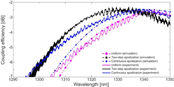
The experimental results are presented in Figs. 6-8. These include the uniform, the two-step apodized, and the continuously apodized grating couplers in different layout configurations, specifically with a linear taper, a non-adiabatic taper, and a free-propagation region. The peak measured coupling efficiencies are −2.7 dB (54%) and −2.5 dB (56%), for the uniform and the apodized grating couplers, respectively. The impact of different coupler layout configurations on the fiber-chip coupling efficiency is observed to be negligible. However, compared to our theoretical predictions (FDTD), the experimental coupling efficiency is about 0.3 dB (~4%) smaller for a uniform grating coupler. For the apodized couplers, the coupling loss penalty is found to be 0.9 dB (~13%). Furthermore, as it can be observed in Figs. 6(a), 7(a), and 8(a), the measured spectral response for all fabricated structures is shifted by ~40 nm towards longer wavelengths. The observed coupling loss penalty and the spectral shift is attributed to the fabrication imperfections, specifically a fabrication bias of ~40 nm compared to the nominal design dimensions, as confirmed by SEM inspection and the FDTD calculations carried out for the biased structures (Fig. 9).
Fig. 6. (a) Measured coupling efficiency as a function of wavelength for the uniform, the two-step apodized, and the continuously apodized grating couplers with a linearly tapered access waveguide. (b) SEM image of the grating coupler. Detail views of the fabricated structures: (c) uniform, (d) two-step apodized, and (e) continuously apodized grating couplers.
Fig. 7. (a) Measured coupling efficiency as a function of wavelength for the uniform, the two-step apodized, and the continuously apodized focusing grating couplers with a non-adiabatic access waveguide. (b) SEM image of the coupler. Detail view of the fabricated structures: (c) uniform, (d) two-step apodized, and (e) continuously apodized focusing grating couplers.
Fig. 8. (a) Measured coupling efficiency as a function of wavelength for the uniform, the two-step apodized, and continuously apodized focusing grating couplers with a free-space region. (b) SEM image of the coupler. Detail view of fabricated structures: (c) uniform, (d) two-step apodized, and (e) continuously apodized grating couplers.
The measured spectral response exhibits a small ripple with a magnitude in the range of 0.2 - 0.6 dB (3 – 6%) for different grating geometries and layout configurations. The ripple is attributed to the back-reflections at the interface between the access taper waveguide and the grating region, and the reflection at the fiber facet. From the magnitude of the Fabry-Perot fringes, we estimate that the lower back-reflections (~3%) are achieved for curved grating couplers (uniform and apodized gratings, see Figs. 7(a) and 8(a)), while the reflections for the linearly-tapered grating couplers are about 6% (see Fig. 6(a)). The influence of the
back-reflections can be effectively mitigated by established techniques such as curving and offsetting the grating lines [41].
In Fig. 9, we compare our experimental results with calculated spectral responses for different grating coupler designs with biased structural dimensions, as measured by SEM. A good agreement is observed between the measurement and simulation results.
Fig. 9. Calculated and measured coupling effiency as a function of wavelength for the uniform, the two-step apodized, and the continuously apodized grating couplers. Here, the simulation results include the influence of 40 nm fabrication bias, as determined by the SEM inspection.
It is worth noting that albeit the measured coupling efficiency is 0.3 - 0.9 dB (4 – 13%) lower compared to the peak theoretical efficiency (because of the fabrication bias discussed above), these results still compare favorably with the previously reported 1.3 μm surface grating couplers, while the latter also demand multiple etch steps [26–28], custom-designed silicon wafers [26], or non-standard SOI thickness [27].
4. Grating coupler with a backside reflector
As we have shown, the coupling angle optimization and grating apodization using SWG effective medium engineering can be efficiently used to substantially increase the fiber-chip coupling efficiency. The main limiting factor which remains is the leakage loss to the silicon substrate through the BOX layer [3,7]. Presently, three main approaches have been used to circumvent this limitation [6,14–20]. The first approach requires a specialized SOI platform with the dielectric (Bragg) reflector [18,20]. The second approach employs backside wafer metallization, which includes removing the silicon handle substrate by local etching, followed by metal mirror deposition step [14–17]. In the third approach, grating intrinsic directionality is increased (>95%) by blazing effect [23,25]. Here, we numerically investigate the second approach (backside metal processing) to potentially further increase the coupling efficiency of the coupler structures developed in this work. Specifically, we have carried out FDTD calculations of the nominal designs for the uniform, the two-step apodized, and the continuously apodized couplers presented in Section 2 with the metal mirror implemented underneath the grating, as schematically shown in the inset of Fig. 10. The FDTD simulation results are shown in Fig. 10 for all nominal grating coupler designs. The peak coupling efficiency of –1.71 dB (68%) is predicted for a uniform grating coupler, while the sub-decibel coupling performance is predicted for the apodized surface grating couplers. The two-step apodized design shows a calculated efficiency of −0.7 dB (85%), while the efficiency of −0.5 dB (89%) is predicted for the continuously apodized design.
Fig. 10. Calculated coupling effiency as a function of wavelength for the uniform, the two-step apodized, and the continuously apodized grating couplers with a bottom metal mirror. Inset: Cross-section schematics (vertical cut) of the surface grating coupler with a bottom metal mirror.
5. Conclusion
We reported on the design and experimental characterizations of the surface grating couplers implemented in a standard 220 nm SOI substrate, for datacom wavelength region near 1.3 μm. By exploiting the concept of subwavelength grating refractive index engineering, both the coupler and the interconnecting waveguides were fabricated using a single etch process. The peak coupling efficiencies of −2.7 dB (54%) and −2.5 dB (56%) were measured for uniform and apodized surface grating couplers, respectively. Furthermore, by utilizing the metal reflector underneath the grating couplers, the peak fiber-chip coupling efficiency of up to −0.5 dB (89%) is predicted by FDTD calculations for our apodized design. These results open up promising prospects for the development of highly-efficient input/output optical coupling interfaces for silicon-based photonic integrated circuits for O-band optical communications.
Acknowledgment
This work was supported by the Slovak Research and Development Agency (SRDA) under the project APVV-0025-12, by the National Research Council Canada, and by the European Research Council (ERC) under the European Union’s Horizon 2020 research and innovation program (ERC POPSTAR - grant agreement No 647342).