K.A. Rzepiejewska-Malyska,a)G. Buerki, and J. Michler
Swiss Federal Laboratories for Material Testing and Research—EMPA, CH-3602 Thun, Switzerland
R.C. Major, E. Cyrankowski, S.A.S. Asif, and O.L. Warren
Hysitron, Inc., Minneapolis, Minnesota 55344 (Received 18 December 2007; accepted 7 April 2008)
In nanoindentation, the occurrence of cracks, pileup, sink-in, or film delamination adds additional complexity to the analysis of the load–displacement curves. Many
techniques and analysis methods have been used to extract both qualitative and quantitative information from the indentation test both during and after the test. Much of this information is obtained indirectly or may even be overlooked by current testing methods (e.g., cracks that open only during the loading cycle of the test may go unnoticed from a typical residual indentation analysis). Here we report on the development of a miniature depth-sensing nanoindentation instrument and its
integration into a high-resolution scanning electron microscope. Real-time observation of the nanoindentation test via scanning electron microscopy allows for visualization and detection of certain events such as crack initiation, pileup, or sink-in, and other material deformation phenomena. Initial results from aluminum 〈100〉 and a thin gold film (∼225 nm) are presented.
I. INTRODUCTION
Nanoindentation is one of the most widely used tech-niques for mechanical characterization of thin-film coat-ings and nanostructured materials.1The standard nanoin-dentation test yields a force–displacement curve from which the mechanical properties of the tested material can be extracted. The onset of plastic deformation in addition to hardness and elastic modulus of the material are examples of information obtained in a standard na-noindentation experiment. Fracture behavior may be as-sessed by analyzing the crack length and the residual imprint left in the sample. This can give insight into the fracture toughness of the sample. Other material defor-mation behavior such as pileup or sink-in and thin-film delamination may be observed as well. Traditionally, these phenomena have been characterized only upon analysis performed after the nanoindentation test has been completed. Until recently, correlation of events that accompany material deformation (such as cracking, de-lamination, and microstructural changes) with the corre-sponding features in the force–displacement curve has been largely based on educated speculation. The devel-opment of quantitative, in situ, nanoindentation tools are
a necessity for providing conclusive support for many of the proposed theories and models used to explain many of the material deformation processes that occur during the nanoindentation test.
Recent work by Minor et al. involving quantitative nanoindentation experiments inside a transmission elec-tron microscope (TEM) illustrates the power of coupling real-time electron imaging with nanoindentation.2 This work led to new insights into the onset of plastic defor-mation in materials. In 1968, Gane and Bowden reported on one of the first integrations of an indentation-type device into a scanning electron microscope (SEM).3 Other groups followed along in later years with SEM integrations as well.4,5 More recently, Rabe et al. inte-grated a microindentation device inside a SEM.6The in situ SEM imaging during the microindentation test pro-vided a real-time monitor of the true contact area, pileup, and shear band formation7 throughout the indentation cycle. Another advantage of in situ SEM indentation is the capability to observe crack initiation and time-correlate this event to the force–displacement curve. Other experiments that would be ideally suited for the SEM nanoindentation technique include bending/ deformation of nanowires as well as nanopillar and nano-sphere compression among many others.
The development of a quantitative nanoindentation system integrated into a high-resolution SEM is dis-cussed here. The design principles are somewhat similar
a)
Address all correspondence to this author. e-mail: [email protected] DOI: 10.1557/JMR.2008.0240
to the instrument introduced elsewhere; however, there are some significant differences.6The main differences are the electrostatic force actuation, capacitance displace-ment sensing, load resolution, the imaging resolution, and two possible indentation control modes (open-loop load ramp or closed-loop displacement ramp) available as well as the size of the current design. A Hysitron PicoIndenter transducer8
(Minneapolis, MN) provides high-sensitivity force–displacement data and a Hitachi
S-4800 (Japan) SEM provides high-resolution imaging. This novel instrument for in situ observation has a large number of applications due to its design flexibility, which allows for sample/indenter rotation and tilt with respect to the imaging axis.
To show the potential of this technique, we performed in situ nanoindentation tests on two materials that have been widely investigated in the literature. Initial results obtained from an aluminum 〈100〉 single crystal and a thin gold film (∼225 nm) deposited on a fused quartz substrate showed interesting material deformation and delamination behavior.
II. EXPERIMENTAL
A. Integration of the nanoindenter into the SEM There are several requirements that have to be fulfilled by the instrument to be SEM compatible. Material selec-tion is crucial for successful integraselec-tion into the SEM operating environment. The used materials must be non-ferromagnetic or rather cause low electromagnetic dis-turbance. Otherwise, they may influence the electron beam and cause distortions in the image. The operating pressure in the chamber is in the high-vacuum (HV) range. All materials used for construction were at a mini-mum HV if not ultrahigh-vacuum (UHV) compatible materials. The materials chosen for the support structure and main design elements were titanium, copper, and aluminum. Machinable ceramic (Macor) and vacuum-compatible epoxy were used for electrical isolation.
Modern high-resolution SEMs often have small vacuum chambers to minimize vibrations and limit the vacuum pump-down time. This puts a severe size con-straint on the indenter hardware. The entire nanoindenter including motion stages, support structure, and sample stage were miniaturized so they could be inserted through the load-lock and fit inside the chamber. Due to the size restrictions of operating inside the SEM, a quan-titative miniaturized force–displacement transducer was
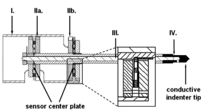
used. This transducer was originally developed for in situ TEM applications where space is even more constricted.2 The transducer is capable of independent electrostatic force actuation and capacitance-based displacement sensing. The miniature transducer comprises two sensor cores, one configured as a force actuator (Fig. 1, IIb) and the other as a displacement sensor (Fig. 1, IIa). Both
cores are of the three-plate capacitor design, i.e., a spring suspended center plate (center electrode) occupies the space between two fixed outer plates (outer electrodes). A dielectric is used to space the plates such that they are nominally parallel. The two sensor cores are attached together by a central rod (Fig. 1, III) connecting the center plates such that they always move together. The rod (Fig. 1, III) extends from the opposite face of the center plate of one core. An indentation tip holder (Fig. 1, IV) screws onto a threaded rod that extends from the end of the central connecting rod. The connecting rod (Fig. 1, III) and the tip holder (Fig. 1, IV) are parts of a conduction path for dissipating charge from the tip when the tip is impinged on by the electron beam of the SEM. The electrically conductive tip used thus far is made of boron-through-doped diamond. A cube corner tip geom-etry was chosen for the experiments presented here. This geometry allows for easy observation of the indenter sur-roundings during the experiment.
Electrostatic actuation of the nanoindenter probe is realized by applying a known voltage between the mov-able center plate and the tip-side fixed outer plate of the force actuator sensor core (Fig. 1, IIb). In general, the electrostatic force Fegenerated by an actuatable parallel-plate capacitor is described by
Fe= o 共1 − ␦Ⲑdo兲2V
2
, (1)
whereois the zero-volt (resting) electrostatic force con-stant, dois the zero-volt (resting) electrode gap,␦ is the displacement of the center electrode away from do, and V is the voltage applied across the center plate and the tip-side outer plate. During the indentation test, the elec-trode gap dimension changes. This has an effect on the scaling between Fe and V
2
and thus on the true applied electrostatic force. Equation (1) takes into account this electrode gap change during indentation.
Displacement sensing is done using a differential ca-pacitance half-bridge method involving a high-frequency
FIG. 1. Cross-sectional view of the actuatable capacitive transducer: I, transducer body; II, multiplate capacitor (inset: magnified view) (a) for displacement measurement and (b) for load actuation; III, conductive threaded rod; and IV, conductive probe.
(∼150 kHz) signal on one fixed outer plate of the dis-placement sensor core and a second signal of the same frequency but phase shifted by 180° on the other fixed
outer plate of the same core. These signals are high enough in frequency relative to the mechanical band-width of the transducer to not actuate it. In the absence of stray capacitance, the transfer function for the displace-ment signal is:
Vout Vac =C2 − C1 C1 + C2 =␦ d¯ , (2)
where Vacis the equal amplitude of the two applied high-frequency signals, Vout is the voltage output from the center plate of this core, and d¯ is the mean electrode gap of this core. The voltage output from the center plate will be of the same frequency as the applied high-frequency signals, and its phase (0 or 180°) will be dictated by
whichever of the two capacitances, C1or C2, is larger. The SEM nanoindentation instrument uses a digital signal processor (DSP) based feedback control system in communication with a computer through a universal se-rial bus (USB) link. This approach was preferred over traditional data acquisition hardware to eliminate plug-in data acquisition cards internal to the computer and to increase portability. The DSP architecture is flexible and ideally suited to handle the real-time data acquisition and control processes of the instrument. In its current con-figuration, the control system operates in two modes: (i) open-loop load ramp where a predetermined “total
ap-plied load” (actually V2) versus time function is estab-lished and (ii) displacement control with a displacement set point versus time ramp. The load applied to the sample is the difference between the total applied load (the electrostatic force) and the force required to displace the springs internal to the transducer (k␦ where k is the effective spring constant of the internal springs). The second mode is a closed-loop mode that uses a propor-tional–integral–derivative (PID) loop to maintain the
pre-determined displacement versus time ramp. When oper-ating in the displacement-control mode, the controller also provides for active damping of system vibrations, which is advantageous for the inherently low-damping vacuum environment.
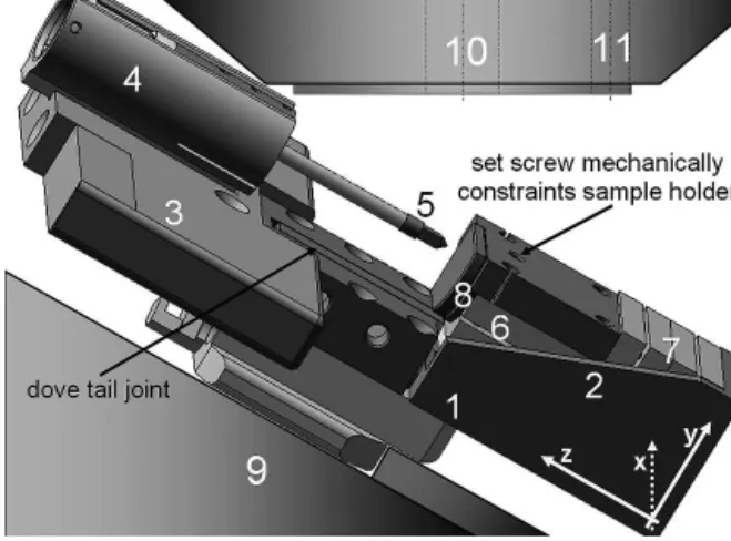
Figure 2 shows the overall computer-aided design (CAD) of the instrument. The main frame is made of titanium, and its lower part (Fig. 2, no. 1) provides sup-port for the x, y (Fig. 2, no. 7) and z (Fig. 2, no. 6) piezoactuators (SmarAct, Oldenburg, Germany) that are used for lateral sample positioning (x, y) and coarse tip-sample approach (z). The slip-stick piezoactuators allow for positioning within an accuracy of 50 nm and have a travel range of several mm. The coarse approach mode is able to bring the tip to within ∼100 nm of the sample surface. Prior to executing the indentation cycle, the
force–displacement transducer serves as a fine-approach
actuator and brings the tip into initial contact with the sample. The maximum total displacement for the fine approach and indentation cycle is currently 5 m. To achieve high structural rigidity, the lower part of the main frame (Fig. 2, no. 1) is supported by a rib on one side (Fig. 2, no. 2). The bending moment, which is a result of the weight of the instrument as well as the force applied during the indentation test, is concentrated at this point. The sample holder (Fig. 2, no. 8) is supported by a plate to minimize compliance during the indentation test. The shaft of the sample holder is keyed, and a mechani-cal stop prevents rotation during the indentation cycle. A set screw mechanically constrains the sample holder and locks it in place, preventing additional movement. A con-ductive silver paste is used for affixing samples to the sample holder to avoid sample charging, which can dra-matically reduce SEM image resolution. To facilitate quick and easy tip and sample replacement, the main frame was made in two pieces (lower and upper parts) joined with an adjustable dovetail joint and secured by two set screws. The adjustable dovetail joint also allows for manual adjustment of the distance between the end of the tip and the sample. This accommodates samples of varying heights between 0 to 10 mm.
The upper part of the main frame (Fig. 2, no. 3) has two design functions: (i) provide support for the force–
displacement transducer and associated electronic circuit boards and (ii) allow for proper relative positioning of the tip and the sample. The support for the force–
displacement transducer is designed to fix the position of
FIG. 2. CAD image of the Hysitron force–displacement transducer
integrated inside the Hitachi S-4800 high-resolution SEM. The X-Y-Z coordinate system is related to the PicoIndenter. Note the transducer/ sample is tilted off-axis to allow SEM imaging of the sample surface during the indentation cycle. The numbers in the image correspond to the following components: 1, lower part of the main frame; 2, porting rib; 3, upper part of the main frame; 4, transducer in its sup-port; 5, conductive indenter probe; 6, z slip-stick actuator; 7, x, y slip-stick actuators; 8, removable sample holder; 9, SEM stage; 10, SEM electron gun; and 11, SEM high-magnification detector.
the transducer, protect it against the electromagnetic field, and prevent mechanical interference with the other internal components of the SEM.
B. Instrument calibration
The force–displacement transducer is precalibrated via
dead weights and laser interferometry to determine the effective spring constant k, the displacement sensitivity, the load sensitivity, and an initial estimate of the elec-trostatic actuation parameters. Before indentation experi-ments and at regular intervals, the zero-volt electrostatic force constantoand the zero-volt electrode gap do are refined by performing a large displacement (>3m) “air-indent” with the tip well removed from the sample (Fe⳱
k␦ must hold true at all data points in this situation).
Refining the calibration of the electrostatic actuation pa-rameters is crucial because the initial position of the cen-ter plate of the force actuator is affected by the tilt angle of the entire nanoindenter in the SEM, which affects both o and do values.
Two other important factors known to influence na-noindentation results are the machine compliance of the instrument and the tip area function calibration; however, neither has been quantified yet. The primary interest at this stage of the development is to conduct phenomeno-logical studies rather than to determine hardness and elastic modulus. In regard to identifying the potentially significant sources of machine compliance, finite ele-ment analysis of the main frame is currently underway, and the overall compliance of the slip-stick actuators used for positioning is currently being evaluated. As for the tip-area function calibration, an attractive option would be to take advantage of the in situ imaging capa-bility of the SEM to provide a direct measurement of the projected contact area at each point of the indentation test. This would allow one to account for pileup or sink-in as well as fracture. The traditional Oliver and Pharr9 analysis is not able to directly account for these phenom-ena.
III. RESULTS AND DISCUSSION A. In situ instrument performance
The performance of the force–displacement transducer
as well as SEM-related factors influence the overall per-formance of the system. Important factors include the noise level of the transducer, SEM resolution, sample/tip contamination, charging during SEM imaging, and sys-tem vibrations. The force–displacement transducer has a
maximum load of∼1500 N, a load noise floor (RMS) of ∼0.1 N, a maximum displacement of 5 m, and a dis-placement noise floor (RMS) of ∼0.4 nm. The micro-scope used for integration is a high-resolution Hitachi S-4800 scanning electron microscope. SEM resolution is
strongly dependent on the sample material properties (e.g., conductive, semiconductive, or insulative) and the atomic mass of the studied materials. A conductive, boron-through-doped diamond tip having a cube corner geom-etry was used for the nanoindentation tests. Both the tip and the sample were grounded to suppress charging. Nevertheless, contact between the tip and the sample often caused a change in image contrast and image reso-lution in the material around the indent. This is due to local charging and subsequent charge dissipation/ redistribution resulting from the tip-sample contact. Con-tamination caused by prolonged exposure of the tip and the sample to the electron beam also must be minimized. Carbon deposition on the tip and the sample can result in reduced image resolution.
B. In situ nanoindentation
Initial data from two different materials are shown below to illustrate the system performance. Interesting observations were obtained from an aluminum 〈100〉 single crystal and a thin gold film (∼225 nm) sputter coated onto a fused quartz substrate. Figure 3 shows two load–displacement curves for aluminum, one taken under
displacement control [Fig. 3(a)] and the other under open-loop load control [Fig. 3(b)]. The load-drop and pop-in events mostly result from dislocation bursts2 oc-curring in the sample volume beneath the probe during displacement-controlled or open-loop load-controlled na-noindentation, respectively.
As has been shown previously, the displacement-control mode tends to be more sensitive to discrete events10
as indicated by the clear load drops in Fig. 3(a). The first dramatic load-drop event occurred around 20 N in the case of the displacement-controlled test. This load-drop event may be correlated with breaking through an outer layer atop the substrate,11although dis-location activity in the aluminum is likely to accompany this event. Note how the load drops to negative values after the initial breakthrough event. This is most likely caused by the exposure of bare aluminum, which has a much higher surface energy than the oxide outer surface and results in a significant adhesive interaction.2A simi-lar transition from oxide-indenter to metal-indenter interaction was seen during displacement control mode indents on indium.10 The adhesive interaction may be further enhanced by the relatively clean vacuum environ-ment and minimal water adsorption layers. The large adhesive force observed upon unloading also is indica-tive of a bare-metal–indenter interaction.
For comparison, the same type of experiment was per-formed in the open-loop load-control mode with which pop-in events12were observed [Fig. 3(b)]. This behavior was confirmed by the SEM video recording taken during this experiment, which showed the indenter tip making a sudden jump into the material13
pileup or sink-in was observed within the resolution lim-its of the SEM. The outer layer material was often found to delaminate from the aluminum and adhere to the in-denter tip [see Fig. 3(b) insets]. This illustrates the need for in situ observation to detect, observe, and correct for these events.
Thin gold films are often used as substrates for the formation of self-assembled monolayers and other mo-lecular thin films.14,15
Gold is inert, yet can be easily modified through the chemisorption of molecules con-taining a thiol or disulfide functional group. The rough-ness of the gold film as well as adhesion to the underly-ing substrate can be critical to achievunderly-ing the ultimate goal of a well-characterized functional surface used for a va-riety of applications (e.g., molecular/organic electronics, biofunctional surfaces). Gold films have also been used as electrodes in electrochemical studies and applica-tions.16The gold film can be evaporated onto the quartz surface of a quartz crystal microbalance. A thin metallic layer (e.g., titanium or chromium) is often used to pro-mote the adhesion of metallic layers to the underlying substrate. Without the adhesion layers, the films are often only weakly adsorbed and can easily delaminate, limiting the practical use of the films. However, this adhesion layer can lead to deleterious effects such as influencing the surface roughness or actually dissolve into solution under certain potentials as was shown by Hoogvliet and van Bennekom.16
Figure 4 shows the results from in situ SEM nanoin-dentation on a sample consisting of a thin gold film (∼225 nm) sputter coated onto a fused quartz substrate. No interfacial layer was used to promote adhesion of the gold film to the substrate. The absence of the adhesion layer resulted in a weak interfacial bond as was evident from the data. The nanoindentation test was performed under displacement control (see the movie in the supple-mental information). There was significant adhesion
be-tween the tip and the indented material as indicated in the load–displacement curve [Fig. 4(a) inset], similar to the
aluminum data shown previously. The tip–sample
adhe-sion was strong enough to cause delamination of the film from the substrate. The SEM images in Figs. 4(d) and 4(e) suggest that the film actually lifts off of the substrate and then releases from the tip. The real-time movie of this indentation provides a better depiction of the delami-nation event than the still images alone (see the movie in the supplemental information). This delamination event explains the discontinuous shape of the unload portion of the load–displacement curve shown in the inset of
Fig. 4(a). Further evidence for this mechanism would require the time-consuming process of obtaining a cross section of the residual indent to visualize the interfacial crack. The in situ SEM observation provided clear evi-dence of film delamination and allowed for accurate in-terpretation of the load–displacement curve. Without the
SEM observation, one may erroneously interpret the load–displacement curve as simple adhesion between
the tip and film. This is a clear example of the utility provided by the real-time imaging in concert with the load–displacement data.
IV. CONCLUSION
The SEM nanoindentation system described previ-ously illustrates the power of combining quantitative load–displacement measurement with real-time SEM
im-aging. On the aluminum〈100〉 sample, the oxide break-through event was observed in real-time and easily time correlated to the pop-in event observed in load–
displacement curves. On the gold film sample, the nega-tive load values and the discontinuity observed in the load–displacement data could be accurately attributed to
tip/sample adhesion and film delamination. The real-time imaging provided clear evidence of this mechanism.
FIG. 3. In situ SEM nanoindentation of an aluminum 〈100〉 single crystal. Load–displacement curves acquired in two different modes: (a) displacement control mode and (b) open-loop load control mode. The insets in (b) are the SEM images that correspond to the indicated points on the load–displacement plot and demonstrate a rapid change in the indentation depth caused by breaking through the outer layer. The circles
Educated speculation about the cause of certain fea-tures in the indentation curve may now be supported by simultaneous imaging of the nanoindentation test. The use of high spatial resolution, real-time imaging provides accurate nanopositioning capabilities. In situ testing pro-vides valuable insight into phenomena such as pileup or sink-in, delamination, and other material deformation be-havior that may occur during nanoindentation experi-ments. The SEM imaging also allows for the precise positioning of the indenter probe and selection of a defect free location for the indentation test. This instrument is an ideal tool for the characterization of particularly chal-lenging nanostructured materials such as nanowires, nanopillars, and nanospheres, where instrumentation re-quirements (i.e., force/displacement resolution, accuracy of the positioning system, and high magnification capa-bilities) are extremely important.
ACKNOWLEDGMENTS
The authors thank T.J. Wyrobek for supporting the project. We are grateful to S. Hoesli and E. Pieper for help and discussions regarding design and vacuum com-patibility of mechanical parts and for machining some of them, and to K. Wasmer for fruitful discussions. The force–displacement transducer and associated controller/
software were developed under a United States Depart-ment of Energy SBIR grant (No. DE-FG02-04ER83979)
awarded to Hysitron, Inc. We thank Swiss State Secre-tariat for Education and Research, EU FP6 project MASMICRO (No. 03.0225, NMP2-CT-2004-500095) for additional financial support.
REFERENCES
1. A.C. Fisher: Cripps: Nanoindentation (Springer-Verlag, New York, 2002).
2. A.M. Minor, S.A.S. Asif, Z. Shan, E.A. Stach, E. Cyrankowski, T.J. Wyrobek, and O.L. Warren: A new view of the onset of plasticity during the nanoindentation of aluminum. Nature Mat.5, 697 (2006).
3. N. Gane and F.P. Bowden: Microdeformation of solids. J. Appl. Phys.39, 1432 (1968).
4. H. Bangert and A. Wagendristel: Ultralow-load hardness tester for use in a scanning electron microscope. Rev. Sci. Instr.56(8), 1568 (1985).
5. H. Bangert and A. Wagendristel: Ultralow load hardness testing of coatings in a scanning electron microscope. J. Vac. Sci. Technol. 4(6), 2956 (1986).
6. R. Rabe, J-M. Breguet, P. Schwaller, S. Stauss, F-J. Haug, J. Patscheider, and J. Michler: Observation of fracture and plastic deformation during indentation and scratching inside the scanning electron microscope. Thin Solid Films206, 469 (2004). 7. J. Michler, R. Rabe, J-L. Bucaille, B. Moser, P. Schwaller, and
J-M. Breguet: Investigation of wear mechanisms through in situ observation during microscratching inside the scanning electron microscope. Wear259, 18 (2005).
8. O.L. Warren, S.A.S. Asif, E. Cyrankowski, and K. Kounev: U.S. Patent Application No. 20070180924 (filed Feb 7, 2007). FIG. 4. In situ SEM nanoindentation of a thin gold film (∼225 nm) deposited on fused quartz. The complete load–displacement curve is shown in (a). Images (b–f) were taken from the SEM movie recorded during the indentation test and correspond to the numbered points shown in the
curve (a). (b) I corresponds to the initial point of contact; (c) II maximum load; (d) III delamination of the coating from the substrate; (e) IV immediately after film delamination; and (f) V high-resolution image of the residual indent. The reference line and arrows are used to help distinguish the lift-off of the gold film.
9. W.C. Oliver and G.M. Pharr: An improved technique for deter-mining hardness and elastic modulus using load and displacement sensing indentation experiments. J. Mater. Res.7, 1564 (1992). 10. O.L. Warren, S.A. Downs, and T.J. Wyrobek: Challenges and
interesting observations associated with feedback-controlled na-noindentation. Z. Metallkd.95, 287 (2004).
11. W.W. Gerberich, J.C. Nelson, E.T. Lilleodden, P. Anderson, and J.T. Wyrobek: Indentation induced dislocation nucleation: The initial yield point. Acta Mater.44, 3585 (1996).
12. Y. Shibutani, T. Tsuru, and A. Koyama: Nanoplastic deformation of nanoindentation: Crystallographic dependence of displacement bursts. Acta Mater.55, 1813 (2007).
13. B. Moser, J. Kuebler, H. Meinhard, W. Muster, and J. Michler: Observation of instabilities during plastic deformation by in situ SEM indentation experiments. Adv. Eng. Mat.7(5), 388 (2005). 14. R.G. Nuzzo and D.L. Allara: Adsorption of bifunctional organic
disulfides on gold surfaces. J. Am. Chem. Soc.105, 4481 (1983). 15. A. Ulman: An Introduction to Ultrathin Organic Films from Lang-muir-Blodgett to Self-Assembly (Academic Press, San Diego, CA, 1991).
16. J.C. Hoogvliet and W.P. van Bennekom: Gold thin-film elec-trodes: An EQCM study of the influence of chromium and tita-nium adhesion layers on the response. Electrochim. Acta47(4), 599 (2001).