HAL Id: hal-03024869
https://hal.archives-ouvertes.fr/hal-03024869
Submitted on 26 Nov 2020
HAL is a multi-disciplinary open access
archive for the deposit and dissemination of
sci-entific research documents, whether they are
pub-lished or not. The documents may come from
teaching and research institutions in France or
abroad, or from public or private research centers.
L’archive ouverte pluridisciplinaire HAL, est
destinée au dépôt et à la diffusion de documents
scientifiques de niveau recherche, publiés ou non,
émanant des établissements d’enseignement et de
recherche français ou étrangers, des laboratoires
publics ou privés.
Lasing up to 380 K in a sublimated GaN nanowire
S. Sergent, B. Damilano, S. Vézian, S. Chenot, T. Tsuchizawa, M. Notomi
To cite this version:
S. Sergent, B. Damilano, S. Vézian, S. Chenot, T. Tsuchizawa, et al.. Lasing up to 380 K in a
sublimated GaN nanowire. Applied Physics Letters, American Institute of Physics, 2020, 116 (22),
pp.223101. �10.1063/5.0004771�. �hal-03024869�
Lasing up to 380 K in a sublimated GaN nanowire
S. Sergent,
1,2B. Damilano,
3,a)S. Vézian,
3S. Chenot,
3T. Tsuchizawa,
1,4and M. Notomi
1,2,b) 1Nanophotonics Center, NTT Corp., 3-1, Morinosato Wakamiya Atsugi, Kanagawa 243-0198, Japan
2NTT Basic Research Laboratories, NTT Corp., 3-1, Morinosato Wakamiya Atsugi, Kanagawa 243-0198, Japan 3Université Côte d’Azur, CNRS, CRHEA, Rue B. Grégory, 06560 Valbonne, France
4NTT Device Technology Laboratory, NTT Corp., 3-1, Morinosato Wakamiya Atsugi, Kanagawa 243-0198, Japan
We report on GaN nanowire lasers fabricated by selective-area sublimation and we show that sublimated GaN nanowires can exhibit ultraviolet lasing action under optical pumping beyond room temperature, up to 380 K. We study by microphotoluminescence the temperature-dependent behavior of single nanowire lasers between 7 K and 380 K and extract a characteristic temperature T = 126 K. We finally present a statistical study of the maximum lasing temperature in individual sublimated GaN nanowires and use it to assess the performance of the selective-area sublimation method for nanowire-based lasing applications.
a) E-mail: bd@crhea.cnrs.fr
b) E-mail: masaya.notomi.mn@hco.ntt.co.jp
Group-III nitrides have been established as the key material for a range of practical light-emitting devices and mass-consumption optoelectronics owing to their unique optoelectronic properties: efficient emitting processes up to high-temperatures and a large accessible spectral range from ultraviolet to visible wavelengths. Building on the strengths of this semiconductor compound family, the research community has recently focused on GaN nanowires (NWs) to realize even more advanced optoelectronic and photonic devices with new functionalities, higher efficiency, smaller footprint or lower energy cost: e.g. flexible light-emitting diodes [1], single photon sources [2,3] or even photon [4-8], plasmon [9-11] and polariton nanolasers [12]. Most GaN nanowires are now realized in the frame of bottom-up epitaxial processes based either on molecular beam epitaxy [13-15] or on metal-organic chemical vapor deposition [15-17]. Using bottom-up epitaxial techniques, it remains however challenging to reach a precise control of the structural properties, geometry and position of GaN NWs all at once. Alternatively, several top-down fabrication techniques have been proposed to circumvent such difficulties: (i) the dry etching of a GaN epilayer followed by the wet chemical cleaning of damaged sidewalls [4,6] and (ii) the selective-area sublimation of a GaN epilayer in ultra-high vacuum [18,19]. The latter method does not necessitate any post-processing cleaning and even allows for epitaxial regrowth straight after NW formation [18,20]. Most importantly, in the frame of the GaN sublimation method, we have shown that it is possible to achieve a fine control of the NW position, dimensions
and geometry on nano, micro and macro scales [8]. As a result, this method has led to the realization of various photonic elements operating at room-temperature such as metalenses [21], NW-induced photonic crystal nanocavities [8] and photonic nanolasers based on Fabry-Pérot resonances [7,8]. In this letter, we focus on photonic nanolasers in sublimated GaN NWs and we report on the temperature dependence of their lasing characteristics. In contrast to previous GaN NW lasing reports, we demonstrate lasing operation beyond room-temperature, up to a temperature T = 380 K well suited for practical device applications in high-temperature environment. This impressive result confirms the high structural and optical quality of GaN NWs obtained by the selective area sublimation method.
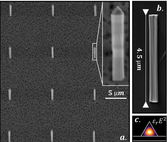
The GaN NW sample investigated in this work is similar to the one described in reference [8]. The base material is a GaN/AlGaN/GaN epilayer stack deposited on sapphire by ammonia-based molecular beam epitaxy. The nominal thickness of the upper GaN layer is 4.5 microns and determines the NW length. The epistack is then covered by a 60 nm SiN hard mask and arrays of nanopatterns are defined in the mask by electron beam lithography and reactive ion etching. The subsequent sublimation process is performed within the molecular beam epitaxy reactor at an ultra-high vacuum level and leads to the formation of arrays of GaN NWs presenting triangular sections (Fig. 1a). The SiN hard mask is then removed in a hydrofluoric acid solution at room temperature. Prior to the lasing experiments, the NWs are transferred on a 108-nm-thick SiN layer deposited on Si (100) (see reference [22] for fabrication details), which ensures good optical confinement and heat transfer (Fig. 1b). We should note that the triangular section base of investigated NWs ranges between 180 nm and 550 nm (see Table S1 in Supporting Information). Such dimensions are beyond the photonic cutoff in the near ultraviolet range [8] and all NWs are thus expected to support guided modes with confinement factors ranging between 76% and 99% (Fig. 1c) and Fabry-Pérot resonances.
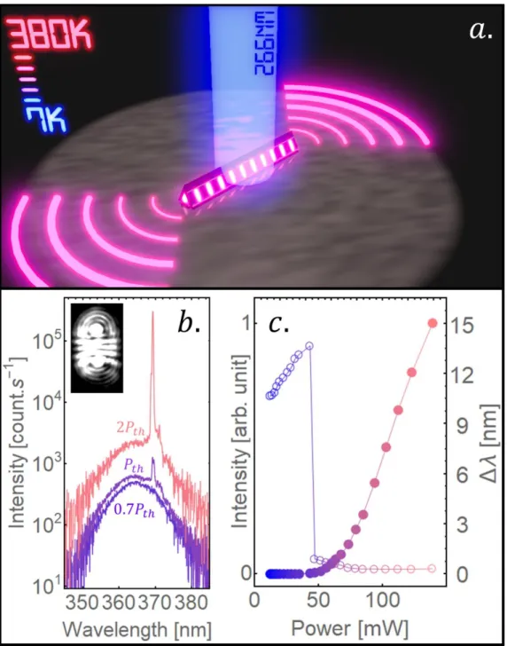
The SiN sample with the transferred GaN NWs is then attached to a heater connected to a temperature controller and placed in a continuous-flow He cryostat. In this apparatus, the sample temperature can be varied between 7 K and 380 K. The lasing experiments are carried out by microphotoluminescence in the configuration schematically represented in Fig. 2a, using a 266 nm Teem Photonics pulsed laser as the excitation source. The laser pulse width is 0.35 ns and its repetition rate is 1 kHz. The pump laser is focused at the center of the GaN NWs with a Mitsutoyo microscope objective dedicated to the ultraviolet range with a 0.42 numerical aperture and a 50 times magnification. The pump laser spot radius on the sample is estimated to be 1 µm. The light emitted by the excited NW is collected
by the objective in a confocal geometry and the signal is focused through a 50 micron slit on an ultraviolet-enhanced CCD camera after dispersion of the signal on a 600 grooves/mm grating. The spectral resolution is 200 pm. For imaging purposes, the signal can be instead focused on an ultraviolet CMOS camera after filtering out the 266 nm pump laser light.
We first carry out room-temperature microphotoluminescence experiments on the NW displayed in Fig. 1b, varying the peak pump power absorbed by the NW between 10 and 140 mW (the laser absorption ratio by the NW η = 8% is estimated by finite difference time-domain calculations). As can be seen in Fig. 2b, the low pump power spectra do not exhibit a clear Fabry-Pérot resonance peak due to the high GaN absorption in the band-edge vicinity. As the pump power increases, a resonant peak appears on the low energy side of the GaN emission at 𝜆 = 369 nm, its intensity exhibit a non-linear behavior as power increases whereas its linewidth narrows from 0.9 nm down to 0.26 nm (Fig. 2c). Those are clear evidence of lasing with a threshold 𝑃𝑡ℎ= 64 mW, as estimated from the light-light curve of Fig. 2c. Above threshold, the light emitted from the NW exhibit clear interference fringes that is an additional signature of lasing action (inset of Fig. 2b).
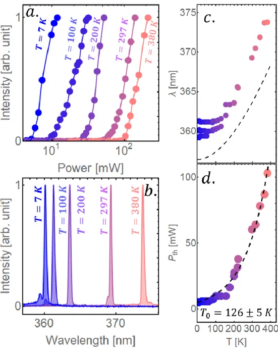
Such power-dependent experiments are then carried out on the same NW at temperatures ranging between 7 K and 380 K. It leads to similar non-linear light-light curves (Fig. 3a) with sharp and intense lasing modes above threshold (Fig. 3b). The NW laser however presents very different characteristics as a function of temperature in terms of the number of lasing modes, their wavelength and their threshold. First, at temperatures higher than 177 K we observe single mode lasing (Fig. 3b and c), but low temperature experiments reveal a competition between several modes as the pump power increases. (see Fig 3c and Fig. S1 in Supporting Information). The behavior is rather counterintuitive as the broadening of the gain with temperature usually triggers the appearance of multimode lasing in Fabry-Pérot NW lasers [23]. This suggests that the reduced gain level at higher temperatures compensates the effect of gain broadening and effectively limits the number of lasing modes in the investigated excitation range. Second, one can note that the lasing modes redshift as the temperature increases. The behavior does not closely follow the redshift of a single Fabry-Pérot resonance that is expected from the refractive index dependence on the temperature near the band-edge [24-25]. Instead, as the temperature increases one can observe clear jumps from mode to mode (notably around 150 K and 220 K) and the lasing wavelength redshifts along with the GaN band-edge (see dashed line in Fig. 3c). Third, because the non-radiative recombination rate increases and the gain spectrum broadens as temperature rises, the lasing threshold increases exponentially from 5 mW at 7 K up to 100 mW at 380
K (Fig. 3a and d). The latter constitutes the highest temperature reported to date in a NW laser. We extract from the temperature dependence of the lasing threshold the characteristic temperature of the laser 𝑇0= 126 ± 5 𝐾 (see dashed line in Figure 3d). This is somehow lower than values found in bulk GaN lasers: for example optically pumped strip lasers can show characteristic temperatures as high as 235 K [26]. The difference may be related to higher temperature-dependent non-radiative surface recombinations in the investigated nanolaser, an issue that could be addressed by adding a shell around the GaN core. We should note however that even without a shell, the characteristic temperature is already larger than core-shell semiconductor NW lasers with narrower bandgaps: in single core-shell AlGaAs-GaAs NW lasers the characteristic temperature is typically limited to 𝑇0= 109 ± 12 𝐾 [23].
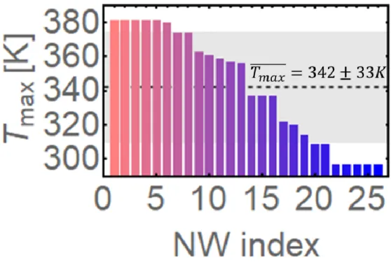
To further assess the quality of sublimated GaN NWs for lasing applications, we finally realize a statistical study of the maximum lasing operation temperature 𝑇𝑚𝑎𝑥 obtained in 26 different sublimated GaN NWs (Fig. 4). The dimensions and the maximum operation temperature of investigated NWs can be found in Supporting Information (Table S1). Owing to the acceleration of non-radiative recombination rates and the reduction of gain with temperature, less and less NWs can sustain lasing as the temperature increases. As a result, 24% of the NWs exhibit lasing action up to 380K and the set of 26 NW lasers presents a mean maximum operation temperature 𝑇̅̅̅̅̅̅ =𝑚𝑎𝑥 342 ± 33𝐾. The difference in 𝑇𝑚𝑎𝑥 from NW to NW may arise from variations in mode confinement, optical losses and non-radiative recombinations processes. First, the mode confinement in the Fabry-Pérot cavity is conditioned by the dimensions of the NW. This is however unlikely to have a major impact here because there is no clear correlation between 𝑇𝑚𝑎𝑥 and the NW geometry (see Table S1 in Supporting Information). Second, optical losses are dependent on the sharpness of the end-facets. Since one of the end-facets is defined during the dry NW transfer, there are large variations here. Sidewall fluctuations, which have been found to lie in the 3 nm to 32 nm range [8], have also a major role in optical loss variations. Third, with a threading dislocation density of about 5⨉109 cm-2 in the original two-dimensional epilayer, the number of threading dislocations may vary in each sublimated NW between 1 and 3. As a result, non-radiative recombinations processes at threading dislocations and their temperature dependence will also vary. Non-radiative recombination processes at the interface with air may also play a role here, as already mentioned. Let us note that in order to address the effect of non-radiative recombinations on the lasing characteristics two counter-measures can be taken: (i) a drastic reduction of the threading dislocation density in the original GaN by using dislocation filtering epistack designs or by growing the
epilayer on a group-III nitride homosubtrate, (ii) growing an AlGaN shell around the GaN NWs to inhibit non-radiative recombination processes at surface states. Regarding the effect of end-facets on optical losses, one can circumvent this problem by growing the NW material directly on the sapphire and use the refractive index contrast with the substrate at the bottom end-facet of the NW [6]: this configuration has the added advantage of allowing for integrated arrays of NW lasers and has already been demonstrated with sublimated GaN NWs [7]. One could alternatively use a bottom Bragg mirror, as often done in vertical-cavity surface-emitting lasers [27].
As a conclusion, we have demonstrated that GaN NWs fabricated by a top-down selective area sublimation method can give rise to lasing effects at temperatures as high as 380 K. This is larger than previously reported operation-temperatures in NW lasers [4-12,23,28] and it shows that sublimated GaN NWs are good candidates for practical lasing applications in a high-temperature environment without the need for an external cooling apparatus. Temperature-dependent measurements between 7K and 380 K showed however that GaN NW lasers can present a relatively low characteristic temperature 𝑇0= 126 ± 5 𝐾 and only a fraction (24%) of NWs actually lases up to 380 K. This means that there is still room for optimization of the NW lasers from both the material and optical design standpoints. We especially emphasized the importance that should be given in future works to (i) adding a shell around the GaN core, (ii) using higher quality GaN as the base NW material and (iii) using a vertical NW configuration with a bottom mirror. We should add that lower dimensionality emitters such as quantum disks and quantum dots that can readily be embedded in sublimated GaN NWs [8,18] should also improve their robustness against temperature.
This work has been supported by the JSPS KAKENHI Grant Number 15H05735 and the French National Research Agency (ANR) through the project NAPOLI (ANR-18-CE24-0022).
1. N. Guan, X. Dai, A. Messanvi, H. Zhang, J. Yan, E. Gautier, C. Bougerol, F.H. Julien, C. Durand, J. Eymery and M. Tchernycheva, ACS Photonics 2016, 3, 597-603.
2. S. Deshpande, J. Heo, A. Das and P. Bhattacharya, Nature Communication 2013, 14, 1675. 3. M. Holmes, K. Choi, S. Kako, M. Arita and Y. Arakawa, Nano Lett. 2014, 14, 982-986.
4. Q. Li, J. B. Wright, W. W. Chow, T. S. Luk, I. Brener, L. F. Lester and G. T. Wang, Optics Express 2012, 20, 17873.
6. M. Behzadirad, M. Nami, N. Wostbrock, M. R. Z. Kouhpanji, D. F. Feezell, S. R. J. Brueck, T. Busani, ACS Nano 2018, 12, 2373-2380.
7. B. Damilano, P.-M. Coulon, S. Vézian, V. Brändli, J.-Y. Duboz, J. Massies, P. A. Shields, Appl. Phys. Express 2019, 12, 045007.
8. S. Sergent, B. Damilano, S. Vézian, S. Chenot, M. Takiguchi, T. Tsuchizawa, H. Taniyama and M. Notomi,
ACS Photonics 2019, 6, 3321-3330.
9. Y.-J. Lu, J. Kim, H.-Y. Chen, C. Wu, N. Dabidian, C. E. Sanders, C.-Y. Wang, M.-Y. Li, B.-H. Li, X. Qiu, W.-H. Chang; L.-J. Chen, G. Shvets; C.K. Shih and S. Gwo, Science 2012, 337, 450-453.
10. Q. Zhang, G. Li, X. Liu, F. Qian, Y. Li, T. C. Sum, C. M. Lieber and Q. Xiong, Nature Communications 2012, 5, 4953.
11. Y.-J. Lu, C.-Y. Wang, J. Kim, M.-Y. Lu, H.-Y. Chen, Y.-C. Chen, W.-H. Chang, L.-J. Chen, M. I. Stockman, C. K. Shih and S. Gwo, Nano Lett. 2014, 14, 4381-4388.
12. A. Das, J. Heo, M. Jankowski, W. Guo, L. Zhang, H. Deng and P. Battacharya, Phys. Rev. Lett. 2011, 107, 066405.
13. R. Songmuang, O. Landré, and B. Daudin, Appl. Phys. Lett. 2007, 91, 251902.
14. K. A. Bertness, N. A. Sanford, and A. V. Davydov, IEEE J. Sel. Topics in Quantum Electron. 2011, 17, 847-858.
15. B. Alloing, S. Vézian, O. Tottereau, P. Vennegues, E. Beraudo, and J. Zúñiga-Pérez, Appl. Phys. Lett. 2011, 98, 011914.
16. S. D. Hersee, X. Sum and X. Wang, Nano Lett. 2006, 6, 1808-1811. 17. K. Choi, M. Arita, and Y. Arakawa, J. of Cryst. Growth 2012, 357, 58-61.
18. B. Damilano, S. Vézian, J. Brault, B. Alloing and J. Massies, Nano Letters 2016, 16, 1863-1868.
19. B. Damilano, S. Vézian, M. Portail, B. Alloing, J. Brault, A. Courville, V. Brandli, M. Leroux and J. Massies J. of Cryst. Growth 2017, 477, 262-266.
20. X. Sun, P. Wang, B. Sheng, T. Wang, Z. Chen, K. Gao, M. Li, J. Zhang, W. Ge, Y. Arakawa, B. Shen, M. Holmes, and X. Wang, Quantum Engineering 2019, 1, e20.
21. G. Brière, P. Ni, S. Héron, S. Chenot, S. Vézian V. Brändli, B. Damilano, J.-Y. Duboz, M. Iwanaga and P. Genevet, Adv. Opt. Mater. 2019, 1801271.
22. S. Sergent, M. Takiguchi, T. Tsuchizawa, A. Yokoo, H. Taniyama, E. Kuramochi and M. Notomi, ACS
Photonics 2017, 4, 1040-1047.
23. B. Mayer, D. Rudolph, J. Schnell, S. Morkötter, J. Winnerl, J. Treu, K. Müller, G. Abstreiter, G. Koblmüller, and J. J. Finley, Nature Communications 4, 2931 (2013).
24. L. Siozade, S. Colard, M. Mihailovic, J. Leymarie, A. Vasson, N. Grandjean, M. Leroux and J. Massies, Jap. J.
Appl. Phys. 39, 20 (2000).
25. N. Watanabe, T. Kimoto and J. Suda, Jap. J, Appl. Phys. 51, 112101 (2012).
26. X. H. Yang, T. J. Schmidt, W. Shan, J. J. Song, and B. Goldenberg. Appl. Phys. Lett. 66, 1(1995).
27. G. Cosendey, A. Gastiglia, G. Rossbach, J.-F. Carlin and N. Grandjean, Appl. Phys. Lett. 104, 241113 (2014). 28. J. Tatebayashi, S. Kako, J. Ho, Y. Ota, S. Iwamoto, and Y. Arakawa.Nature Photonics 9, 501 (2015).
FIG. 1. a. 30°-tilted scanning electron microscope view of an array of GaN NWs fabricated by selective-area sublimation. The inset is a zoom on a single NW. b. Top-view of a triangular NW transferred on SiN. The base of the triangular section is 400 nm and the NW length is 4.5 µm. c. Simulation of the fundamental mode guided in the NW represented in panel b.
FIG. 2. a. Schematic representation of the lasing experiments. b. Room temperature photoluminescence spectra of the NW represented in Fig. 1b at various peak pump powers 0.7𝑃𝑡ℎ, 𝑃𝑡ℎ= 64 mW and 2𝑃𝑡ℎ. The inset is the camera image of the NW emission above lasing threshold. b. Lasing mode intensity and linewidth as a function of the peak pump power absorbed by the NW.
FIG. 3. a. Lasing spectra and b. light-light curves at various temperatures for the NW represented in Fig. 1b. c. Lasing modes wavelengths and d. lasing threshold as a function of temperature. The dashed lines in c and d are respectively the GaN band-edge variation extracted from [24] and a fitting curve of the form 𝑃𝑡ℎ= 𝑃𝑡ℎ0. 𝑒𝑇/𝑇0 with 𝑇0= 126 ± 5 𝐾 and 𝑃𝑡ℎ0= 5 𝑚𝑊.
FIG. 4. Maximum lasing operation temperature of 26 different NWs. The horizontal dashed line and grey shading represent the mean 𝑇̅̅̅̅̅̅ = 342𝐾 and the standard deviation 33𝐾 of the maximum operation temperature for the 𝑚𝑎𝑥 set of 26 NWs.