Journal of Physics: Conference Series
Dark-field electron holography for the mapping of
strain in nanostructures: correcting artefacts and
aberrations
To cite this article: M J Hÿtch et al 2010 J. Phys.: Conf. Ser. 241 012027
View the article online for updates and enhancements.
Related content
Four-wave dark-field electron holography for imaging strain fields
T Denneulin and M Hÿtch
-Local deformation gradients in epitaxial Pb(Zr0.2Ti0.8)O3 layers investigated by transmission electron microscopy T Denneulin, N Wollschläger, A S Everhardt et al.
-Strain mapping for the semiconductor industry by dark-field electron holography and NBED
David Cooper, Armand Béché, Jean Michel Hartmann et al.
-Recent citations
Aberrated dark-field imaging systems Mario A. Beltran and David M. Paganin
-Lin Gu
-Off-axis electron holography combining summation of hologram series with double-exposure phase-shifting: Theory and application
Victor Boureau et al
Dark-field electron holography for the mapping of strain in
nanostructures: correcting artefacts and aberrations
M J Hÿtch1, F Houdellier, F Hüe2 and E Snoeck
CEMES-CNRS, 29 rue Jeanne Marvig, 31055 Toulouse, France E-mail: hytch@cemes.fr
Abstract. We present details of the new electron holographic dark-field technique (HoloDark)
for mapping strain in nanostructures. A diffracted beam emanating from an unstrained region of crystal is interfered (with the aid of an electrostatic biprism) with a diffracted beam from the strained region of interest. Geometric phase analysis (GPA) of the holographic fringes determines the relative deformation of the two crystalline lattices. Strain can be measured to high precision, with nanometre spatial resolution and for micron fields of view. Experiments are carried out on the SACTEM-Toulouse, a Tecnai F20 (FEI) equipped with imaging aberration corrector (CEOS), field-emission gun and rotatable biprism (FEI). We operate the microscope in free-lens control with the main objective lens switched off and using the corrector transfer lenses as a Lorentz lens. We will present measurements of strain in test nanostructures and show how artefacts from thickness variations can be removed. Finally, we show our first results using a recently developed aberration-corrected Lorentz mode (CEOS).
1.Introduction
Accurate determination of strain in electronic devices has been the subject of intense work during the last decades. Few techniques are able to provide highly localized and accurate information at the nanoscale. Among these, convergent-beam electron diffraction (CBED) combines the advantages of very small probes and remarkable sensitivity to small variations in the lattice parameter [1]. However, elastic relaxation effects make the analysis extremely difficult, necessitating time-consuming dynamical simulations combined with finite element modelling [2].
Rather than collecting data at isolated points, strain distributions can be mapped in a continuous fashion using high-resolution transmission electron microscopy (HRTEM) [3]. However, HRTEM suffers from limitations due to specimen preparation, field of view and noise. Whilst this technique is highly accurate at the nanometre scale, mapping strain across multilayers and transistor arrays requires fields of view that are not easily accessible to HRTEM, even with a Cs-corrected microscope. Nevertheless, it is possible to map strains in the channel region of transistors with this technique [4].
We present results from the new technique of dark-field electron holography (HoloDark) for measuring strain in nanostructures and electronic devices [5,6]. A hologram is created (figure 1) from the interference between the diffracted beam emanating from an unstrained region of crystal, which serves as the reference, and a beam from the region of interest containing strained crystal using the dark-field holography configuration [7]. A typical example for these two regions would be the
1
To whom any correspondence should be addressed.
2
Current address: Dept. Materials Science, University of Cambridge, Pembroke Street, Cambridge, UK Electron Microscopy and Analysis Group Conference 2009 (EMAG 2009) IOP Publishing Journal of Physics: Conference Series 241 (2010) 012027 doi:10.1088/1742-6596/241/1/012027
substrate and an active region of a device. The aim is to measure geometric phase differences, from which the deformation can be calculated [3]. Naturally, any other phase contributions should be minimised, notably, dynamic phases due to thickness variations. For this reason, specimens should be prepared with suitably uniform thickness and regions exhibiting bend contours avoided.
A
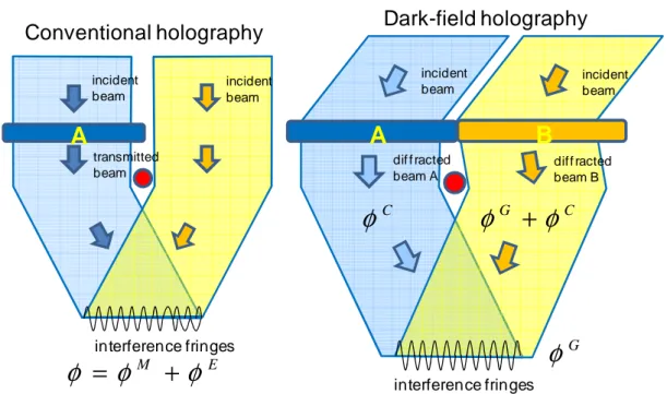
Conventional holography
incident beam incident beam transmitted beam interference fringes dif f racted beam ADark-field holography
incident beam incident beamA
dif f racted beam B interference fringesB
E Mφ
φ
φ
=
+
Cφ
φ
G+
φ
C Gφ
Figure 1. Schematic representation of conventional off-axis holography (left) and
dark-field electron holography (right). Transmitted beam in the vacuum, and diffracted beam from unstrained crystal, serve as references for the former and latter respectively.
The technique has a number of advantages over geometric phase analysis (GPA) of high-resolution images for the study of transistors. The specimens do not need to be as thin, being more like those of conventional TEM. Specimens are therefore easier to prepare and the effects of thin-film relaxation reduced. The major advantage, however, is the ability to analyse large regions of crystal at relatively low resolution.
Results will be presented for two different strained-silicon samples. TEM specimens are prepared by focussed ion beam (FIB) to thicknesses of between 100 and 200 nm. Observations are carried out on the SACTEM-Toulouse, a Tecnai (FEI) 200kV TEM equipped with a Cs corrector (CEOS), rotatable biprism and 2k CCD camera (Gatan). The microscope is operated in a pseudo-Lorentz mode using the corrector first transfer lens as a pseudo-Lorentz lens and with the main objective lens and hexapoles switched off [8]. Results will also be shown with the new aberration-corrected Lorentz mode (CEOS). Typical fringe spacings are 1-2 nm and hologram widths from 300-500 nm allowing lengthwise fields of view of several microns. Strain fields are extracted using a modified version of GPA Phase 2.0 (HREM Research Inc.), a plug-in for DigitalMicrograph (Gatan).
2.Theory
The phase appearing in geometric phase analysis (GPA) is usually presented in the perspective of high-resolution electron microscopy [3]. Here, we need to place it in a wider context: that of the other phases measured in electron microscopy – in particular by electron holography.
The wave function of the fast electron at the exit surface of a non-perfect crystal can be written:
{
gr}
r r) ( )exp 2 . ( i gψg π ψ =∑
(1)Electron Microscopy and Analysis Group Conference 2009 (EMAG 2009) IOP Publishing Journal of Physics: Conference Series 241 (2010) 012027 doi:10.1088/1742-6596/241/1/012027
where r is in the xy-plane, conjugate with the image plane, and the phase term due to the forward momentum is implicit. The local Fourier components have an amplitude and phase:
{
( )}
exp ) ( ) (r g r g r g a iφ
ψ
= (2)corresponding to the complex amplitudes of the diffracted beams as a function of position across the exit surface of the crystal [9]. The phases here refer uniquely to the phases of Fourier components in reciprocal space and not those of the wave function in real space. The phase can be written as having four components:
)
(
)
(
)
(
)
(
)
(
r
r
r
r
gGr
E g M g C g gφ
φ
φ
φ
φ
=
+
+
+
(3)crystalline, magnetic, electrostatic and geometric phase. Crystalline phase is due to the (dynamical) diffraction of the fast electron by the crystalline potential, and electrostatic phase includes contributions from the mean inner potential of the material. We choose explicitly the origin to coincide with an axis of symmetry of the crystal. Geometric phase therefore arises from any local displacement,
u(r), of the crystal with respect to this axis:
φ
gG(
r
)
=
−
2
π
g
.
u
(
r
)
. (4)It is in this context that the setup for dark-field electron holography was imagined [5]. If the diffracted beams can be interfered, the geometric phase component can be measured directly. To measure strain, the requirement is the elimination of the other phase terms, notably crystalline and electric phase. To a first approximation, these two phases do not depend directly on the local strain. Therefore, if the sample is uniformly thick, these terms will constant and will not contribute to the measured strain as this is determined from the gradient of the geometric phase [3]. Nevertheless, where thickness variations are present, the electric phase can be removed, as the example will show.
3.Strained-silicon test sample
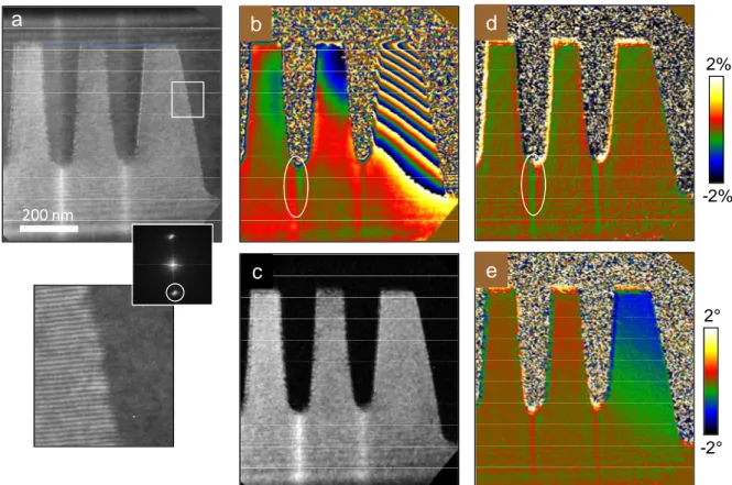
Figure 1 shows a test structure for the study of stress liners. It consists of a comb-like periodical array of etched silicon trenches a few hundred of nanometers deep and about 50-100 wide. The Si is covered by a capping layer of a few tens of nanometers thick of Si3N4 followed by silicon oxide. The differences in thermal expansion coefficients between the different materials results in a high level of stress in the nitride layer after processing, which will in turn deform the silicon.
200 nm
Figure 2. Conventional bright-field image of comb-like Si test structure
for Si3N4 stress liners. Analysed zone (square) and curtaining effect from FIB specimen preparation (oval) indicated.
Electron Microscopy and Analysis Group Conference 2009 (EMAG 2009) IOP Publishing Journal of Physics: Conference Series 241 (2010) 012027 doi:10.1088/1742-6596/241/1/012027
Figure 2 shows the analysis of a dark-field hologram obtained using a (111) diffracted beam. A two-beam condition was chosen to maximise the diffracted intensity and to limit multi-beam dynamical scattering effects. The characteristic feature of a dark-field hologram is that there are no interference fringes in the vacuum (see inset figure 2a), excepting the Fresnel fringes from the biprism. The hologram is analysed as usual by masking the side band in Fourier space to produce the phase (figure 2b) and amplitude maps (figure 2c). The deformation of the (111) lattice planes is determined directly by numerical differentiation of the phase (figures 2d and 2e), as in conventional geometric phase analysis.
The major component of the deformation is in the rotation of the (111) lattice planes in the end-most element of the structure. Artefacts from the specimen preparation can also be seen in the substrate that arise from the local variation in specimen thickness from curtaining during the FIB preparation. High frequency artefacts are also present from the Fresnel fringes. We will show how these artefacts can be corrected for later.
200 nm -2° 2° -2% 2%
a
b
c
e
d
Figure 3. Analysis of dark-field hologram: (a) dark-field hologram from (111) diffracted beam,
Fourier transform and zoom inset; (b) phase; (c) amplitude; (d) local variation in planar spacing; (e) local lattice plane rotation.
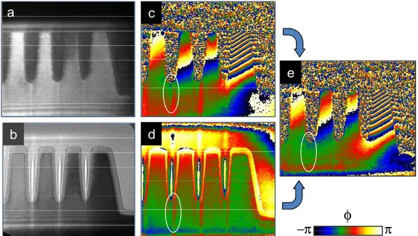
Figure 4 shows the bright-field and dark-field electron holograms from the same area in a repeat experiment. The bright-field hologram was formed by interfering the transmitted beam from the substrate with the transmitted beam from the strained area, in an exact analogy with the dark-field hologram. This hologram should only contain phase changes due to the crystalline phase and the mean inner potential of the surrounding material. Figure 4e shows the result of the subtraction of the dark-field phase (figure 4c) and the bright-dark-field phase (figure 4d). It can be seen that the artefacts due to the thickness variations have been successfully removed. This is confirmed in the rotation maps (figure 5). For this example we have also removed the Fresnel fringe artefacts by Fourier filtering.
Electron Microscopy and Analysis Group Conference 2009 (EMAG 2009) IOP Publishing Journal of Physics: Conference Series 241 (2010) 012027 doi:10.1088/1742-6596/241/1/012027
−π
φ
π
b
d
c
e
a
Figure 4. Correction of thickness artefacts: (a) dark-field electron hologram; (b) bright-field
hologram; (c) dark-field phase; (d) bright-field phase; (e) subtraction of the dark-field and bright-field phases. Ovals indicate principle artefacts. Fresnel fringes have been removed by Fourier filtering.
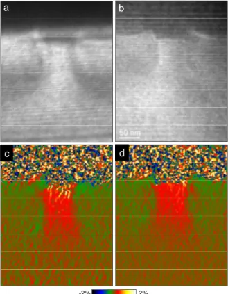
b a
Figure 5. Rotation maps before (a) and after (b) removal of the thickness variation artefacts. The
Fresnel fringe artefacts have also been removed from (b) by Fourier filtering.
4.Aberration-corrected Lorentz mode
The first experiment showed results using the pseudo-Lorentz mode with the hexapoles of the corrector switched off. Figure 6a shows the typical problems we have encountered using this mode. The sample is a strain-silicon n-MOSFET transistor, previously studied in detail using the HoloDark technique [10]. The astigmatism and coma are difficult to correct, particularly in the low-light conditions of dark-field imaging. In addition, the minimum steps in defocus are rather large. Nevertheless, excellent information can be obtained from such holograms and we have measured the strain to a precision of 2.10-4 at 4 nm spatial resolution [10].
Recently, an aberration-corrected Lorentz mode has been designed and installed on our microscope which utilises the hexapoles to correct the aberrations of the first transfer lens. Results for the same sample are shown in figure 6b. The image is much clearer and well defined. The deformation map has a signal-to-noise 60% higher than the previous example, using identical image processing. Whilst better holograms are possible in the non-corrected mode, they are much more difficult to obtain. The corrected mode in particular promises to increase the spatial resolution of the Lorentz mode, and this we will be investigated on suitable test samples in the future.
Electron Microscopy and Analysis Group Conference 2009 (EMAG 2009) IOP Publishing Journal of Physics: Conference Series 241 (2010) 012027 doi:10.1088/1742-6596/241/1/012027
-2% 2%
a b
c d
Figure 6. Comparison of pseudo-Lorentz mode (a,c) and aberration-corrected Lorentz
mode (b,d). Dark-field electron holograms from the (004) beam (a,b) and corresponding deformation maps (c,d).
5.References
[1] Spence J C H and Zuo J M 1992 Electron Microdiffraction (Plenum Press, New York) [2] Houdellier F, Roucau C, Clément L, Rouvière J-L and Casanove M-J 2006 Ultramicroscopy
106 951
[3] Hÿtch M J, Snoeck E and Kilaas R 1998 Ultramicroscopy 74 131
[4] Hüe F, Hÿtch M J, Bender H, Houdellier F and Claverie A 2008 Phys. Rev. Lett. 100 156602 [5] Hÿtch M J, Houdellier F, Hüe F and Snoeck E 2008 Nature 453 1086
[6] Hÿtch M J, Houdellier F, Hüe F and Snoeck E Patent Pending FR N° 07 06711 [7] Hanszen K J 1986 J. Phys. D 19 373
[8] Snoeck E, Hartel P, Müller H, Haider M and Tiemeijer P C 2006 Proc. IMC16 International Microscopy Congress (IMC, Sapporo) vol. 2 p. 730
[9] Hÿtch M J and Plamann T 2001 Ultramicroscopy 87 199
[10] Hüe F, Hÿtch M J, Houdellier F, Claverie A and Bender H 2009 Appl. Phys. Lett. 95 073103
Acknowledgments
The authors thank the European Union for support under the IP3 project ESTEEM (Enabling Science and Technology through European Electron Microscopy, IP3: 0260019), the French Government (MINEFI) through the NANO2012 initiative (project IMASTRAIN), and the French National Agency for Research (ANR) through its program in Nanosciences and Nanotechnologies (HD STRAIN Project No. ANR-08-NANO-0 32). Laurent Clément and Pierre Morin (STMicro, Crolles) are gratefully acknowledged for supplying the stress liner sample. We are indebted to Peter Hartel, Haiko Müller, Stephan Uhlemann and Max Haider (CEOS) for the design and installation of the aberration-corrected Lorentz mode.
Electron Microscopy and Analysis Group Conference 2009 (EMAG 2009) IOP Publishing Journal of Physics: Conference Series 241 (2010) 012027 doi:10.1088/1742-6596/241/1/012027