Charge-Carrier Transport in Amorphous Organic Semiconductors by
Benjie N. Limketkai
Submitted to the Department of Electrical Engineering and Computer Science in partial fulfillment of the requirements for the degree of
Doctor of Philosophy at the
MASSACHUSETTS INSTITUTE OF TECHNOLOGY February 2008
© 2008 Massachusetts Institute of Technology. All rights reserved.
Signature of Author ... ... . --- ... Department of Electrical Engineer and Computer Science
January 11, 2008
C ertified by ...-...
Marc A. Baldo Professor of Electrical Engineering and Computer Science Thesis Supervisor
Accepted by ... .. ... ...
Terry P. Orlando
Professor of Electrical Engineer and Computer Science Chairman, Department Committee on Graduate StudentsARCHIVES
OF TEOHNOLOGYAPR
0 7 2008
LIBRARIES
TABLE OF CONTENTS
Chapter 1 -- Introduction... 7
1.1 Introduction ... ... 7
1.2 Charge-Carrier Transport in Organic Semiconductors ... 8
Chapter 2 - Localization and Transition Rates: From Microscopic to Macroscopic M odels... ... 11
2.1 Introduction ... 11
2.2 Density of States in Disordered Solids ... 11
2.2.1 Localized Band-tail States ... 11
2.2.2 M ott Transition ... ... 12
2.2.3 Anderson Transition ... ... 12
2.3 Localization and Hopping in Organic Semiconductors ... 13
2.3.1 Localization Due to Physical Disorder ... ... 13
2.3.2 Localization Due to Polarization ... ... 14
2.3.3 Hopping Activation Energy... 15
2.4 Polaron Hopping and Marcus Electron Transfer ... 16
2.5 Non-Polaron Hopping Transport in Disordered Solids ... 16
2.5.1 Introduction ... 16
2.5.2 Master Equation of Hopping Kinetics... ... ... 17
2.5.3 Resistor Network Models...18
2.5.4 Variable-Range Hopping (VRH) ... ... 20
2.5.5 Percolation Theory ... ... 21
2.5.6 Transport Energy Level Concept ... ... 26
Chapter 3 - Trapped-Charge-Limited Transport in Organic Semiconductors ... . 29
3.1 Introduction ... 29
3.2 Transport in Organic Molecular Crystals ... ... 30
3.3 Trap-Free Space Charge Limited (SCL) Conduction... 30
3.4 Trapped Charge Limited (TCL) Conduction ... 32
3.4.1 Introduction ... 32
3.4.2 Single Energy Level Trap ... 32
3.4.3 Exponential Distribution of Trap States ... ... 33
3.4.4 Gaussian Distribution of Trap States ... ... 34
Chapter 4 - Bulk-limited Transport in Amorphous Organic Semiconductors ... 35
4.1 Introduction ... 35
4.2 Time-of-Flight Measurement of Charge-Carrier Mobility ... 35
4.3 Temperature and Electric Field Dependences of Mobility ... 36
4.3.1 Introduction ... 36
4.3.2 Mobility Measurements ... 37
4.3.3 'Poole-Frenkel' Electric Field Dependence of Mobility ... 38
4.4 Models to Explain Temperature and Electric Field Dependences of Mobility... 40
4.4.1 The Gaussian Disorder Model (GDM) ... ... 40
4.4.2 The Correlated Disorder Model (CDM)... ... 42
4.4.3 Small Polaron Model ... 44
4.5 Charge-Carrier Density Dependence of Mobility... ... 45
4.7 Model to Explain Combined Temperature, Field, and Density Dependences of
Mobility ... 49
4.8 Doping Dependence of Mobility ... ... 50
4.9 Bulk-limited Current Conduction in Organic Semiconductors using Modified Temperature, Field, Density-Dependent Mobility Expression... 52
4.9.1 Field-Dependent Mobility in SCLC ... 52
4.9.2 Charge-density Dependent Mobility in SCLC ... 53
4.9.3 Field and Charge-density Dependent Mobility in SCLC... 54
Chapter 5 - Percolation Model for Bulk-limited Transport in Amorphous Organic Semiconductors ... 55 5.1 Introduction ... 55 5.2 Theory ... 56 5.2.1 Background... 56 5.2.2 Zero-Field Limit ... 57 5.2.3 Zero-Temperature Limit ... 59
5.2.4 Non-Zero Temperature and Electric Field ... ... 60
5.3 E xperim ent... 61
5.4 C onclusion... 64
5.5 Discussion ... ... 65
Chapter 6 - Injection-limited Transport in Amorphous Organic Semiconductors ... 67
6.1 Introduction... 67
6.2 Modeling Localization and Disorder for Injection... 67
6.3 Interfacial Trap Model for Charge Injection ... ... 70
6.3.1 Introduction ... 70
6.3.2 Metal-Organic Interface ... 71
6.3.3 Interface Roughness and Polarization... 72
6.3.4 Calculation of Current... 76
6.3.5 Current-Voltage Measurements ... ... 78
6.3.6 Discussion... 84
6.3.7 Conclusion... 87
6.4 Injection and/or Bulk Limited Conduction... ... 87
Chapter 7 - Cathode-Doping of Organic Semiconductors ... 89
7.1 Introduction ... 89
7.2 Experimental Results ... 93
7.3 D iscussion... 95
7.3.1 Cathode Metal Forms Interface Traps... ... 95
73.2 Effect of Cathode-doped Charge on J-V Characteristics... 96
7.4 C onclusion ... 99
Chapter 8 - Conclusion ... 100
8.1 Summary and Future Work... 100
Charge-Carrier Transport in Amorphous Organic Semiconductors
by Benjie N. Limketkai
Submitted to the Department of Electrical Engineering and Computer Science on January 11, 2008
in partial fulfillment of the requirements for the degree of Doctor of Philosophy
Abstract
Since the first reports of efficient luminescence and absorption in organic semiconductors, organic light-emitting devices (OLEDs) and photovoltaics (OPVs) have attracted increasing interest. Organic semiconductors have proven to be a promising material set for novel optical and/or electrical devices. Not only do they have the advantage of tunable properties using chemistry, but organic semiconductors hold the potential of being fabricated cheaply with low temperature deposition on flexible plastic substrates, ink jet printing, or roll-to-roll manufacturing. These fabrication techniques are possible because organic semiconductors are composed of molecules weakly held together by van der Waals forces rather than covalent bonds. Van der Waals bonding eliminates the danger of dangling bond traps in amorphous or polycrystalline inorganic films, but results in narrower electronic bandwidths. Combined with spatial and energetic disorder due to weak intermolecular interactions, the small bandwidth leads to localization of charge carriers and electron-hole pairs, called excitons.
Thus, the charge-carrier mobility in organic semiconductors is generally much smaller than in their covalently-bonded, highly-ordered crystalline semiconductor counterparts. Indeed, one major barrier to the use of organic semiconductors is their poor charge transport characteristics. Yet this major component of the operation of disordered organic semiconductor devices remains incompletely understood.
This thesis analyzes charge transport and injection in organic semiconductor materials. A first-principles analytic theory that explains the current-voltage characteristics and charge-carrier mobility for different metal contacts and organic semiconductor materials over a wide range of temperatures, carrier densities, and electric field strengths will be developed. Most significantly, the theory will enable predictive models of organic semiconductor devices based on physical material parameters that may be determined by experimental measurements or quantum chemical simulations. Understanding charge transport and injection through these materials is crucial to enable the rational design for organic device applications, and also contributes to the general knowledge of the physics of materials characterized by charge localization and energetic
disorder.
Thesis Supervisor: Marc A. Baldo Title: Professor of Electrical Engineering
Acknowledgements
First and foremost, I give praise and thanks to the Lord God Almighty, for He is good; His love endures forever. In His great mercy and unfailing love, grace and peace has been given to us through faith in Christ Jesus. This faith is more precious than anything. The Lord is my strength and shield. My heart trusts in Him, and I am helped. My heart leaps for joy, and I am grateful and give thanks to Him forever...
I want to acknowledge my thesis supervisor, Professor Marc Baldo, for his guidance and instruction in conducting scientific research. I thank the Lord, for Marc helped me a lot to better understand the overall process of research and communication. I am thankful to both Marc and Professor Terry Orlando for supporting me in my graduate studies. Aside from being on my thesis committee, Professor Orlando was also my course advisor. He was always very friendly and taught and advised students very well. I want to thank Professor Vladimir Bulovic, who was on my thesis committee, for his motivating enthusiasm in our work and research in the field of organic semiconductors.
I thank Luke Theogarajan for being like a science mentor, who answered all sorts of questions ranging from physics to chemistry to circuits. The Lord blessed him with much knowledge in many different topics. I also want to acknowledge Kaveh Milaninia and Mihai Bora for all the helpful discussions during lunch and our coffee/tea breaks after lunch. Kaveh is a fabrication and experimentalist guru who provided technical advice and help. Mihai is analytic in everything, and so it was always insightful to talk to him, even about random things. And for all their help in various aspects of graduate school and lab work, I'd like to thank everybody else in the Soft Semiconductor group: Kemal Celebi, Mike Currie, Shlomy Goffri, Tim Heidel, Priya Jadhav, Jiye Lee, Jon Mapel, Carlijn Mulder, and Evan Moran. I also want to acknowledge the people in
Professor Bulovic's LOOE (Laboratory of Organic Optoelectronics) group for all their help and for the collaboration between our two groups.
I want to thank Lakshminarayan Srinivasan for all the helpful discussions. And, I am thankful to my wife Lily, my parents, Benito and Thanh-Nhan Lim, and my siblings, Berkeley, Brian, Benson, and Benhan, for all their support in everything.
Chapter 1 - Introduction
1.1 Introduction
Organic semiconductors possess advantages over conventional inorganic semiconductors in certain large area applications, particularly in optoelectronic devices such as displays and solar cells. Yield concerns typically prohibit the fabrication of large area electronics on crystalline inorganic semiconductors. Polycrystalline and amorphous inorganic semiconductors possess defects at boundaries between crystalline grains. Defects degrade the electronic and optical properties and may be sources of instability if there are dangling bonds. In contrast, organic semiconductor devices exhibit good optical properties even when fabricated by low temperature deposition on flexible plastic substrates, ink jet printing, or roll-to-roll manufacturing.' These inexpensive fabrication techniques are possible because of the fundamental nature of the solid-state organic material, which is made up of isolated, individual molecules held together by weak van der Waals bonds. Unlike their inorganic counterparts, molecular solids are atomically ordered - there are no dangling bonds. But the weak intermolecular bonds exacerbate intermolecular disorder that acts to localize electronic states. Importantly, this preserves the optical properties of individual molecules in the solid state.
Electronic devices based on organic semiconductors, such as organic light-emitting diodes (OLED), photovoltaics (OPV), and thin film transistors (OTFT) have attracted considerable interest recently. But perhaps the first commercial use of organic semiconductors was their application as photoconductors on photocopier and laser printer drums. In early photocopiers, amorphous Selenium (a-Se) was used as the photoconductive material. Organic semiconductors were later used because they are non-toxic, inexpensive to coat on the drum, and have an easily controllable spectral response. But it was soon evident that that charge transport in organic semiconductors could not be explained by conventional models. The charge carrier mobility in organic semiconductors varies by orders of magnitude with changes in charge density, electric field or temperature. This realization initiated the field of charge transport in organic semiconductors. In the 1970's, work focused on photoconductive materials such as the
archetype molecularly-doped polymer: a donor-acceptor blend consisting of donor polyvinylcarbazole (PVK) and acceptor trinitrofluorenone (TNF). These disordered molecular-doped polymer films, used for xerography, were the first type of structures used for studying hopping transport in disordered organic systems.2' 3 Although the early studies made significant progress, predictive models of the charge carrier mobility remained a distant goal - a situation that has continued to the present day.
1.2 Charge-Carrier Transport in Organic Semiconductors
Bulk organic semiconductors are macroscopic assemblies of molecules or polymer chains. The constituent molecular components are weakly held together by van der Waals forces. Consequently, they have narrower electronic bandwidths, and their charge carriers and electron-hole pairs, called excitons, are localized to a few molecules. Organic semiconductors are often highly disordered (both spatially and energetically), especially in the amorphous state, and hence, their charge-carrier mobility is smaller than their covalently-bonded, highly-ordered crystalline semiconductor counterparts. Due to the poor mobility, applications for organic semiconductors tend to exploit properties other than electrical conduction, such as strong optical properties and the feasibility of large-area fabrication.
A comparison of van der Waals bonded molecular crystals and covalent atomic crystals is shown in the table below, after Silinsh and Capek.4
Molecular Crystals Covalent Crystals
Weak van der Waals intermolecular Strong covalently bonded interatomic interactions -10-3 - 10-2 eV interactions -2 - 4 eV
Charge-carrier and exciton localization Charge-carrier and exciton delocalization Charge-carrier and exciton energies Single electron approximation determined by many electron interactions
(e.g., polarization)
Charge-carriers and excitons treated as Charge-carriers are free electrons and holes polaronic quasi particles
Low charge-carrier mobility (=u 1 High charge-carrier mobility; long mean cm2/Vs); small mean free path (on the free path (100 - 1000 times lattice
order of lattice constant) at room constant)
temperature
Large effective mass of charge-carriers Small effective mass (less than mass of (100 - 1000 times bigger than electron electron)
mass)
Hopping-type charge transport Frenkel excitons
Low melting and sublimination temperatures; low mechanical strength;
high compressibility;
Table 1-1:4 Comparison of properties of molecular (1994).4
Band-type charge transport Wannier excitons
High melting and sublimination temperatures; high mechanical strength;
low compressibility;
and covalent crystals. After Silinsh and Capek
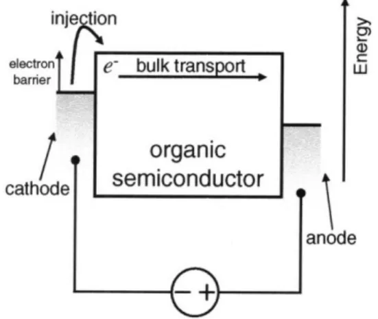
Even though organic semiconductors are typically found in applications that do not require good electronic properties such as high charge carrier mobility, it is important to understand charge transport in organic semiconductors because it typically dominates the behavior of organic semiconductor devices. Models to explain current-voltage characteristics in organic semiconductor devices traditionally assume that conduction is either limited by injection or transport in the bulk.
inje~on,
Figure 1-1: Total current is from the charge injection rate from metal contacts into organic semiconductor and the subsequent bulk transit to the other contact. Most models assume current is dominated by one of these two mechanisms.
Injection-limited models have conventionally been described under a tunneling5' 6
or Richardson-Schottky thermionic emission5 approach. Both models have been
successfully employed for inorganic semiconductors. Tunneling and thermionic emission models have been applied analytically7 and using Monte Carlo simulations8, 9 to describe
injection current in organic semiconductors.
Bulk transport models are based on the drift equation, J = qnaF , where
ft = (n, F, T) . A space-charge limited current (SCLC) model for a perfect insulator with no intrinsic carriers or traps and a constant charge-carrier mobility obeys the Mott-Gurney equation.' One set of bulk-limited models concentrates on the charge-carrier1 density (n) dependence of the charge-carrier mobility. One type of 'n-model' is the trap-charge limited conduction (TCLC) model," which is a modification of the SCLC to include a trap distribution. A charge-density dependence arises because as the charge concentration is increased, the traps fill up to increase the density of available charge in the conduction band that can participate in current motion. A second set of bulk-limited models, the 'F-models', seek to interpret experimental data in terms of an electric-field dependent charge-carrier mobility. Experimental studies of charge transport in organic semiconductors have observed that the electric field dependence of mobility follows an
approximate Poole-Frenkel form, log t-vi .3 Experiments support both models.12
However, it is difficult to explain the temperature, field, and charge density dependence of mobility with a unified theory.
To summarize, charge-carrier transport in organic semiconductors is still not fully understood. A comprehensive explanation for mobility and current-voltage characteristics is needed to optimize general device performance. Not only is a theory for charge transport in organic semiconductors essential to the rational design of these type of devices, it will also help contribute to the general understanding of the physics of materials characterized by charge localization and energetic disorder. This thesis will present a first-principles analytic theory that will give a unified description of the temperature, field, charge density, and material properties dependences of charge transport in solid-state organic semiconductors that can be successfully compared to experiment.
Chapter 2
-
Localization and Transition Rates: From
Microscopic to Macroscopic Models
2.1 Introduction
This chapter begins by defining charge carrier localization and we discuss its causes. Then, we discuss microscopic transition rates for charge-carriers moving within an organic semiconductor material lattice. A macroscopic resistor network13 for current transport is then modeled based on the microscopic behavior.
2.2 Density of States in Disordered Solids
2.2.1 Localized Band-tail States
To describe the density of states in disordered solids, a simple model is used with the following Hamiltonian:14
,
15H =
ZE
j
1)(
+ fijk
)(k
(2.1)
j j,k
where
10)
is the electronic wavefunction at site j, Ej is the energy of site j, and 8, isthe interaction energy between sites j and k. In an ideal crystalline solid, where all the site energies are equal, the Hamiltonian describes a single band with abrupt band edges and bandwidth determined by the interaction energy f .15 In a disordered solid, disorder can be modeled by assigning random site energies from a probability distribution function (assigning random values for the diagonal elements, Ej; hence, the name diagonal disorder). With the inclusion of disorder, the resulting DOS broadens and gains smooth band-tails at the band edges. The band-tail density of states for a d-dimensional
disordered solid will be an exponential, g(E)=Aexp[B(±(E-E)d/2)] , for a probability distribution function, P(Ej)= [(Ej - EA)+(E, -EB)] 14 This
distribution function represents a uniformly random two-component (A,B) alloy
components A and B, respectively. An Anderson disorder model of a uniform probability
distribution function, P(E)
=
-
-E
jwhere W is the width of the distribution
and 0 is a step function, also yields an exponential band-tail.14 This probability
distribution function could represent uniformly varying site energies arising from lattice disorder (structural disorder), where the range of perturbed energies is modeled to be limited by width W. Therefore, an exponential is commonly used to describe the band-tail distribution in disordered materials. Gaussians are also commonly used to represent random disorder.3 Unfortunately, the actual density of states in organic semiconductors is
difficult to measure. Exponential models of the density of states are commonly employed in analytic models, whereas Gaussian densities of states are more common in numerical models. In both cases, however, the width of the distribution is typically a fit parameter, and it is not certain whether the shape of the distribution is significant within the operating range of most organic semiconductor devices. Nevertheless, accurate measurements of the density of states remain an important unsolved problem for organic semiconductors.
2.2.2 Mott Transition
Various types of distribution functions modeling diagonal disorder in solids result in a band with band-tails. For charges in the middle of the band far above the band-tail
states, the effect of disorder will be weak, and their electronic wavefunctions will not decay such that they are localized within a region of space. The states in the middle of the band are extended,14 and the states in the band-tails are localized. Mott16 introduced the
concept of mobility edge, the energy level position that separates the localized states from the extended states. If the Fermi energy is below the mobility edge, the dc conductivity at T = 0 is zero. Once the Fermi energy passes the mobility edge, Mott16 predicted a transition from an insulating to a metallic state (metal-insulator transition).
2.2.3 Anderson Transition
As the disorder is increased, the extended states near the band edge will start to localize and the mobility edges will move further up into the band. Once the disorder is
strong enough such that its width W exceeds the extended states bandwidth, the entire band will be localized. This transition from a metallic to an insulating system by increasing disorder is called an Anderson17 transition. Amorphous organic semiconductors are believed to have large enough disorder that all the states are localized.
2.3 Localization and Hopping in Organic Semiconductors
2.3.1 Localization Due to Physical Disorder
Organic semiconductor films possess various morphologies that all have some degree of disorder, with amorphous films being the most disordered and molecular crystals the most ordered. All organic semiconductors are characterized by weak van der Waals bonding, which gives them weak intermolecular interactions. This weak coupling of molecules results in weak interaction energy f to give narrow electronic bandwidths. For disordered amorphous films, where there is weak conformational, morphological, and molecular order, there will be dispersion in energy levels of the constituent organic molecules. This statistical variation of width W in the energy level distribution of the molecules will overcome the already narrow electronic bands to create Anderson charge localization.17
There are several possible physical causes for the energetic disorder in bulk amorphous films. One source is the random orientation of molecular dipoles in spatially and geometrically disordered molecular films. The energy of a charged molecule in a lattice of polar molecules will be affected by the surrounding dipole interactions. In a physically disordered lattice, the polar molecules are randomly oriented, and charges on different molecule locations will see different surrounding dipole orientations, and consequently have different energies.
Following the work of Young,18 consider a charge sitting on a site in a simple
cubic lattice with lattice spacing ao. The site energies around the charge are located at aon, where n = ii +
jj
+ kk and i, j, and k are the unit lattice vectors. Each lattice point has a probabilityf of having a point dipole p. The energy contributed from the dipole on lattice point n is:1e 4aqp n2 (2.2) 47wa2 n2
The total energy affecting a charge by the surrounding dipoles is E = e, . Assuming
n
that the average energy from the dipole interactions is zero, the variance in energy with isotropic and uncorrelated dipole moments is:'
(E
2)=(ee"n16)=
(e2)=e
P2 2a
n
f
(2.3)The variance in the energetic dipole disorder is then:18
2 1 q2 p2 1 1 q2p2
2=- r f42 f (16.5323) (2.4)
3 1622e a n n 3 16 2s2a4
For Alq3 with a dipole moment of p = 5.3 Debye, the standard deviation of the dipole
disorder is a = 0.13 eV. This disorder width W of 0.13 eV will be sufficient to create localization. The higher order moments make minor corrections but the second order moment is dominant, giving an approximate Gaussian distribution of energy states due to dipole moment disorder.is The higher order moments do affect the tail of the distribution and a simple Gaussian DOS may not be accurate in heavily dipolar amorphous
materials.18-22
2.3.2 Localization Due to Polarization
However, localization does not only occur due to the physical disorder that is present in amorphous films but it can also manifest itself even in well-ordered molecular crystals due to polarization. According to the Born-Oppenheimer approximation, the electronic wavefunction responds instantaneously to changes in nuclear coordinates. Therefore, any nuclear rearrangement due to polarization or temperature must be considered because it affects the electronic wavefunction. The localization time is defined as the length of time a charge resides at a particular site. It is dependent on the physical disorder, average interaction energy t, and other parameters that may influence a charge to hop out of a site, such as the electric field and temperature. Anderson'7 concluded that at zero applied electric field and zero temperature, if the localization condition is satisfied, the charge will remain at the lattice site for infinite time. The different polarization
effects (electronic, molecular, lattice polarization) will influence charge hopping if they occur on times scales shorter than the localization time of the charge.4 The electronic polarization time is significant because the rearrangement of the electronic wavefunctions is relatively instantaneous. The molecular and lattice polarization occurs on much slower time scales and are comparable to localization time of the carriers if the interaction energy f < 0.1 eV.1
The polarization effects can overcome the weak intermolecular energy to distort the molecular lattice. This rearrangement of the surrounding molecules lowers the energy of the charged molecule. The energy required to remove this excess charge will then exceed the nearest neighbor interaction energy, which leads to trapping, or self-localization.4' 23 If these molecular conformation energy changes are a significant contribution to the total activation energy barrier for escape, then not only should the single carrier be considered in a model of charge transport but the surrounding polarized molecules must be considered as well. The motion of the charge and its surrounding polarization is then treated as a quasi-particle known as a polaron.'
2.3.3 Hopping Activation Energy
The effect of localization is that the mean free path of charges is typically of the order of the spacing between adjacent molecular sites, and charges moving through the disordered lattice are scattered at each molecular site.4 The charge transport mechanism is
therefore hopping of charge carriers from one localized state to another within a lattice of molecular sites. Hopping transport is a thermally activated process, where the activation energy, or energy difference of the charge at the initial and final localized state, is determined by two factors. The first is the statistical variation in site energies due to the physical disorder of the organic material, where there is variation in lattice energy contribution to each site because of intermolecular spacing disorder. The second is intramolecular conformational energy changes due to polarization of a charge to the surrounding molecules.3 If localization is dominated by molecular conformational
changes, then charge transfer is thermally activated with an activation energy that is dependent on the active molecular deformations. These models are known as polaron
models. Often, however, energetic disorder is more important in creating localization, and many models only consider static energetic disorder influence on activation energy.
2.4 Polaron Hopping and Marcus Electron Transfer
The charge and its associated polarization cloud are collectively called a polaron, and the properties of this quasi-particle polaron are conserved as the polaron moves through the lattice. The size of the polarization cloud is dependent on the strength of localization and interaction energy. Holstein24' 25 considered the motion of a polaron in a
lattice where the intermolecular overlap between sites is on the order of or less than the activation energy required for a charge to move to another lattice site. This small-polaron model 4-26 is analogous to Marcus theory27, 28 of charge transfer between adjacent donor
and acceptor molecules. Marcus theory deals with the charge transfer mechanism in solution, where reorganization energy comes from the rearrangement of molecular geometry (intramolecular vibration) and polarization of the surrounding molecules in solution (reorientation of dipoles in the solvent) upon addition or removal of an electron to a molecule.27 A parallel can be formed for charge transfer in the solid-state, where the
reorganization energy mainly comes from vibrational relaxation and not rotation of solvent dipoles. Small-polaron models are based on coupling of the charge with low-frequency phonon modes, with a reorganization energy calculated to be twice that of the polaron binding energy.2426
Nuclear rearrangement limits the rate of polaron hopping since from the
Born-Oppenheimer approximation, electronic changes is much faster than molecular rearrangement. Consequently, charge transfer first requires the surrounding molecules to relax to the optimal nuclear arrangement and form an activated complex.
2.5 Non-Polaron Hopping Transport in Disordered Solids
2.5.1 Introduction
Transport in disordered organic semiconductors, and disordered solids in general, is characterized by charge localization and a hopping transport mechanism. Hopping conduction was first applied to describe the anomalous behavior of transport observed in
doped semiconductors at sufficiently low temperatures. One of the first observations was made by Hung and Gliessman29 who measured the Hall coefficient and resistivity of different Germanium samples with different kinds of impurities and concentrations from room temperature down to liquid helium temperatures. According to conventional impurity semiconductor conduction theory, as temperature is reduced, the concentration of the electrons in the conduction band (or holes in the valence band) should decrease, and the resistivity and Hall coefficient should increase. However, Hung and Gliessman29
found that the resistivity saturates and the Hall coefficient reached a maximum at low temperatures. These anomalies led them to conclude that a different mechanism of conduction was taking place at low temperatures.
For low doping concentrations, there is weak overlap and impurity states are localized. At low temperatures, there will be little thermal excitation to the bands and most charges will be localized to the impurity states. In this case, band current becomes negligible, and tunneling conduction of electrons in localized impurity donor states in the gap becomes the predominant process. This phonon-assisted tunneling conduction process was suggested by Mott30 and Conwell.31
2.5.2 Master Equation of Hopping Kinetics
In the regime where the hopping mechanism is predominant, transport is determined by charge-carriers moving from one localized state to another. The hopping motion of charge-carriers can be described by the kinetic master equation:32' 33
= I _ WjiPj (t)(l- P (t)) -WjPW (t)(l- P (t)] (2.5) where iP (t) is the occupational probability of site i at time t and Wij is the transition rate from site i to site j. Often times, under the condition that the system is close to equilibrium, a linearization can be made to the master equation. Several approaches to solve the master equation include the resistor network method,13 percolation theory,34
effective medium theory,35 the continuous-time-random-walk (CTRW) method,36 and the
Green function method.32 Vissenberg presents and discusses these methods used to solve
2.5.3 Resistor Network Models
Miller and Abrahams13 developed a model that reduces the incoherent hopping
transitions in a disordered lattice to a random resistor network. Their13 proposed network
is used to calculate the hopping conductivity G in semiconductors in the presence of a weak external field. In this hopping transport, the electronic states are localized with the wavefunctions decaying like exp [-air - R, ] (a is the inverse localization length, Rj is the spatial position of a site j) and the energy difference between pairs of sites is
AE =IE -EjI>>
,j (8, is interaction energy between sites i and
j;
E
iand E) is the
energy of sites i and j, respectively). A linearization can be applied for weak-field transition rates, IFU - Fji o Gi, (pi - p ) (Gi is related to transition rate Fi from site i to
site j; p, and pi, is the potential at sites i and j, respectively). From detailed balance of rates, the transition rates in the low-field regime is:13
F
ocexp[ -2aIR
1-R,I]exp[-AE/kT],
AE >0 (upwardhops)
(2.6)
(2.6)F,o
exp -2a R -R
1
1,
AE < 0 (downward
hops)
Note that using Miller-Abraham rates assumes that the electron-phonon coupling is weak enough to have polaronic effects be negligible compared to static disorder in the hopping process. The activation energy AE will be only dependent on the site energy differences (caused by static disorder) and not on molecular conformation energies required to form activated complexes for charge transfer.
From the master equation (Eq. (2.5)), the net steady-state current flow from site i to site j is:33
,
37Ii = q WP (1 - Pi ) - W, Pi (1 - P )(2.7)
The occupational probabilities of sites is given by the Fermi-Dirac statistics:
1
P = (2.8)
S1+exp[(E, -u, )/kT]
where yj is the non-equilibrium quasi-electrochemical potential at site i. At equilibrium,
the electrochemical potential is given by ui = - qF -r , where #u is the chemical
non-equilibrium quasi-electrochemical potential deviates from a well-defined equilibrium electrochemical potential as the temperature is reduced, disorder increases, and the applied electric field increases.37 Using Miller-Abrahams hopping rates (Eq. (2.6)), the
net current flow in Eq. (2.7) will be:33, 37
e-2r
Ej-Eil (E(-Ej)/2kT (E•_-,j)/kT E j-Ei)/2kTe(E,-/k e-2 arj e 2kT (e e -e e= qv
(E-/2kT (E-jj)/2kT (-(E)/2k +(E-A)
/2k
-(E-)2kT
+
(E
-)/2kT(2.9)
where the absolute value in the exponential in the numerator comes from the dependence on the energy difference between sites i and j. Eq. (2.9) can be rewritten as:33, 37
exp
[-2ar
]
exp [-IE
-E/2kT sinh[(A
- , )/2kT]I. = qvo (2.10)
2cosh [(E -A,
)/2kT]cosh
(Ej -,
1
)/2kT]
For small deviations from equilibrium (deviations of non-equilibrium quasi-electrochemical potential from equilibrium quasi-electrochemical potential), the net current can be linearized:33, 37
_ qvo
exp
[-2ari
]
exp
[-IEj
-
E1/2kT]
(2.11)
4kT cosh [(E, - )/2kT] cosh [(E, - uj, )/2kT]
where the approximation
sinh
[(,
-, )/2kT]
=
(,
- p,)/2kT
is used. The net current
between the two sites has been linearized to an ohmic current through a resistor with conductance Gij. Therefore, the hopping conduction between sites in a disordered lattice can now be treated with a random resistor network. The disordered hopping conductivity can be found by calculating the conductivity of a random resistor network.
To calculate the conductivity of their network, Miller and Abrahams assumed that the statistical distribution of resistances in the network of localized impurity states only depends on the intersite distances, and not the individual site energies. However, it was later argued that in calculating the total conductivity of their resistor network, the transport paths in their reduced network may not always represent the true paths carrying most of the current.38
Since Miller-Abrahams assumed nearest neighbor hops, the pathway of nearest neighbor hops may reach a site that is isolated far away from any
nearby sites. This difficult path will have little current; and most charges will rather go through a non-nearest neighbor path that is more optimal.
2.5.4 Variable-Range Hopping (VRH)
The assumption of nearest-neighbor hops may be incorrect for low enough temperatures where the thermally-activated hopping rates become much smaller than the spatial tunneling rates. If there is a continuum of localized states, carriers will be able to choose sites with more favorable energies closer to the Fermi level. Mott pointed out that if the activation energy to a nearest neighbor site was large, a more favorable hop might be to a site farther away with a lower activation energy. This tradeoff of energy and distance for the optimal jump depends on the respective transition rates (energy-dependent hops and spatial-(energy-dependent tunneling rates). Since the energy-(energy-dependent transition is thermally-activated, the optimal hopping distance will depend on temperature. This mechanism of hopping conduction is called variable-range hopping
(VRH).39
Mott proposed that variable-range hopping conductivity is determined by optimal hops that maximizes the transition rates over energy and space. Within a sphere of radius R (the average hopping distance), a charge-carrier at the Fermi level will have at least one
available site to hop to that has an energy within an average range, AE :33
4nR3 3
1-= g(EF ) A E AE = (2.12)
3
4xR
'g(E,)
where a uniform density of states is assumed in the vicinity of the Fermi energy, g (E) = g (E,). The conductance can then be written as (using Miller-Abrahams rates):33
G = Go
exp[-2aR-
3
(2.13)
4xR3 g(E,
)kT
(2.13)Maximizing the conductance, the optimal mean hopping distance is:33
R = (2.14)
=
8
akTg
(E,)4This leads to an optimized hopping rate that is proportional to exp [1/T4]. In general, the temperature dependence of the hopping conductivity is:33', 38
U= exp ( (2.15)
where a = 1/(d +1) for a uniform DOS in a d-dimensional system. In general, depending on the DOS and the dimension of the system, the power exponent a in Eq. (2.15) can vary from 0 (hopping dominated by spatial dependent transitions) to 1 (hopping dominated by temperature dependent transitions).33
For, a three-dimensional variable-range hopping system in a uniform DOS (uniform around the Fermi energy), the log of the conductivity should scale as T-V4 . The temperature parameter T1 in Eq. (2.15) is given by:
33'38
Ca3
T = Ca (2.16)
kg(E,)
where C is a dimensionless parameter. The temperature dependence of the conductivity of amorphous germanium from 60K to 300K was found to be consistent with Mott's formula.40-44 Similar temperature dependences were well-described by Mott's formula for amorphous silicon and carbon.42 Mott VRH theory predicts a temperature dependence of conductivity transition from T-V 4 to T- 1/3 with a dimensionality change from 3D to 2D hopping.
2.5.5 Percolation Theory
The Miller-Abrahams network model was independently modified with percolation theory by Ambegaokar et al.,34 Shklovskii and Efros,45 and Pollak.46
Vissenberg and Matters47 later applied percolation theory to successfully describe transport in amorphous organic semiconductor thin-film transistors. Percolation paths are the most optimal paths for current and these paths determine the hopping conductivity of disordered solids. Percolation theory is based on the principle that the disordered hopping conductivity is not determined by the rate of average hops, but it is limited by the rate of the most difficult hops (lowest conductance) in the most conductive path. A review on applications of percolation theory is given by Sahimi.38
In percolation theory, the random resistor network is first viewed as a system made up of individual disconnected clusters, whose average size is dependent on a
reference conductance G. For a given reference conductance G, all conductive pathways between sites with Gi < G are removed from the network, which leaves a collection of spatially disconnected clusters of high conductivity, G, > G. As this threshold reference conductance G is decreased, the size of these isolated clusters increases. The critical percolation conductance is defined as the maximum reference conductance G = G, at the
point when percolation first occurs; meaning, a continuous, infinite cluster (cluster that spans the whole system) first forms. This infinite cluster will be composed of clusters that are all connected by critical conductive links with conductance G,. From percolation theory, the conductivity is limited by these links, and the total conductance of the system is then equal to Gc. To determine the threshold for percolation, the average number of bonds per site is calculated. A bond is defined as a link between two sites which have a conductance Gij > G. As the reference conductance G decreases, the average number of bonds per site B increases. A large average number of bonds per site indicates a large average size of a cluster (collection of sites with Gj > G). Therefore, it is assumed that once the average number of bonds per site B reaches some critical bond number Bc, the average cluster sizes will be large enough such that they all touch and form a continuous pathway that spans the whole disordered system (form an infinte cluster). Vissenberg and Matters47 set the critical bond number to B, = 2.8, which was calculated for a three-dimensional amorphous system.38'48
Assuming near equilibrium and describing the transition rates with Miller-Abrahams hopping rates, from Eq. (2.11), the conductance between sites i and j is given by:33, 37
G = qvo exp [-2arj Iexp
-
Ej - E/2kT4kT cosh [(E - li)/2kT]cosh [(E, - L )/2kT]
where p, and #j are the quasi-electrochemical potentials that deviate from the equilibrium electrochemical potentials, u - qF -r, where u is the chemical potential, F is the applied field, and r is the position of the sites. If the most relevant hops in the critical infinite cluster-binding links involve site energies that are high above the
quasi-electrochemical potential (E - i >> kT ), the conductance in Eq. (2.17) for small applied
electric fields can be approximated in the zero-field limit as:33, 47
G, qkT
EexpEi+Ei
-E-I+ EFeI2kT (2.18)where EF is the Fermi energy (or chemical potential/ ). In this case, the conductance between sites can be written as:33' 47
G=Go exp[-si ] (2.19)
with Go = qvo/kT and:33,
47
s.. = 2ak + (2.20)
2kT
The conductance Gy between sites i and j is now related to sij. At the first formation of an infinite cluster, the clusters (collection of sites with sj < sc) will all bond at the critical
conducting link sc. The conductivity of the disordered system is therefore
T = Co exp[-s] , where sc is the critical exponent of the critical conductance when percolation first occurs (when B = B ).
The average number of bonds B is equal to the density of bonds, Nb, divided by the density of sites that form bonds, Ns, in the material. At the percolation threshold, when B = Bc, the density of bonds is given by:47
Nb = jd3rE
IfdE
ig(Ei) g(Ej)9(s-sij) (2.21)where r11 is integrated in three dimensions over the entire material, g (E) is the DOS in
the material, and 0 is the Heaviside unit step function. The density of sites that form bonds at the percolation threshold (B = B,) is given by:47
N, = dEg(E)0(sckT-IE-E, )
(2.22)
Note that E. = EF + sckT is the maximum energy that participates in bond formation. The maximum energy is obtained in the limit of rj - 0. The maximum distance between sites that can still form bonds is r. = sc/2a (only downward hops occur between
maximally separated bonded sites). Vissenberg and Matters assumed an exponential DOS in their material (amorphous organic semiconductors):47
N
g (E) = kTo
0,
-oo<E<0
E>O
where No is the total density of states (molecular density) per unit volume and To is a characteristic temperature that determines the width of the exponential distribution. They defined a charge-carrier occupation 5, which, for low enough temperatures (T < To) and
charge-carrier concentrations (EF
I
>> kTo), is given by :4 7:8= 1 JdEg(E)f(E, EF)
No (2.24)
where f (E, EF) is the Fermi-Dirac distribution with Fermi energy EF, and F(z)- fdyexp[-yl]y - 1
Substituting Eqs. (2.20) and (2.23) into Eqs. (2.21) and (2.22), Vissenberg and Matters obtained:47
N NJ
7T1N
(
0expLE,
+sckT]
(2.25)where they assumed that most of the hops take place at the tail of the distribution (IE, >> kTo) and that the maximum energy hop forming a bond is large (sekT > kTo). They remarked that their result in Eq. (2.25) is up to a numerical factor in agreement with previous results49-51 that employed different approaches for variable-range hopping (VRH) in an exponential band-tail.
Using Eq. (2.25), the conductivity of the disordered system is given by: -= co0e-' = o 2aT
2aT
rNoS5
STOT
(2.26)Vissenberg and Matters47 noted that their conductivity expression (Eq. (2.26)) has an Arrhenius-like temperature dependence, a oc exp [-EA/kT], with an activation energy EA
(2.23)
-BT (1- TITO) F (1+
TITO)
=exp EFF( T (+
that has a weak (logarithmic) temperature dependence. Recall earlier that the temperature dependence of a general hopping conductivity can be described with:38
r(T) oc exp - (2.27)
Depending on the DOS and the dimension of the system, the power exponent a in Eq. (2.27) can vary from 0 (hopping dominated by spatial dependent transitions) to 1 (hopping dominated by temperature dependent transitions).33
In regards to Eq. (2.27), the temperature dependence (a= 1) is different from Mott's law for 3D VRH in a constant DOS ( a= 1/4). Vissenberg and Matters47
rationalized that for a constant DOS, hopping high in energy or over large distances play an equal role (however, the spatial dependence is slightly more important since a = 1/4 is closer to 0), whereas for an exponential DOS (where there are increasingly more available states at higher energies), the thermally-activated transition plays a stronger role than the spatial-dependent transition (hence, a close to 1). They further pointed out that it has been previously shown that hopping charges in an exponential DOS can be described as charge motion that is dominated by thermal-activation from the Fermi level to a particular transport energy level.52 The Arrhenius activation energy is then simply the
difference between the transport energy level and the Fermi level. Note that for very low temperatures (sckT < kTo), approximations used to obtain Eq. (2.26) are no longer valid. In this regime, charges will mainly hop near the Fermi energy. The conductivity should transition to VRH near the Fermi energy in an approximately constant DOS (small deviation in energy from Fermi level in exponential DOS).
For very low temperatures, the maximum energy of a site forming a bond (Em• = EF + skT) is only a small fluctuation about the Fermi energy EF that is smaller than the width of the exponential DOS (sCkT << kTo). Therefore, most of the
charge-carriers participating in bond formations are at sites with energies near the Fermi energy and the distribution of these energies (DOS) is approximately constant. The expression for the critical bond number (Eq. (2.25)) is generalized:33
Bc =gNTo sinh (2scT/To)+6s•cT/To E
Note that for sckT > kTo, the generalized critical bond number expression (Eq. (2.28))
reduces to Eq. (2.25).3 3 However, for very low temperatures (sckT << kTo), the following
conductivity expression is obtained:33
o = uo
e-Sc =
oo
exp Ir5 (2a))3 TBcF(1T/T
(+T/
(2.29)
xTNo(The low-temperature conductivity expression in Eq. (2.29) obeys Mott's 3D
variable-range hopping law in a constant DOS, - exp -(TI/T) 1/4] (see Eq. (2.15)).33 Mott's
law for 3D VRH in uniform DOS is Eq. (2.15) with a = 1/4 and T, Ca3/kN (C is a dimensionless parameter; N is density of states). However, Vissenberg33 remarks that from Eq. (2.29):33
T 40B " kTF (1- T/IT) F (I + TT) (2.30)
( k
TiNo
Therefore, unlike VRH in a constant DOS (where T, = Ca3/kN ), the region in the exponential DOS approximated as constant N = No (T/kToF (1- T/To )F(1 + T/To)) will
be dependent on temperature and charge-carrier concentration.3 3
2.5.6 Transport Energy Level Concept
To simplify the hopping problem theoretically, the mobility-determining hops are assumed to be the multiple carrier hops around a single critical transport energy level within the distribution of localized states.5 3 The importance of a particular energy level in the carrier hop dynamics was recognized by Grtinewald and Thomas,50 who described an activation energy of conductivity in a-Si with a variable-range hopping (VRH) model in an exponential band tail. Monroe also developed a transport energy level concept for an exponential density of band-tail states.5 2 Baranovskii et al.53 studied this transport energy level and found that it is the important energy level that dominates the steady-state and transient hopping transport phenomena in both equilibrium and non-equilibrium conditions. This transport level is the optimal energy for hops, and most hopping events are within its vicinity.
Carrier hopping between localized states is determined by a spatial-dependent tunneling transition rate and energy-dependent Boltzmann rate (see Eq. (2.6) for Miller-Abraham rates). Charges in the shallow states can easily hop upwards in energy but they also have a large number of neighboring sites where they can hop down in energy as well. In a distribution that decreases rapidly with energy, such as an exponential or Gaussian DOS, as charges move to lower trap states, hopping downwards in energy becomes slower because the number of nearby states that are lower in energy decreases dramatically. At this point, the charges will have to hop to closer sites that are higher in energy. Therefore, charges in deep states will mostly be dominated by thermal excitations to higher energies. As charges move up in energy, the hopping down process starts competing as the number of available states lower in energy increases. Whether thermal excitations or downward hops dominate is governed by the competition between the spatial-dependent and energy-dependent transition rates. The energy level at which the thermal excitation begins to dominate is called the transport energy, Et.52 Above this level,
substantial number of carriers hop downwards (the fastest rate is hops down to states near
E,); and below, most hop upwards (fastest rate is to states near Et). The position of this transport energy level is a function of the density of states (transport energy will be higher for steeper DOS) and the temperature. As temperature is decreased, the energy-dependent Boltzmann transition rates will decrease, and the transport level will move lower in energy. The transport energy is similar to the mobility edge in that charges are thermally activated to this energy level and higher, and the current is mainly carried by charges in the these transport states. Hopping upward and downward events in the vicinity of the transport energy level is similar to a multiple-trapping mechanism where the transport energy is the mobility edge. Experimental observations showing evidence of a disordered hopping mechanism and an existence of well-defined activation energies can be justified with the transport energy level concept. Conduction is either dominated by thermal activation to the band edge or by charge hopping within the band-tail states with a transport energy level.
The transport energy level model was developed considering an exponential band-tail, however, Baranovskii et al.54 showed that a transport energy level also existed for density of localized states of the form, g(E)- exp[-(E/E0)1], with A= 2 and 2= 1/2.
Since a transport energy level existed for both these DOS, it should also exist for any intermediate DOS from A = 2 to 2= 1/2.54 Therefore, amorphous materials containing these types of DOS may be theoretically analyzed with the notion of a transport energy level. Baranovskii and co-workers54-57 used the transport energy level concept to derive
the mobility in a Gaussian DOS representing disordered amorphous organic semiconductors.
Chapter 3
-
Trapped-Charge-Limited Transport in Organic
Semiconductors
3.1 Introduction
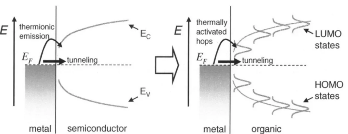
This chapter looks at the macroscopic models for charge transport in relatively ordered organic materials. Models to explain charge transport in organic semiconductor devices traditionally fall into two regimes of operation. One is injection-limited transport which supposes that the injection barrier between the electrode and organic is the main bottleneck for charges to move from one electrode to the other. In this case, the induced current from an applied voltage is rate limited by the properties of the metal/organic interface, i.e. the interface barrier height, interfacial doping, cathode material, interfacial morphology, and etc. The other is a bulk-limited transport model that assumes that the injection barrier is sufficiently low and that the main bottleneck for transport is the organic layer itself. In this case, the charge injection rate across the metal/organic interface is high enough to supply the bulk with an infinite reservoir of carriers. The induced current from an applied voltage is rate limited by the bulk properties of the organic semiconductor, i.e. the trap states in the bulk, the mobility, morphology of organic layer, and etc.
b
0) w
iode
Figure 3-1: Total current is from the charge injection rate from metal contacts into organic semiconductor and the subsequent bulk transit to the other contact. Most models assume current is dominated by one of these two mechanisms.
3.2 Transport in Organic Molecular Crystals
Organic molecular crystals first surfaced as an interest with the evidence of electroluminescence of anthracene crystals.58' 59 Since molecular crystals cannot be easily
grown into thin films, the molecular crystal layers are relatively thick and transport are usually limited by the bulk properties of these materials.
Molecular crystals are ordered van der Waals bonded molecules. Similar to covalent bonded inorganic semiconductors, they may be highly ordered with good electrical properties. But similar to other van der Waals bonded solids, they have relatively narrow bandwidths. Molecular crystals are believed to possess some characteristics of both delocalized band transport and localized hopping.' Since molecular crystals are somewhat well-ordered, the physical disorder should not play a significant role in charge localization. Therefore, if localized charge hopping is believed to operate in organic molecular crystals, the cause should be polaronic effects. When employing band transport models for molecular crystals, the single electron approximation is used; whereas, for more disordered transport, polaron effects that comprises the charge and its associated electronic and molecular polarization clouds are
considered.
The charge-carrier mobility in crystalline naphthalene is observed to increase with decreasing temperature.6 0 This is consistent with band transport because if transport were
from thermally-activated hopping, the mobility would increase with temperature. The temperature dependence of charge carrier mobility follows a power-law behavior, but deviates at higher temperatures, suggesting a transition to polaronic effects.60 Some research has been done in employing a combination of these two types of transports for organic molecular crystals.1
3.3 Trap-Free Space Charge Limited (SCL) Conduction
Organic semiconductors have a relatively low density of free carriers (compared to semiconductors that have narrower bandgaps to allow relatively high density of carriers in the bands at room temperature). In an undoped organic semiconductor, all the charges that carry current must be injected. This charge is uncompensated and gives the organic semiconductor a net charge, known as space charge. Space-charge models for
trap-free insulators, and trapped-charge models with the presence of traps have been applied to describe current in these materials.61-65
One of the most important models for transport in molecular crystals (wide bandgap, insulator crystals) is the space-charge limited current (SCLC) model.10
Assuming that the current is bulk-limited (the injection contact does not limit the current flow into the bulk) and the current density is determined by the drift current for large enough fields and mobility (diffusive process can be neglected; diffusion is usually significant only near the contact):
dn
J = qunF -qD-- = qanF (3.1)
where u is the mobility (v = /F is the drift velocity of the charge-carriers), n the charge density, and F the applied electric field. When a voltage is applied across a material, an electric field is established, causing injected space-charge and thermally-excited charges present in the conduction band to flow from one contact to the other. If current from the injected charge density is comparable to the intrinsic charge density, the semiconductor will no longer be quasi-neutral. For large enough biases, most of the charges contributing to current will be injected space-charge.
A pure molecular crystal will have no intrinsic charges and therefore, the charge density n that contributes to current (in Eq. (3.1)) are all uncompensated charges injected from the contacts. Therefore, the cross-over voltage for pure molecular crystals is very small, and the current-voltage curve is practically all in the space-charge-limited current regime. The electric field from the injected space charge is given from Poisson's equation:
VF = (3.2)
e
where e is the dielectric constant of the molecular crystal. Solving Eqs. (3.1) and (3.2) simultaneously for one dimension and constant mobility, the trap-free space-charge-limited current is obtained (Mott-Gurney law, Child's Law, SCLC square-law):1'0 66
9 V2
JscL =- ep (3.3)
From Eq. (3.3), space-charge limited current gives a slope of 2 on a log Jd- log V plot.
3.4 Trapped Charge Limited (TCL) Conduction
3.4.1 Introduction
For a crystalline semiconductor with no traps in the SCLC regime, the injected space charge will propagate freely with the semiconductor mobility Puo. This is the case for a trap-free solid. However, if there are traps in the bandgap, some of the injected carriers will be lost to these traps and only the fraction of them that remain in the conduction (or valence) band will conduct.64' 65, 67 Since plots of the current-voltage characteristics of organic semiconductor molecular crystals on log-log scales gave slopes much larger than 2,68 it has been proposed that the cause for these high slopes was due to additional trap states that are present in molecular crystals. These trap states will be more predominant in polycrystalline and amorphous molecular solids.
The trap-charged limited current (TCLC) model assumes current is from the motion of drifting carriers trapped and thermally released by localized trap states in the bandgap, and that the frequency of these trapping events is significant enough to limit the conduction. If there is a sufficient density of deep traps, the presence of these traps can have a controlling effect on the mobility. The TCLC modell', 11 65 is a modification of the SCLC model that includes a trap distribution. Note that as higher voltages are applied, the quasi-Fermi level will move closer to the conduction (or valence) band. At the point where the level passes the energy levels of the traps, the traps will be full and all further injected charge will be free. The conduction will then transition to the trap-free limit.65
3.4.2 Single Energy Level Trap
A trap state can originate from an impurity or defect. For single energy level trap
states at ET, with density NT, the density of trapped charges is:'
n, = Ne-(ET-EF)/kT (3.4)
where EF is the quasi Fermi level at an applied bias. The density of charges in the conduction band (or transport energy level) that contribute to the charge motion is:'
no = N ce -(E -E)/kT (3.5)
For current that is dominated by injected charges, the current-voltage characteristics can be described by the equation:'0