HAL Id: tel-02493990
https://tel.archives-ouvertes.fr/tel-02493990v2
Submitted on 28 Feb 2020HAL is a multi-disciplinary open access
archive for the deposit and dissemination of sci-entific research documents, whether they are pub-lished or not. The documents may come from teaching and research institutions in France or abroad, or from public or private research centers.
L’archive ouverte pluridisciplinaire HAL, est destinée au dépôt et à la diffusion de documents scientifiques de niveau recherche, publiés ou non, émanant des établissements d’enseignement et de recherche français ou étrangers, des laboratoires publics ou privés.
Back-gate feedback for auto-calibration of analog and
mixed cells in UTBB-FDSOI technology
Zhaopeng Wei
To cite this version:
Zhaopeng Wei. Back-gate feedback for auto-calibration of analog and mixed cells in UTBB-FDSOI technology. Micro and nanotechnologies/Microelectronics. Université Côte d’Azur, 2019. English. �NNT : 2019AZUR4033�. �tel-02493990v2�
Auto-Polarisation de la Grille Arrière pour
Auto-Calibration de Cellules Analogiques
et Mixtes en Technologie UTBB-FDSOI
Zhaopeng WEI
Polytech’Lab
Présentée en vue de l’obtention du grade de docteur en Electronique d’Université Côte d’Azur
Dirigée par : Gilles Jacquemod Soutenue le : 24 mai 2019
Devant le jury, composé de :
Laurent Fesquet, MCF-HDR, INP Grenoble Pascal Nouet, Professeur, Polytech Montpellier Hervé Barthélémy, Professeur, Université Toulon Yves Leduc, Professeur associé, UNS Nice
Emeric de Foucauld, Ingénieur, CEA-LETI Grenoble Gilles Jacquemod, Professeur, UNS Nice
Université Côte d’Azur – Polytech Nice-Sophia
École Doctorale des Sciences et Technologies de
l’Information et de la Communication
Polytech’Lab
Thèse de doctorat
Présentée en vue de l’obtention du
grade de docteur en Sciences spécialité Electronique
par
Zhaopeng WEI
Auto-Polarisation de la Grille Arrière pour
Auto-Calibration de Cellules Analogiques et
Mixtes en
Technologie UTBB-FDSOI
Thèse dirigée par Gilles JACQUEMOD
Soutenue le 24 Mai 2019
Jury :
L. FESQUET
Rapporteur
MCF-HDR, INP Grenoble
P. NOUET
Rapporteur
Professeur, Polytech Montpellier
G. JACQUEMOD
Directeur
Professeur, UNS Sophia Antipolis
E. de FOUCAULD
Co-Encadrant Ingénieur, CEA-LETI Grenoble
Y. LEDUC
Co-Encadrant
Professeur associé, Polytech Nice-Sophia
Table des Matières
Glossaire ... 1 General introduction ... 3 1. Introduction ... 3 2. Objectives et motivation... 4 3. Thesis work ... 5 4. Bibliography ... 6 Chapter I – FDSOI technology and PLL ... 7 1. Introduction of FDSOI technology ... 7 1.1. End of Moore Law ... 7 1.2. Overview of FDSOI technology ... 10 1.3. Applications of FDSOI technology ... 15 1.4. Conclusion ... 16 2. Phase‐Locked Loop ... 16 2.1. Introduction ... 16 2.2. PLL characteristics ... 18 2.3. PLL applications ... 19 2.4. PLL classifications ... 21 2.5. Conclusion ... 23 3. Jitter and phase noise ... 23 3.1. Introduction ... 23 3.2. Timing jitter definition ... 23 3.3. Phase noise definition ... 26 3.4. Conversion between timing jitter and phase noise... 29 3.5. Conclusion ... 31 4. State of the art for VCO ... 32 5. Conclusion ... 33 6. Bibliography ... 33 Chapter II – Complementary Inverter and Complementary logic ... 37 1. Why to introduce complementary logic? ... 37 1.1. Introduction ... 37 1.2. Differential logic ... 39 1.3. Complementary logic ... 41 2. Complementary inverter in UTBB‐FDSOI ... 43 2.1. Topology of complementary inverter ... 43 2.2. Layout implementation for complementary inverter ... 44 3. Static and dynamic study ... 45 3.1. Sizing strategy ... 45 3.2. Static study ... 48 3.3. Dynamic study ... 52 4. Complementary logic with back‐gate controlled in UTBB‐FDSOI ... 54 5. Conclusion and application examples ... 56 6. Bibliography ... 58Chapter III – Ring oscillators ... 59 1. Presentation of LC and ring oscillators ... 59 1.1. Introduction ... 59 1.2. LC oscillators ... 60 1.3. Ring oscillators ... 62 1.4. Quadrature design ... 66 2. Structure of RO in UTBB‐FDSOI technology ... 68 2.1. Introduction ... 68 2.2. Topology of ring oscillator built with complementary inverters ... 68 2.3. Startup analysis for quadrature ring oscillators ... 70 2.4. Simulation results of four‐complementary RO ... 74 2.5. Comparison of different Vdd ... 76 2.6. Comparison of different sizes ... 79 2.7. Comparison between classic ring oscillator and complementary ring oscillator ... 82 3. Conclusion ... 84 4. Bibliography ... 85 Chapter IV – PLL building blocks ... 87 1. Introduction ... 87 2. Voltage controlled ring oscillator design ... 87 2.1. Introduction of VCO ... 87 2.2. Current mirror with back‐gate control ... 89 2.3. Structure of the VCRO ... 94 2.4. Level shifter ... 94 2.5. Simulation results and discussion ... 97 2.6. Conclusion ... 99 3. Phase detector ... 99 3.1. Introduction of phase detector ... 99 3.2. Introduction of phase‐frequency detector ... 100 3.3. Structure of complementary PFD ... 103 3.4. Simulation results and discussion ... 104 3.5. Conclusion ... 107 4. Charge pump ... 107 4.1. Introduction of charge pump ... 107 4.2. Structure of proposed CP ... 109 4.3. Simulation results and discussion ... 110 4.4. Conclusion ... 114 5. Frequency divider ... 114 5.1. Introduction ... 114 5.2. Introduction of prescaler based divider ... 114 5.3. Proposed LFSR based divider ... 116 5.4. Design of LFSR based divider ... 118 5.5. Simulation and discussion ... 123 5.6. Conclusion ... 126 6. PLL behavioral level simulation ... 127 7. Conclusion ... 129 8. Bibliography ... 130
Chapter V – Test chip and measurements ... 133 1. Introduction ... 133 2. Common‐centroid layout ... 133 3. Layout design ... 136 3.1. Overview of the ROSCOE test chip ... 136 3.2. Layout implementation for each block ... 138 4. Measurements and discussion ... 141 4.1. Measurement test bench ... 141 4.2. Complementary inverter ... 142 4.3. Current mirror ... 143 4.4. Ring oscillator ... 146 4.5. VCRO ... 150 5. Conclusion ... 151 6. Bibliography ... 152 General conclusion and trends ... 153 1. Conclusion ... 153 2. Trends ... 154 Publications liées à cette thèse ... 157 Annex 1: Introductions générale en français ... 159 Annex 2: NAPA code for 15‐bit LFSR ... 163 Annex 2: NAPA code for DPLL ... 165 Résumé‐Abstract ... 167
Glossaire
Pour faciliter la lecture du manuscrit, nous rappelons dans le tableau ci‐dessous les acronymes les plus utilisés. Ils sont également décrits lors de leur première utilisation dans ce mémoire.ADC
Analog to Digital Convertor (or DAC : Digital to Analog Convertor)
ADPLL
All‐Digital PLL
BG
Back‐Gate
BJT
Bipolar Junction Transistor
CDR
Clock and Data Recovery
CP
Charge Pump
DCVSL
Differential Cascode Voltage Switch Logic
DIBL
Drain Induced Barrier Lowering
DPLL
Digital PLL
DVFS
Dynamic Voltage Frequency Scaling
ECL
Emitter‐Coupled Logic
FDSOI
Fully Depleted Silicon On Insulator
GIDL
Gate Induced Drain Lowering
ISF
Impulse Sensitivity Function
LER
Line Edge Roughness
LFSR
Linear‐Feedback Shift Register
LPF
Low‐Pass Filter
LPLL
Analog or Linear PLL
LPT
Linear Phase Time
LTI
Linear Time Invariant
LVT
Low Voltage Transistor (Low V
Th)
PD
Phase Detector
Probability Density Function
PFD
Phase‐Frequency Detector
PLL
Phase‐Locked Loop
PN
Phase Noise
QVCO
Quadrature VCO
RDF
Random Dopant Fluctuations
RMS
Root Mean Square
RO
Ring Oscillator
RVT
Regular Voltage Transistor (Regular V
Th)
TOx
Thickness Oxide
SCE
Short Channel Effect
SNR
Signal to Noise Ratio
UTBB
Ultra‐Thin Buried Box
VCO
Voltage Controlled Oscillator
VCRO
Voltage Controlled Ring Oscillator
V
ThThreshold Voltage
General introduction
1.
Introduction
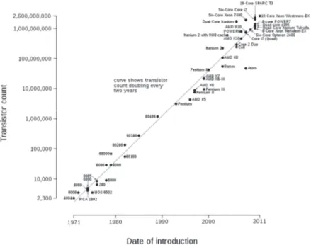
The continuous increase for over 40 years of the performance of microelectronics technology is made possible by miniaturization of elementary components. The prediction of Gordon Moore [1], known as Moore's law (the density of transistors on a chip doubles every 18 months), proved to be uncannily accuracy, partly because the law was the keystone in long term planning in the semiconductor industry for research and development. However, the traditional MOS bulk transistor reaches its limits: short channel effect (SCE) and drain induced barrier lowering (DIBL), lowering of the threshold voltage (Vth) and slowing down of the decrease of the supply voltage Vdd, more power dissipation, less speed gain, less accuracy, variability and reliability issues, ... As shown in Figure 1, this is mainly the result of random fluctuations in the number of doping (RDF: random dopant fluctuations, cf. Figure 1.a) in the channel region, the roughness of the photolithography (LER: Line Edge Roughness, cf. Figure 1.b), and to a lesser extent, among other things, the variation in oxide thickness (TOx: Thickness Oxide, cf. Figure 1.c) [2].
(a) RDF (b) LER (c) TOx Figure 1: Different sources of variability [2]
To overcome these problems induced by the increasingly aggressive technological nodes of 28nm and beyond, two solutions have adopted transistors whose channel is not doped [3] like the FinFET [4] and FDSOI [5] technologies. However, these technologies were initially designed for digital applications, so we can ask whether these transistors are suitable for analog and RF circuits? Moreover, while the digital blocks continue to follow Moore's law (i.e. to decrease area), this is not the case for analogue circuits and especially for passive components (cf. Figure 2) [6]. Decreasing the analogue part and removing the passive components of a complex chip system reduces the total area
of the circuit, or even its consumption. For example, ring oscillators (oscillators without passive elements like inductors and capacitors) are known to present high phase noise, but this design aggressively tackles the size and reduction of energy consumption. We propose, by the possibility of the bias of the back‐gate offered by FDSOI technology, to compensate for variability, short channel effects ... in order to increase the performance of such circuits.
Figure 2: Area reduction problems for analogue components
2.
Objectives et motivation
In the competition of the miniaturization of integrated electronic circuits, it now seems to be assumed that UTBB‐FDSOI (Ultra‐Thin Body and Buried oxide Fully Depleted Silicon on Insulator) technologies are better suited to nanometric sizes. Indeed, they can limit the problems due to random variations of the doping used in conventional transistors of the "bulk" type and make a significant improvement in terms of performance and low power design. The thesis work presented here makes a significant contribution to the development and design of new basic blocks for the design and realization of a phase‐lock loop (PLL) using the logic in 28nm FDSOI technology. Thanks to the latter, we have proposed a complementary inverter based on a pair of inverters with cross‐ coupling of the back‐gates providing output of symmetrical and complementary signals. This concept can be extended to all digital cells to generate more stable, symmetrical and resilient output signals. First we designed an oscillator in fast and efficient rings composed by four complementary inverters delivering quadrature quality clocks with a measured oscillation frequency of 2.3GHz.
Then, using the complementary logic and control of the back‐gate of this technology, we propose an effective solution to design new structures of VRCO, charge pump based on a new
topology of current mirror, PFD, divisor etc., which are the basic elements of high‐speed and low‐ noise PLL. All these designs have been simulated and verified under Cadence. In addition, a test chip composed by complementary inverter, RO, current mirror and VCRO has already been made in silicon and tested, validating all our work.
3.
Thesis work
The present dissertation is composed of 5 chapters, framed by a general introduction and a conclusion including some perspectives for improvement and trends. At the end of the manuscript there are also some annexes, as well as all the publications related to this thesis work.
In the first chapter, we present the limits reached by the classic bulk MOS technology and the announced end of Moore's law. For 22nm technology nodes and beyond, the transistor channel is no longer doped, either for FinFET or UTBB‐FDSOI transistors. The main features of the FDSOI technology are then described as well as these advantages and applications. To illustrate the latter for analogue designs, our choice has been to design a phase‐locked loop (PLL). The operating principle and characteristics of a PLL are given also in this chapter. The focus is on jitter and phase noise, generally low point of ring oscillators (RO). The aim of this thesis is to take advantage of the FDSOI technology to propose a new structure of RO in order to reduce jitter while continuing to limit the consumption and the area of the final circuit.
The second chapter is dedicated to complementary logic. We describe the difference between differential logic and complementary logic, before presenting the implementation of a complementary inverter in FDSOI technology. The innovative structure of such an inverter is based on the crossing of the back‐gates of each inverter to mirror the complementary output signals. The objective of this structure is to limit the switching noise and to offer identical propagation times between the two inverters in order to limit the jitter of a ring oscillator made from these complementary inverters. A static and dynamic study allows to validate this concept and optimize the size of transistors. This concept is then extended to all digital logic gates and an example of a clock generator is proposed.
In the third chapter, we describe the theory of oscillators with a focus on the basic topologies of ring oscillators (RO). We show in particular that the complementary inverters allow to realize quadrature oscillators with a very simple design. A thorough study of this architecture allows to investigate the advantages and limitations. Again, this study also allowed us to optimize the sizing of transistors and to evaluate the performance of the RO, by SPICE simulations.
Chapter four describes all the basic blocks of a PLL, namely the VCRO, the phase detector (PD and PFD), the charge pump and the frequency divider. For each block, basic topologies are described, and then adapted to our concept of complementary logic implemented in FDSOI technology. SPICE simulations allow each time to optimize the size of the transistors and to evaluate the performance of the circuits. A special effort has been made in the design and realization of the new structure of the current mirror which allows to limit the short channel effects while drastically decreasing the size of the transistors. To conclude this chapter, a high‐level simulation, based on the NAPA Simulator, validated the PLL topology build from these basic blocks.
The final chapter is dedicated to the realization of a test circuit in FDSOI technology. We present the realization of the layout design, then the one of the final circuit implementing all the basic blocks in order to test them separately to the VCRO. The entire PLL was not realized. All the measurements carried out are present in this chapter and allow to validate the concept of complementary logic using the crossover of the back‐gates of the UTBB‐FDSOI transistors. The results, in terms of performance, are very promising for the continuation of this work. Finally, general conclusions and some perspectives end this manuscript. Publications related to this thesis work are also presented, followed by a few annexes.
4.
Bibliography
[1] G. Moore, “Cramming more components onto integrated circuits”, Electronics Magazine, Volume 38, n° 8, 1965, http://download.intel.com/museum/Moores_Law/Articles_Press‐ _Releases/Gordon_Moore_1965_Article.pdf
[2] A. Asenov, “Device‐Circuit Interplay in the Simulation of Statistical CMOS Variability”, VARI, Nice, 2012
[3] Khaled Ahmed & Klaus Schuegraf, “Transistor Wars”, IEEE Spectrum, “Rival architectures face off in a bid to Keep Moore’s Law alive”, Nov. 2011
[4] M. Jurczak, N. Collaert, A. Veloso, T. Hoffman & S. Biesemans, “Review of FINFET technology”, SOI Conference, 2009, DOI:10.1109/SOI.2009.5318794
[5] N. Planes et al., “28nm FDSOI technology platform for high‐speed low‐ digital applications”, Digest of technical Papers ‐ Symposium on VLSI Technology, Vol. 33, n° 4, 2012, p. 133‐134 [6] http://download.intel.com/newsroom/kits/idf/2012_fall/pdfs/IDF2012_Justin_Rattner.pdf
Chapter I – FDSOI technology and PLL
1.
Introduction of FDSOI technology
1.1.
End of Moore Law
In 1958, Jack Kilby from Texas Instruments invented the first integrated circuit (IC) composed of a simple flip‐flop with two bipolar transistors on a single chip of germanium, thereby initiating the “Silicon Age”. Early ICs used bipolar junction transistors which suffer from more static power dissipation problems. In 1959, the first metal–oxide–semiconductor field‐effect (MOSFET) transistor was realized by Kahng Dawon from Bell Labs. Because of its low power, reliable performance and high speed, CMOS technology composed by MOS transistors replaced bipolar technology for all digital applications and plenty of analog applications. Both IC and MOSFET create together a grand “micro world” (cf. Figure 1.1).
Figure 1.1: The first integrated circuit by Jack Kilby and the first MOSFET by Kahng Dawon [1] [2]
In the past few decades, the integrated circuits and the semiconductor industries have been experienced a rapid development. The size of transistors is getting smaller and smaller, the degree of IC integration is getting higher and higher and the number of integrated circuits has increased rapidly. From the beginning a transistor has a big size of centimeters until now a fingernail‐sized CPU integrates more than billions of transistors. The size scaling and CMOS process technology improvements continue to increase circuit speeds. Moreover, with the help of chip packaging technology, the price/performance ratio of CMOS‐based microelectronics products is further improved.
Gordon Moore predicted in 1965, known as Moore’s Law: the complexity for minimum component costs has increased at a rate of roughly a factor of two per year [3]. After corrected that the density of transistors on a chip doubles every 18 months by Intel executive David House, Moore’s Law has proven to be uncannily accurate according to the statistics of International Technology Roadmap for Semiconductor (ITRS) (cf. Figure 1.2). Moore's Law has always been an important leading target for semiconductor industry research and development planning.
Figure 1.2: Moore's law and number of transistors in Intel microprocessors
However, in recent years the development of integrated circuits is likely to be not kept up with the trend of Moore's Law. The traditional bulk MOS transistor cannot continue to shrink below 32nm technology node due to various limitations encountered: Sub‐threshold Slope (SS), Short Channel Effect (SCE), Drain Induced Barrier Lowering (DIBL) (cf. Figure 1.3), Threshold Voltage (VTh) and Vdd scaling slowing down, more power dissipation, less speed gain, less accuracy, variability and reliability issues.
Moreover, random dopant fluctuation problem is a big challenge for traditional bulk MOS transistors because they should rely on doping n+ electrons or p+ holes to improve the electronic characteristics. However, channel doping based on random distribution of small concentration of dopants is an inevitable hit by the technology scaling of bulk MOS Transistor. As show in Figure 1.4, as the size is scaled to tens of nanometers, the number of dopant atoms is few even can be counted on finger. In fact, the channel region has only about 50 atoms of dopants at 22 nm node.
Figure 1.4: Atoms dopants and atoms Si scaling
We expect a lot of variability between adjacent transistors on the same die and the dopant variation will cause directly a threshold voltage mismatch between adjacent transistors (VTh variability). Other materials may be taken as the base to reduce the introduction of doping. But one of the main points is the manufacturability, which can be summarized by the ability to create profitable IC’s. Up to now, the industrial solutions are focus on silicon CMOS technology.
We can notice from Figure 1.4 that as the channel size scales, the Si atom still has a large amount. So, undoped channel transistor is a good solution for 28 nm node and beyond. FinFET and UTBB‐FDSOI technology are two silicon technologies which have undoped transistors and only rely on work functions of the metal gate electrode.
Fin Field‐effect transistor (FinFET) [4] is a MOSFET built on a substrate where gate controls a thin body from more than one side of the channel, forming a double gate structure as shown in Figure 1.5. Different from conventional bulk MOS transistor, the gate structure in FinFET is wrapped around the channel and the body is thin, providing better SCEs, it means that FinFET suffers less from dopant‐induced variations. In bulk MOS transistor, the channel is horizontal; while it is vertical in FinFET. So for FinFET, the height of the channel (Fin) determines the width of the transistor. The total width of the channel is given by Equation 1.1: Width of Channel = 2 X Fin Height + Fin Width (1.1) FinFET technology provides higher drive current for a given transistor footprint, hence lower gate delay, lower leakage, no random dopant fluctuation, hence better mobility and scaling of the transistor beyond 28nm. FinFET chips have already utilized in today’s commercial chips at 22 nm and below for digital applications.
Nonetheless, FinFET technology suffers from complex manufacturing process, and its supply voltage is difficult to shrink below 0.7 V. So, it is not suitable for flexible analog circuit design.
UTBB‐FDSOI technology is a good choice for analog & RF design, especially for low power applications, which we will introduce in the next section.
1.2.
Overview of FDSOI technology
Contrary to FinFET technology, Fully Depleted Silicon on Insulator (FDSOI) technology is a planar process technology that delivers the benefits of reduced silicon geometries while containing the complexity of the manufacturing process. Compared to classical bulk MOS transistor technology, FDSOI technology brings a significant improvement in terms of performance and low power design at 28nm node and beyond [6]. Its strength comes from two major innovations as shown in Figure 1.6.
First, an ultra‐thin layer of insulator about 25 nm, called the buried oxide (BOx), is positioned on top of the base silicon. Secondly, a very thin silicon film about 7 nm implements the transistor channel. Thanks to its thinness, there is no need to dope the channel, thus making the transistor fully depleted. The combination of these two innovations is called “ultra‐thin body and buried oxide fully depleted SOI” or UTBB‐FDSOI [7].
As shown in Figure 1.7, the buried oxide separates the conductive channel and substrate. There is no current leakage from channel to substrate which greatly reducing the leakages. Thin Si‐
film helps to improve the electrostatic control, resulting in high speed at low voltage. Moreover, the body being fully depleted, the random dopant fluctuation that plagues bulk CMOS is reduced which helps to lower minimum usable supply voltage.
Figure 1.6: Electron micrograph for ultra-thin body and buried oxide
Figure 1.7: From Bulk-MOS Transistor to UTBB-FDSOI transistor (Source: ST.com)
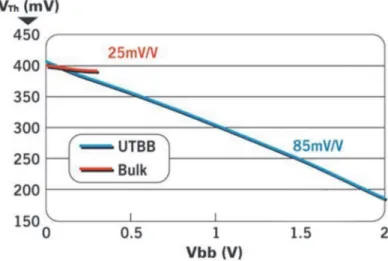
Power/performance claims of 30% to 40%, versus classical Bulk, are not uncommon and FDSOI is already in production at 28 nm and is positioned as an alternate option to bulk 20nm. FDSOI transistors correspond to a simple evolution from conventional MOS transistor. One of the main features of this technology is the possibility to vary the threshold voltage (VTh), using the back‐gate structure of UTBB‐FDSOI transistors. Figure 1.8 presents the back‐gate contact and Figure 1.9 gives the influence of the back‐gate biasing on the VTh variation[8]. It shows that we have more possibility to control VTh in UTBB‐FDSOI technology.
Concern on the process variation on aggressive mode for FDSOI: As the technology scales
down into deca‐nanometer range the variation of the threshold voltage (VTh) becomes an ever‐larger problem. These phenomena are captured by the Pelgrom coefficient (AVT) [9][10] used to define the VTh variation for each transistor. The standard deviation of the VTh variation is given by relation 1. As
shown in Figure 1.10 [11], the AVT for 32 nm bulk CMOS is over 2.5‐3.5 mV.μm. For UTBB‐FDSOI transistors, the AVT is at 1.1 mV.μm and 1.25 mV.μm for 32 nm and 22 nm nodes respectively, mostly due to an undoped channel and hence a significantly limited influence of RDF [12].
Figure 1.8: Back gate biasing possibility [7] Figure 1.9: VTh variation versus BG biasing [7]
Figure 1.10: Pelgrom coefficient versus gate length [11]
The standard deviation on the threshold voltage due to the process variations between a standard CMOS bulk technology and a FDSOI technology is given by the following equations (Equation 1.2 to 1.4).
√ √ (1.2)
∝ . 1 18
1 16 (1.3)
Concern on UTBB FDSOI Transistors: Since UTBB‐FDSOI transistors use undoped silicon films
for the channel, the implant techniques from classical bulk CMOS technology are not relevant. However, the threshold voltage planar UTBB‐FDSOI transistors could be set using other methods such as controlling the gate stack work function, trimming the gate length, counter‐doping, body‐well doping and other methods. The official starting offer of the STMicroelectronics UTBB 28 nm FDSOI technology consists of NMOS and PMOS transistors with two types of threshold voltage, VTh: Regular VTh (RVT) mode for low‐power (LP) applications, as shown in Figure 1.11 and low VTh (LVT) mode for high‐performance (HP) applications, as shown in Figure 1.12.
Figure 1.11: Conventional well architecture in UTBB-FDSOI for LP RVT transistors [13]
Figure 1.12: Flip-well architecture in UTBB-FDSOI for HP LVT transistors [13]
The RVT transistors keep the same layout of a planar bulk CMOS, an n‐well underneath PMOS and a p‐well underneath the NMOS. The lower VTh needed for high‐performance designs is achieved by exchanging places of an n‐well and a p‐well, making PMOS laying in a p‐well and NMOS in an n‐ well. Because of the chosen well‐schedule, the RVT transistors allow full reverse body biasing (RBB) with only slight forward body bias (FBB) capabilities, while it is opposite for the LVT transistors: full FBB up to 3V or more is possible to apply but only limited amount of 300mV of RBB. The LVT type is often referred as a flip‐well and its chosen well‐schedule made available one more functionality called dynamic threshold MOS (DTMOS). This means that gate and back‐gate of the transistor can be bind together and when the gate is turned ON the threshold voltage is reduced with FBB providing minimal on‐resistance per area. FBB mode provides an extremely powerful technique to optimize performance and power consumption. Easy to implement, FBB can be modulated dynamically during the transistor operation, bringing a great flexibility for designers and
letting them design their circuits to be faster when required and more energy efficient when performance isn’t as critical.
It is noticed that in bulk technology the body bias range is limited to ‐300mV in the RBB case due to gate‐induced drain lowering (GIDL) constraints, and to +300mV in the FBB case due to the source‐to‐drain leakage at the junctions as well as the increased risk of latch‐up at high voltage and temperature. Contrarily, the body bias range spans from ‐3V for the RBB case up to 3V for the FBB case in UTBB FDSOI technology, as shown in Figure 1.13. This is mainly aided by the total dielectric isolation of the source and drain provided by the BOX.
Figure 1.13: UTBB-FDSOI flip-well transistor (Triple well) vs bulk body biasing structure
UTBB‐FDSOI technology has proven to be a suitable role in analog and RF design. Figure 1.14 illustrates some advantages of this technology, especially for analog design.
Figure 1.14: Advantages of FDSOI technology for analog design
While the digital blocks continue to shrink, analog one hardly shrinks at all. For example, ring oscillators (digital oscillators without passive elements) are known to exhibit high phase noise, but this design is attractive as it will address aggressively the size (only inverters) and power consumption reduction.
Indeed, we will use the unique back‐gate control structure offered by UTBB‐FDSOI transistors to compensate the mismatches between the different inverters of the ring oscillator to decrease jitter and phase noise.
1.3.
Applications of FDSOI technology
Because UTBB‐FDSOI technology has such excellent performances above, it has a wide range of applications as follows [13]:
1 ‐ Infrastructure Networking: The network infrastructure products benefit from UTBB‐FDSOI to adapt performance and power to workload thanks to FBB. FDSOI provides not only more performance at same voltage than bulk, but also much lower performance degradation when lowering the supply voltage. As a result, it will have a good efficiency on multiprocessing applications. 2 ‐ Consumer devices: UTBB‐FDSOI technology can help optimized SoC integration in Mixed‐ signal and RF applications. Circuits in UTBB‐FDSOI technology show a wide dynamic voltage and frequency scaling (DVFS), extend performances and reduce the power consumption using back‐gate control. For example, a 3GHz dual‐core ARM Cortex TM‐A9 (A9) manufactured in the 28nm UTBB FD‐ SOI technology, compared with equivalent 28 nm bulk CMOS chip, shows an improvement of +240% at 0.6V or +540% at 0.61V with 1.3V FBB [14].
3 ‐ Automotive: UTBB‐FDSOI features low power consumption, fast speed, low cost, etc. It is suitable for use in automotive cameras, processors and radars. It also manages leakages in high temperature environment and guarantees high reliability thanks to highly‐efficient memories.
4 ‐ Internet of things (IoT): The Internet of Things is an environment where each object is provided with unique identifiers and the ability to transfer data over a network without requiring human‐to‐human or human‐to‐computer interaction as shown in Figure 1.15. LoT of embedded objects become more and more popular in our daily lives.
But IoT is not “green”, because every terminal needs energy. The number of connected devices has increased exponentially in recent years as shown in Figure 1.16. With the back‐gate control, UTBB‐FDSOI technology can offer an ultra‐low voltage operation in each device. It can balance power, performance and cost, so FDSOI is a good choice for IoT chips that have special power and cost requirements.
Figure 1.16: IoT terminal development trend (Source: Disruptionhub.com)
1.4.
Conclusion
In this section, we first reviewed the development of the integrated circuit industry and the trend of transistor scaling. With the development of Moore's Law, FinFET technology and UTBB‐ FDSOI technology help Moore's continuation. FinFET is suitable for today’s digital IC applications while UTBB‐FDSOI technology, thanks to its specific back‐gate structure, provides low‐power and more flexible multi‐Vth design for analog and RF applications. Then we introduced the possible applications for UTBB‐FDSOI. What we are very interested in is the application of IoT. We will design novel structure of oscillators and phase‐locked loops in UTBB‐FDSOI technology for low‐power applications. PLL is a very interesting circuit to evaluate this technology for analog, RF and mixed‐ signal design.
2.
Phase‐Locked Loop
2.1.
Introduction
Clock signals are widely used in a variety of circuits. For digital circuits, whether it is synchronous timing or non‐synchronous timing, the correct operation of digital information processing, including calculation, transmission and storage, requires a stable clock. In radio frequency communication, wireless signals are transmitted strictly according to a specific frequency.
Therefore, in RF receiving and transmitting systems, a clock generation circuit called frequency synthesizer is required to generate an accurate clock signal. Also, in wired communication systems, such as in fiber‐optic communications, and in communication systems using metal wires as carriers, digital signals are also modulated to a certain frequency. Accurate clock generation and recovery circuits are a very important part of such systems. A Phase‐Locked Loop (PLL) is such circuit that satisfied all the above functions.
A phase‐locked loop (PLL) is a control system that generates an output signal whose phase is related to the phase of an input signal. More precisely, a PLL is a circuit synchronizing an output signal which is generated by an oscillator with a reference signal in frequency as well as in phase [15]. In the synchronized, often called locked state, the phase error between the output signal and the reference signal is zero, or very small. As a result, a PLL can track the input frequency, or it can generate a frequency that is a multiple (in fact a fractional number) of the input frequency.
The classic PLL topology usually consists in four following blocks:
‐ Phase Frequency Detector (PFD) or Phase Detector (PD): compares the frequency of the input reference signal (from the frequency stable crystal oscillator) and the feedback signal, and outputs a signal representing the difference between the two signals.
‐ Loop filter (LF) or low‐pass filter (LPF): Filters the high‐frequency components of the signal generated from PD, keeping the DC part signal.
‐ Voltage Controlled Oscillator (VCO): Outputs a periodic signal of the corresponding frequency according to the input voltage.
‐ Feedback Loop: usually implemented by a divider, reduces the frequency of the VCO to be compared with the reference signal to compare in PD.
Here we take the RF clock generation circuit as an example to describe the basic operating principle of the PLL circuit. First, a high‐quality reference clock source is used in the clock generation circuit, usually achieved with a quartz oscillator. The frequency of a quartz oscillator cannot be adjusted outside a very limited range around its fundamental frequency or harmonics and produces usually only a fixed clock frequency. So a PLL is required to generate the various desired frequencies. For example in quad‐band GSM RF transmitter, the clock reference source may work at 26 MHz, a PLL is required to generate two distinct signal paths one for low frequency bands (824 to 915MHz) and one for high frequency bands (1710 to 1980MHz) [16].
As shown in Figure 1.17, the PLL is a negative feedback system. In the feedback loop, the output of the VCO is divided by the frequency divider to the low frequency (fVCO/N), and the phase
difference signal is generated comparing with the reference clock in PD. Then the phase difference signal is processed by loop filter in the forward channel generating a voltage signal to control the VCO. As a result, the output clock of the VCO at the back end of the loop is locked at N times the reference clock frequency.
Figure 1.17: PLL block diagram for clock generator application
2.2.
PLL characteristics
The PLL has the following basic characteristics during normal operation: 1) Good narrow band characteristics: When the PLL is in the locked state, the error voltage output from the PD is a DC voltage that can smoothly pass through the loop filter. If there is an interference component in the input signal at this time, the error voltage formed by the interference signal and the output signal of the VCO in the phase detector PD is suppressed by the loop filter (outside the passband of the LPF). Therefore, the interference component in the output signal of the VCO is greatly reduced. The loop of PLL is equivalent to a high‐frequency narrow‐band filter to filter out noise. This narrow‐band filtering characteristic is difficult to achieve with LC, RC, quartz crystal and other filters.2) No frequency difference in locked state
When the PLL is in the locked state, the output signal of the loop is equal to the frequency of the input signal, there is no residual frequency difference, only the remaining phase difference. It achieves better frequency control than the conventional AFC system, and thus has been widely used in automatic frequency control, frequency combining and other applications.
3) Automatic tracking feature
When the frequency of the input signal changes slightly in a locked loop, the frequency of the VCO changes rapidly, making the output frequency close to the input frequency and eventually equal. Even if the loop does not immediately reach the locked state, it can capture the input signal and finally enter the locked state through its own adjustment.
4) Easy to integrate
The building blocks of PLL should be easy to use in integrated circuits. With the development of integration technology, the entire loop, including some amplifying components, control components, etc., can be integrated on a single chip. The circuit integration can reduce chip’s size, save costs, improve reliability and stability, and greatly improve the overall performance.
2.3.
PLL applications
Because of its outstanding performances above, PLLs are widely used in signal filtering, modulation and demodulation of analog and digital signals, frequency multiplication or division, mixing, frequency synthesis etc. We will show some examples to explain the classic applications of PLL as follows:
1) Frequency multiplication, division and mixing
In the basic PLL circuit, if we add a frequency divider, a frequency multiplier or a mixer in the feedback loop, the output frequency of the VCO will be locked at the required frequency, thus achieving frequency multiplication, frequency division or frequency mixing functions respectively.
2) Clock generation
Many microelectronic systems, including processors, operate at hundreds of MHz or GHz frequency. Generally, the clocks supplied to these systems are made with PLL, which multiplies a lower frequency reference clock (usually 50 or 100 MHz) up to the operating frequency of these systems [17].
3) Demodulation of Frequency modulation (FM)
If a PLL is locked to a FM signal, the VCO tracks the instantaneous frequency of the input signal. The filtered error voltage which controls the VCO and maintains lock with the input signal is demodulated FM output. The VCO transfer characteristics determine the linearity of the demodulated out. If the VCO used in the PLL is highly linear, it is possible to realize highly linear FM demodulators.
4) Phase‐locked receiver
The phase‐locked receiver is a narrow‐band tracking PLL with a mixer and intermediate frequency (IF) amplifier at the feedback loop as shown in Figure 1.18 [18]. This receiver is suitable for long‐distance transmission, such as in space technology applications. When the ground receiving station receives the radio signal from satellites, the signal received is extremely weak because of the long distance, small transmitting power and low gain in
antenna. Moreover, because of the Doppler effect, the frequency of the signal received will deviate from the frequency of the signal transmitted by the satellite, and its value tends to vary over a wide range. For such weak signals whose center frequency varies over a wide range, if a conventional receiver such as a superheterodyne receiver is used, the frequency band of the intermediate frequency (IF) amplifier should have a large bandwidth, so that the output signal‐to‐noise ratio (SNR) of the receiver will be seriously degraded. It will not be able to effectively detect the signal. If a phase‐locked receiver is used, which has the narrow‐ band tracking characteristic, the output SNR can be effectively improved, and we can obtain a satisfying receiving effect.
Figure 1.18: Block diagram of PLL receiver
5) Frequency synthesis
RF frequency synthesizer is one of the most important applications for PLLs, which can be found in every communication integrated circuit. As shown in Figure 1.19, the RF receiver & transmitter usually have three main functional subsystems: receiver, transmitter and frequency synthesizer. The function of the frequency synthesizer is to generate the required local oscillation signal for the mixer to receive and transmit at the required frequency. As the PLL can convert the stable and accurate reference frequencies which are provided by crystal oscillators to the specified frequency, it is the ideal module for frequency synthesizers to generate local oscillation signals. The precision of the frequency synthesizer determines the stability and the accuracy of the whole system. As signals are transmitted in specific frequencies in modern communication systems, frequency synthesizers are indispensable components in such systems (cf. Figure 1.19).
Moreover, PLL circuits are also widely used but not limited in clock and data recovery (CDR) [19] [20], jitter and noise reduction, and FSK Frequency‐Hopped Communications [21].
Figure 1.19: Block diagram of RF transceiver
2.4.
PLL classifications
According to the degree of digitization of the building blocks of the PLL, there are 3 types of PLL possible on the hardware level: Linear PLL, digital PLL and all‐digital PLL. Figure 1.20 illustrates the block diagram of a linear PLL (LPLL) which is also the structure of the early PLLs. In LPLLs, the four‐quadrant analog multiplier is used as a PD. The loop filter is built from a passive or active analog RC filter and the well‐known VCO is used to generate the output signals of the LPLL. In most cases the input signal is a sine wave with angular frequency, and the output signal is a symmetrical square wave with angular frequency [15]. In a word, all building blocks in LPLL are based on analog devices and only process analog signals: frequency, phase, or analog voltage etc.Figure 1.20: Block diagram of the Linear PLL (LPLL)
The PLL gradually evolved into digital territory. If a digital PD (EXOR gate, J‐K flip‐flop or phase frequency detector) is used and all other blocks remain the same (analog filter and VCO), this system is called the digital PLL (DPLL) as shown in Figure 1.21. In many DPLL applications such as frequency synthesizer, a divide by N counter is added in the feedback loop as the frequency divider, so the VCO generates a high frequency which is N times the frequency of reference signal.
The DPLLs are used for digital signal processing, but the DPLL performs similarly to the LPLL. The error signal from PD is a binary signal which carries analog information (duty cycle) that modulates the after blocks. The noise of DPLL is better than LPLL because the phase detector is only sensitive to rising edge or falling edge of the compared signals (reference and feedback).
Figure 1.21: Block diagram of the Digital PLL (DPLL)
If the PLL is completely implemented only by digital blocks, without any passive components or linear components, it is called an all‐digital PLL (ADPLL). The block diagram of ADPLL is shown in Figure 1.22. From the figure we can see that the analog loop filter is replaced by a much smaller digital loop filter which allows more flexibility than an analog filter, such as a polyphase or adaptive filter [22]. The VCO is renamed by DCO (Digitally Controlled Oscillator) controlled by digital clock. The signals processed by ADPLL are all digital (binary) and may be a single digital signal or a combination of parallel digital signals.
Figure 1.22: Block diagram of the All-Digital PLL (ADPLL)
Compared to traditional LPLLs and DPLLs, ADPLLs have the advantage of no off‐chip components. ADPLLs are insensitive to technology but at the cost of performance [23]. Moreover, the loop bandwidth and center frequency are programmable and the ADPLL systems do not require A/D (Analog to Digital or D/A: Digital to Analog) conversion when used in digital systems.
Those are three classic PLL structures based on the hardware level. In fact, with the development of today’s PLL technology, PLLs can also be implemented in the software domain. The function of this type of PLL is executed by software and runs on the DSP which is called software PLL (SPLL) [24]. Compared with hardware based PLL, the SPLL is free from complicated hardware circuit design, simple and convenient to modify parameters, has good scalability and anti‐interference ability, and can achieve good speed and good precision at the cost of a higher power consumption. The performance of the SPLL is based on a high‐performance microprocessor or DSP, but in area limited integrated circuits, traditional LPLL and DPLL are still indispensable.
In the actual PLL applications, we should make a careful trade‐off according to performances, price, area, power consumption … to choose appropriate type of PLLs.
2.5.
Conclusion
In this section, we studied the basic components and working principle of the PLL circuits. The working characteristics and application of PLL circuits are given. According to the degree of digitization of the building blocks, we also introduced the different type of PLLs. Our target is to build a very low power PLL using a novel structure for VCO, and then all the building blocks of DPLL in UTBB‐FDSOI technology.
3.
Jitter and phase noise
3.1.
Introduction
In today’s high‐speed communication systems especially in PLL circuits for critical timing applications in systems, it is important to accurately characterize and quantify their noise to determine system performance and reliability [25]. Jitter and phase noise are the major concerns. The former is the performance measurement of noise in the time domain, while the latter is the performance measurement of noise in the frequency domain.
3.2.
Timing jitter definition
In application using clock recovery and clock generators, the clock jitter is a very important feature [26]. General speaking, time jitter means the uncertainty of the clock cycle. In another word, jitter is the deviation from true periodicity of a presumably periodic signal as shown in Figure 1.23.
Figure 1.23: Definition of timing jitter
For clock jitter, there are three commonly used metrics:
Absolute jitter or edge‐to‐edge jitter is a concept of uncertainty that measures the point in time. Absolute jitter represents the time interval error between the real clock edge position measured and the ideal position referenced by an ideal clock. The uncertainty of the time point caused by absolute jitter will affect many sampling circuits. For example, in the clock data recovery circuit (CDR), it is necessary to use the clock edge to sample the center of the data and the edge of the data change. The absolute jitter of the sampling clock has a direct impact on the jitter tolerance of the CDR [27].
Period jitter or cycle jitter is a concept of uncertainty that measures time period and is defined as the periodic deviation between the actual clock period and the ideal or average clock period. Period jitter is important in synchronous circuit which benefits from minimizing period jitter, so that the shortest clock period approaches the average clock period.
Cycle‐to‐cycle jitter or adjacent period jitter is defined as the period difference of any two adjacent clock periods which is important for some types of clock generation circuit. In order to reduce electromagnetic interference (EMI), many clocks have the spread spectrum function to send the signal energy to a certain frequency band. For example, the spread spectrum modulated by periodic sawtooth, its noise jitter characteristics can be measured by cycle‐to‐cycle jitter [28].
The amount of jitter can be approximated as a random process, so many statistics can be used. For example, expectations, variance, standard deviation, root‐mean‐square error (RMS), peak‐to‐ peak value etc. Here we are interested in jitter histogram and eye diagram to present the amount of timing jitter.
The jitter histogram is a histogram obtained by counting the jitter frequencies of different amplitude ranges, and the jitter distribution trend can be visually observed, or obtain a probability density function (PDF) by mathematical approximation to describe the distribution of jitter histogram. Figure 1.24 shows a period jitter histogram example of a 3.3V SiT8102 oscillator running at 125MHz [29]. Then compute the RMS and the peak‐to‐peak values from the 10 000 samples.
Figure 1.24: Histogram of 10 000 period jitter measurements [29]
Another popular way to observe period jitter is the eye diagram. An eye diagram is a waveform signal is divided into fixed time period, which are superimposed on each other. The result is a plot that has many overlapping lines enclosing an empty space known as the eye. An eye diagram provides many parameters for jitter analysis, such as rise and fall time, eye height and weight etc. as shown in Figure 1.25. The quality of the receiver circuit is characterized by the dimension of the eye. We can observe the jitter state qualitatively through the eye diagram. A better eye‐opening state shows a small additive jitter in the signal and a less probability of bit‐error‐rate (BER) for digital blocks. For the correct functioning of a system, eye should not be closed (width and/or height too small).
3.3.
Phase noise definition
While in frequency domain, the phase noise is usually used to represent the random fluctuations in the phase of a waveform. For an ideal oscillator, the signal spectrum shows an impulse shape. However, in actual case, the spectrum will expand around the carrier frequency, as shown in Figure 1.26.
Figure 1.26: Oscillator phase noise
In definition, phase noise (PN) is the one‐sided of the phase spectrum SФ(f)
SФ (1.5)
The phase noise at fm is calculated as the ratio of single‐sideband (SSB) modulation power to the total carrier power in the 1Hz bandwidth, where fm is the frequency offset ∆f from carrier frequency f0. (1.6) Phase noise is usually expressed as a logarithm, the unit is dBc/Hz. 10log (1.7) The calculation method can also be seen intuitively in Figure 1.27.
The phase noise closed to the carrier is called “close‐in” phase noise, which limits the frequency resolution mainly caused by noise, noise and flicker noise. The phase noise far away from carrier frequency is called broadband phase noise, which effects SNR (Signal to Noise Ratio) and mainly caused by white noise [31]. On the phase noise curve, it is sometimes observed that there are relatively large spurious components at several frequency points. In fact, we need to analyze the causes of the occurrence of frequency points that contribute to the noise due to the spur, so as to optimize the design and improve the performance.
Figure 1.27: Definition of phase noise
Since any device can contribute noise, the theoretical study of phase noise is very complicated. There are three models to help study phase noise. The very first one was an empirical noise model proposed by D.B. Leeson in 1966 [32]. This model is suitable for an oscillating circuit composed of RLC resonators because this model matches the quality factor definition of the RLC network. The phase noise can be calculated by equation 1.8. ∆ 10log 1 ∆ 1 ∆ ∆ (1.8)
Where F is the additional noise figure, empirical parameter, is the average power loss, is loaded quality factor, ∆ is the frequency offset and ∆ is the corner frequency between and areas. Lesson’s model considers both flicker noise and white noise as presented in Figure 1.28.
The phase noise model by Lesson shows that increasing the resonant value Q and increasing the amplitude can reduce phase noise. However, the empirical parameters F is difficult to evaluate, so as ∆ . But this model is still a successful attempt.
In 1996, Razavi proposed an analysis method for the phase noise of a ring oscillator. The basic method is to apply the analysis method similar to the Lesson model to the analysis of the ring oscillator premised on linear time invariant (LTI) assumptions. The main difference is its definition of the open‐loop Q which is described in reference [33] and the final formula of the sum of noise contribution from all devices is:
∆
1
∆ (1.9)Where is the equivalent series resistance and is the multiple of additional noise figure. So, the single sideband noise spectral density to the carrier power ratio at frequency offset is:
10 log 2/∆ 10log /
1
0∆
2
(1.10)
Where is the resonance amplitude. From this formula (Equation 1.10), we can see that increasing the resonance amplitude and reducing the equivalent series resistance can help reduce phase noise.
This model proposed by Razavi assumes a linear time‐invariant negative feedback network explains the effect of additive noise (flicker noise and white noise) on phase noise However, it cannot explain the phenomenon that single‐frequency noise will generate noise on both sides of the carrier and there are still empirical fitting parameters.
In 1999, Hajimiri introduced a novel method for analyzing phase noise by introducing an impulse sensitivity function (ISF) [34]. The basic idea is to solve the system's impulse response (with the disturbance of the noise current as input) and attribute the time‐varying characteristics of the system to the ISF function based on linear phase time (LPT) assumptions.
The ISF function characterizes the sensitivity of each point on the waveform to interference and is mainly obtained by simulation methods, and can also be approximated by the slope of the oscillating waveform [35] :
Τ
(1.11)There is an example of the oscillation waveforms and its corresponding ISF functions for a typical LC oscillator and a typical ring oscillator in Figure 1.29.
Figure 1.29: Waveforms and ISF’s for (a) LC oscillator and (b) ring oscillator [34]
Once the ISF is obtained, superposition integral can be used to calculate the extra phase θ(x), and then the total spectrum of the output oscillation signal is obtained.
The analysis results in reference [36] shows that area noise mainly comes from the low frequency 1/f noise of the device, area noise is device’s white noise on the harmonic and the white noise region is the white noise of the oscillator itself. Moreover, it also noted that in order to reduce the contribution of 1/f noise, the oscillating waveform should be designed to be as symmetrical as possible.
This model proposed by Hajimiri can analyze the case that device 1/f noise is converted into phase noise an analyze stationary noise, even periodic stationary noise. It is a general, accurate, quantitative analysis method for phase noise analysis.
3.4.
Conversion between timing jitter and phase noise
As presented before, jitter and phase noise are two forms of noise in the time and frequency domains which can be converted to each other by theoretical calculation. From reference [37] and [38], we can see that the period jitter is the standard deviation of the variation in one period and it can be expressed by: √ (1.12)Together with the following formula (cf. Equation 1.13), also expressed in [37]and [38]: ∆ ∆ (1.13) We can then deduce the phase noise at a certain offset, described by equations (1.14) and (1.15). ∆ ∆ (1.14) 10log ∆ 10log ∆ (1.15)
Where the period jitter, ∆ is the frequency offset and is the carrier frequency. Attention that ∆ should be well above the corner frequency ( ) to avoid ambiguity and well below to avoid the noise from other sources that occur at these frequencies. In another word, this equation can be used in the case where the flicker noise is negligible.
Similarly, based on the obtained phase noise, the jitter value in the time domain can be obtained by the integrated power in the frequency range of interest.
First, with the help of Wiener–Khinchin theorem, the variance of the spectrum _ at the
corresponding frequency interval can be obtained which is also called phase jitter.
_ 2 (1.16)
It should be noted that if the phase noise is a logarithmic representation of dBc/Hz, it needs to be converted into linear coordinate form first.
_ 2 10 (1.17)
Then, timing jitter can be deduced from the phase jitter divided by angular frequency: _
(1.18)
To easily estimate jitter, a line graph can be used to roughly approximate the phase noise curve. That is, using segmentation statistical accumulation calculation with a finite number of frequency points. The interval between the two frequency points is then actually a trapezoidal area. The integral value of the region can be obtained by using the trapezoidal area calculation formula, and then calculated separately and then added to obtain the total integrated power.
Here is an example where the phase noise of the ADF4360‐1 2.25GHz PLL is shown in Figure 1.30 and the line‐segment approximation and jitter calculations shown in Figure 1.31 [31].
Figure 1.30: Phase Noise for a 2.25GHz PLL with loop filter bandwidth=10kHz [31]
Figure 1.31: Line segment approximation method showing RMS jitter [31]
The relationship between the jitter of each integration interval and the total jitter is root‐sum‐ squares (RSS), so we can calculate the total RMS jitter as follows (cf. Equation 1.19). √0.28 1.21 0.89 0.07 0.03 0.34 1.57 (1.19) So, we have derived this PLL shows a RMS jitter of 1.57ps with the help of its phase noise spectrum.
![Figure 1.24: Histogram of 10 000 period jitter measurements [29]](https://thumb-eu.123doks.com/thumbv2/123doknet/13124151.387676/34.892.221.668.102.440/figure-histogram-period-jitter-measurements.webp)
![Figure 1.30: Phase Noise for a 2.25GHz PLL with loop filter bandwidth=10kHz [31]](https://thumb-eu.123doks.com/thumbv2/123doknet/13124151.387676/40.892.247.638.111.377/figure-phase-noise-ghz-pll-loop-filter-bandwidth.webp)


![Figure 3.9 illustrates three differential inverters used in differential ring oscillators [9], [12].](https://thumb-eu.123doks.com/thumbv2/123doknet/13124151.387676/75.892.121.778.388.597/figure-illustrates-differential-inverters-used-differential-ring-oscillators.webp)
