HAL Id: hal-02060078
https://hal.archives-ouvertes.fr/hal-02060078
Submitted on 7 Mar 2019
HAL is a multi-disciplinary open access archive for the deposit and dissemination of sci-entific research documents, whether they are pub-lished or not. The documents may come from teaching and research institutions in France or abroad, or from public or private research centers.
L’archive ouverte pluridisciplinaire HAL, est destinée au dépôt et à la diffusion de documents scientifiques de niveau recherche, publiés ou non, émanant des établissements d’enseignement et de recherche français ou étrangers, des laboratoires publics ou privés.
Quang Minh Thai, Nicolas Pauc, Joris Aubin, Mathieu Bertrand, Jérémie
Chrétien, Vincent Delaye, Alexei Chelnokov, Jean-Michel Hartmann, Vincent
Reboud, Vincent Calvo
To cite this version:
Quang Minh Thai, Nicolas Pauc, Joris Aubin, Mathieu Bertrand, Jérémie Chrétien, et al.. GeSn heterostructure microdisk laser operating at 230 K. Optics Express, Optical Society of America -OSA Publishing, 2018, 26 (25), pp.32500. �10.1364/OE.26.032500�. �hal-02060078�
GeSn heterostructure micro-disk laser
operating at 230 K
Q
UANGM
INHT
HAI,
1,*N
ICOLASP
AUC,
1J
ORISA
UBIN,
2M
ATHIEUB
ERTRAND,
2J
ÉRÉMIEC
HRÉTIEN,
1V
INCENTD
ELAYE,
2A
LEXEIC
HELNOKOV,
2J
EAN-M
ICHELH
ARTMANN,
2V
INCENTR
EBOUD,
2ANDV
INCENTC
ALVO11University Grenoble Alpes, CEA, INAC-Pheliqs, 38000 Grenoble, France 2University Grenoble Alpes, CEA, Leti, 38000 Grenoble, France
Abstract: We demonstrate lasing up to 230 K in a GeSn heterostructure micro-disk cavity.
The GeSn 16.0% optically active layer was grown on a step-graded GeSn buffer, limiting the density of misfit dislocations. The lasing wavelengths shifted from 2720 to 2890 nm at 15 K up to 3200 nm at 230 K. Compared to results reported elsewhere, we attribute the increase in maximal lasing temperature to two factors: a stronger optical confinement by a thicker active layer and a better carrier confinement provided by a GeSn 13.8% / GeSn 16.0% / GeSn 13.8% double heterostructure.
© 2018 Optical Society of America under the terms of the OSA Open Access Publishing Agreement
1. Introduction
The continuously growing Si-based microelectronics industry requires higher bandwidths for data exchanges, reduced operating power and lower costs. Photonics integration opens up numerous possibilities to tackle those challenges, with resources and efforts placed on the development of (i) passive devices (waveguides, couplers …), (ii) active devices (photodetectors, modulators …) and (iii) monolithically integrated light sources. In their bulk form, almost all group IV semiconductors (C, Si, Ge …) have an indirect band gap. Thus, they cannot efficiently emit light. The monolithic integration of direct band gap III-V materials by epitaxy still suffers from lattice parameter mismatch and antiphase domains issues [1–3]. Although nano-heteroepitaxy [4,5] and template-assisted selective epitaxy (TASE) [6,7] have recently been proposed to cope with III-V monolithic growth issues, they are still in their infancies and require times to analyze their efficiency. As a result, the direct bonding of III-V heterostructures is still the method of choice for Si-photonics integration.
In Germanium (Ge), despite its indirect bandgap, the energy splitting between the Γ and L valleys is small, only 140 meV. The Γ valley can become lower in energy than the L valley, by applying an uniaxial or biaxial tensile strain in the Ge layer [8–12], or by alloying Ge with Sn [13–18]. The latter approach has gained ground since the demonstration in 2015 of optically pumped lasing in a GeSn Fabry-Pérot optical cavity [13]. Follow-up studies confirmed the robustness of GeSn as a gain material and improved the performance of GeSn lasers thanks to higher Sn concentrations in the optically active layers and the use of electronic potential barriers, made of lower Sn concentration GeSn alloys or SiGeSn ternary alloys, to improve carrier confinement [14–18]. Best performances to date are 45 kW/cm2 for the lasing threshold of a GeSn 13.0%/SiGeSn heterostructure micro-disk cavity [18] and a maximum lasing temperature of 180 K for GeSn lasing cavities with Sn concentrations up to 16.0% - 17.5% [16,17]. From those trends, one could hope that the use of high Sn content optically active layers, combined with electronic confinement by lower Sn content GeSn or SiGeSn layers would help in reaching the holy grail of a low-threshold, room temperature GeSn laser.
#340927 https://doi.org/10.1364/OE.26.032500
In this study, we report lasing up to 230 K in an optically pumped GeSn 16.0% heterostructure micro-disk, with a low threshold at low temperature (134 kW/cm2 at 15 K). A step-graded buffer made of GeSn layers with a gradually increasing Sn content was used to facilitate the growth of a high quality GeSn 16.0% optically active layer. Lasing threshold and temperature dependency were extracted from optical characterization.
2. Epitaxy and fabrication methods
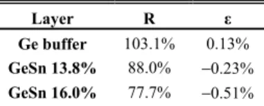
The GeSn heterostructure was grown in a 200 mm Epi Centura 5200 Reduced Pressure – Chemical Vapor Deposition cluster tool from Applied Materials, using Ge2H6, SnCl4 and Si2H6 as precursor gases. GeSn layers were grown on top of a 2.5 µm thick Ge strain relaxed buffer (SRB), which was itself deposited on top of a Si (001) substrate. Ge2H6 and SnCl4 fluxes were fixed and the temperature gradually lowered – from 349°C down to 313°C - during the growth at 100 Torr to create discrete Sn concentration steps, known as “GeSn step-graded epitaxy” in [16,19,20]. Such a strategy limits the number of threading dislocations propagating towards the optically active GeSn 16.0% layer and relaxes it partially. The temperature was slightly increased after the deposition of the GeSn 16.0% layer to grow the GeSn 13.8% top barrier. A temperature of 349°C was used, together with Si2H6, to grow thin SiGeSn electronic barriers which encapsulated the whole GeSn heterostructure. Our aim was to limit electronic recombination on the top surface (top barrier) and potential scattering of carriers in the Ge buffer underneath (bottom barrier). ω-2ϴ scans around the (004) X-ray diffraction (XRD) order, along with Reciprocal Space Mapping (RSM) around the asymmetrical (224) XRD order [Figs. 1(a) and 1(b)] were used to calculate the Sn content, the macroscopic degree of strain relaxation R (%) and the strain value ε (%) in the Ge buffer, GeSn 13.8% and GeSn 16.0% layers, where the diffraction peaks are clearly resolved. Values are given in Table 1, showing a slightly tensile-strained Ge SRB and still compressively-strained GeSn 13.8% and 16.0% layers. The formula used in these calculations were taken from [19,21]. The macroscopic degree of strain relaxation and the Sn concentration for the GeSn 13.8% layers should be interpreted here as a mean value for the bottom and the top GeSn 13.8% layers, as we cannot distinguish in XRD one from the other. ω-2ϴ scan shows four GeSn peaks - corresponding to the four different concentrations present in the active layer/step-graded buffer - with two clearly resolved GeSn 13.8% and GeSn 16.0% layer peaks. Those layers are indeed thicker and of better crystalline quality than the GeSn 8% and 10% layers underneath (lower intensity, broader peaks in XRD). This interpretation was supported with Transmission Electron Microscopy (TEM) images, shown in Fig. 1(c), showing a dense array of misfit dislocations in the GeSn 8% and 10% layers - contrasting with the crystalline quality of the optically active GeSn 16.0% layer and of the GeSn 13.8% layers below and above, confirming the efficiency of the step-graded epitaxy technique. We extracted the thicknesses of GeSn/SiGeSn layers from the TEM image in Fig. 1(d): The optically active GeSn 16.0% layer was 418 nm thick. Based on a recent study on the growth kinetics of SiGeSn thin layers at 349°C [22], we would expect the Si and Sn contents in the bottom SiGeSn layer to be close to 9% and 8%, respectively. Strain relaxation that occurred during the growth of the step-graded structure might have had an impact on the composition of the top SiGeSn layer (which was deposited with exactly the same parameters of the bottom one). In other words, the Si and Sn contents of the top SiGeSn layer might be different from the 9% and 8% nominal values, but precise values are hard to determine experimentally (we would for instance expect the Sn content to be a few percent higher, based on what we know on Sn enrichment in plastically relaxed layers).
Fig. 1. (a) ω-2ϴ scan around the (004) XRD order of the GeSn/SiGeSn heterostructure, grown on a Ge SRB. (b) RSM around the asymmetrical (224) XRD order. (c),(d) Cross-sectional TEM images of the stack, showing in (c) the array of misfit dislocations in the lower part of the GeSn step-graded buffer. Red markers are provided for a better visualization of the interfaces. The thickness of each layer is provided in (d).
Table 1. Macroscopic degree of strain relaxation and strain level in the heterostructure. The Ge buffer is slightly tensile strained while GeSn 13.8% and 16.0% layers are still
compressively strained Layer R ε Ge buffer 103.1% 0.13% GeSn 13.8% 88.0% −0.23% GeSn 16.0% 77.7% −0.51%
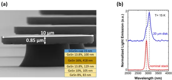
The micro-disk cavity pattern was then transferred to the GeSn heterostructure material stack using e-beam lithography, followed by an anisotropic etching in a Cl2 plasma. The Ge buffer and the bottom SiGeSn layer were then fully etched, while the GeSn layer with the lowest Sn concentration (8%) was partially etched using an isotropic CF4 – dry etch recipe [23,24]. The final thickness of the micro-disk is equal to 850 nm, as shown in Fig. 2(a). Based on layer thicknesses measured from the TEM image, the micro-disk cavity is made of (from
top to bottom) 15 nm of SiGeSn, 100 nm of GeSn 13.8%, 418 nm of GeSn 16.0% (the optically active layer), 129 nm of GeSn 13.8%, 105 nm of GeSn 10% and finally 83 nm of GeSn 8%. We compared the PL signal under continuous excitation of a 20 µm diameter micro-disk (not shown here) - using the fabrication process described above - with the PL signal of the nominal stack. Since the laser spot diameter was 20 µm, we slightly shifted the alignment between the spot and the micro-disk to make sure the perimeter area was well covered. Results are shown in Fig. 2(b), with a shift towards higher wavelength for the micro-disk – which is due to strain relaxation because of the under-etch of the Ge buffer. A shoulder peak at the same wavelength than that of the spectrum of the nominal stack can also be spotted, which likely comes from the center area of the micro-disk, where the Ge pillar is present. All the lasing characterizations that follow were performed on a 10 µm diameter micro-disk.
Fig. 2. (a) Tilted view (SEM) image of GeSn heterostructure micro-disk cavities with the measured diameter and thickness. The calculated concentration and thickness of each layer after the under-etching step are provided in the inset. (b) PL signal under continuous excitation of a 20 µm micro-disk (blue) and the nominal stack (red), with a shift toward higher wavelength due to strain relaxation in the perimeter area.
3. Optical characterization results and discussion
3.1 Optical characterization results
The GeSn heterostructure micro-disk cavity was optically pumped with a pulsed 1064 nm Nd:YAG laser, with a repetition rate of 51 kHz and 0.6 ns pulse width. The laser beam was focused on the sample with a Cassegrain reflective objective, and the same objective was used to collect the PL signal. Absorptive optical density filters were used to modify the pumping power. The signal was analyzed by a Fourier transform infrared (FTIR) spectrometer, equipped with an InSb photodetector to record the PL signal. The PL setup provided an excitation spot of 20 µm diameter, large enough to cover the entire micro-disk cavity surface.
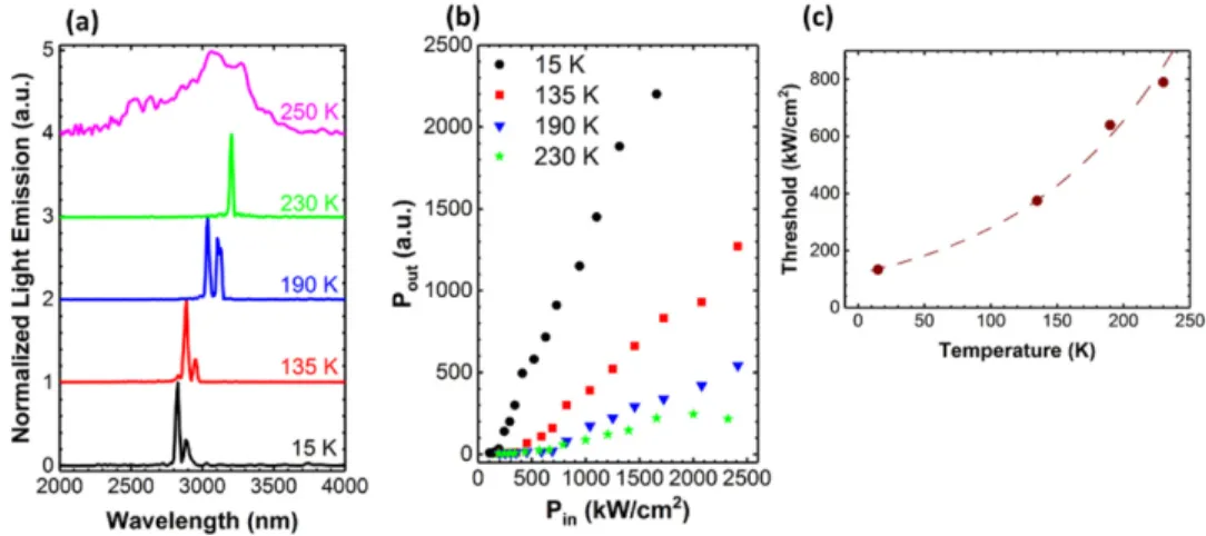
Figure 3(a) shows the evolution of lasing spectra at different temperatures. As temperature increased, a clear red-shift was observed, due to the reduction of the GeSn band gap. Only the spontaneous PL background was observed once the temperature reached 250 K, where the modal gain was not high enough for lasing. Figure 3(b) shows the Pin-Pout characteristics of the GeSn micro-disk cavity at temperatures from 15 K to 230 K. The spontaneous and the lasing regime, with a linear increase of Pout versus Pin, are clearly distinguished. At 15 K, 135 K and 190 K, the lasing thresholds - calculated from an extrapolation of the lasing regime to Pout = 0 – are 134 kW/cm2, 375 kW/cm2 and 640 kW/cm2, respectively. Figure 3(c) shows the
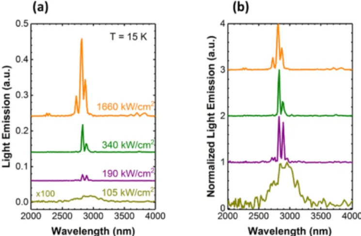
exponential fit for the variation of threshold as function of temperature. We extracted from that fit a 117 K nominal characteristic temperature for our GeSn micro-disk laser. Figures 4(a) and 4(b) show the evolution of the lasing spectra at 15 K with the pumping powers: Below the threshold (105 kW/cm2), only a broad spontaneous PL background is observed. Spectra above threshold show multimode lasing, with two lasing peaks (2825, 2890 nm) at medium pumping powers (190 - 340 kW/cm2). At high pumping power (1660 kW/cm2), an additional lasing mode appears at 2720 nm. Compared to lower temperatures, the onset of lasing is more gradual at 230 K. Here, the extrapolation method can somewhat underestimate the lasing threshold of the micro-disk cavity. Figure 5(a) and 5(b) show the spectrum at 660 kW/cm2. Although the pumping power is well above the threshold value given by the extrapolation (503 kW/cm2), only a broad spontaneous PL spectrum was observed instead of a narrow lasing peak. In this case, the transformation of the spectrum shape should be used to estimate the lasing threshold. Starting from 790 kW/cm2, a narrow lasing peak appears at 3200 nm. 790 kW/cm2 is therefore the upper limit of the lasing threshold at 230 K for our GeSn 16.0% heterostructure micro-disk cavity.
Fig. 3. (a) Lasing spectra at 15 K, 135 K, 190 K and 230 K. Only a PL background was observed at 250 K. The lasing spectra shown here were obtained at different pumping powers, highlighting the clearly resolved lasing peaks and the wavelengths shift. (b) Pin – Pout curves at
15 K, 135 K, 190 K and 230 K. c) The exponential fit curve to the variation of threshold as a function of temperature yielded a nominal characteristic temperature T0 = 117 K
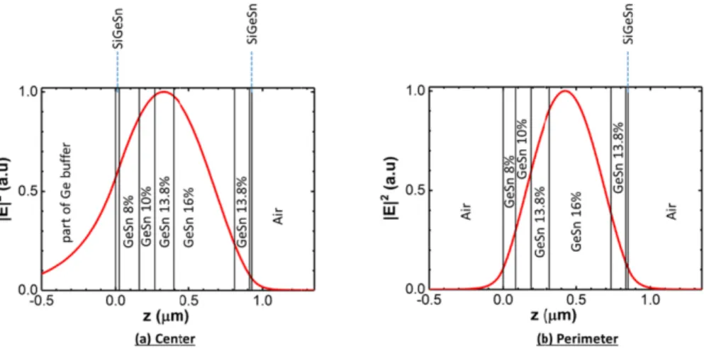
Fig. 4 kW/cm Norm Fig. 5 kW/cm sponta power 3.2 Discussi The maximum - 17.5% opti temperature i 16.0% layer ( 260 nm of Ge in the under-e modes in a s perimeter of t in our previou GeSn 16.0% the optical fie 6(b)]. We to ellipsometry m
4. (a) Lasing spectr m2 is magnified 10
malized spectra at s
5. (a) Lasing spectr m2 and 790 kW/c aneous emission rs ion m lasing tempe cal cavities (2 mprovement b (418 nm) used eSn 17.5% in [ etched micro-d lab waveguide the micro-disk usly reported G layer is higher eld decays into ook as refract measurement [
ra of the GeSn het 00-folds to show t ame pumping pow
ra of the GeSn he cm2 are magnified
and the lasing re
erature is here 5 230 K compar by differences here was thick [17]. The optic disk cavity hig e gives a conf k, which is sign GeSn 16.0% m r in the perime o the thick Ge tive index, nG [25]. We other terostructure micro the broad PL back wers terostructure micr d 10-folds, showin egime (b) Normal 50 K higher tha red to 180 K) in material sta ker than the 18 cal confinemen gher. Simulatio finement factor nificantly highe micro-disk [16].
eter than in the buffer undern Ge = 4 and n rwise, assumed o-disk at 15 K. Th kground, where no ro-disk at 230 K. T ng a switch betwe lized spectra at th an in previous ) [16,17]. We acks. First, the 81 nm of GeSn nt is thus stron on using a 1D r of 63% for t er than the 38. . The confinem e center area o neath in the lat
nGeSn = 4.2 b d that the refr
he spectrum at 105 o lasing occurs. (b)
The spectra at 660 een the regime of he same pumping
reports on GeS explain such e optically acti n 16.0% in [16 nger and the m D model for TE
the electric fie .2% confineme ment factor in t
of the micro-di tter case [Figs. based on spec ractive index d 5 ) 0 f g Sn 16.0% a lasing ive GeSn 6] and the modal gain E0 guided eld in the ent factor the active isk, since 6(a) and ctroscopic difference
between GeSn layers of different Sn contents and SiGeSn layers was very small. In addition, there is a GeSn 13.8% / SiGeSn stack on top of the active layer, which was not present in [16] and [17] stacks. Such layers likely act as additional electronic potential barriers, confining the carriers in the optically active GeSn 16.0% layer. The bottom low concentration GeSn buffer did not contribute to that improvement; indeed, the very same GeSn buffer structure was used in [16]. The bottom SiGeSn layer is still present in the center of the micro-disk. Meanwhile, it was fully etched in the outer parts of the suspended micro-disks. The bottom SiGeSn layer therefore acts, in the center of the disk, as an electronic barrier between the Ge buffer and the optically active GeSn layers. However, since the favorable modes for lasing in such cavities are whispering gallery modes (WGM) – which are located mostly in the perimeter of such micro-disks, the efficiency of the bottom SiGeSn layer in the current configuration is questionable. Improving in the future the etching selectivity between Ge and GeSn/SiGeSn and thereby keeping the bottom SiGeSn layer intact during the fabrication process should help in answering that question. In addition, with the current material structure, we are still unable to decouple contributions from optical confinement and electronic confinement. A micro-disk cavity fabricated with a similar stack, this time without the top GeSn 13.8% / SiGeSn bi-layer, should be investigated to answer this question.
We can compare the low temperature threshold of this GeSn 16.0% micro-disk to literature values for the same kind of cavities. The current threshold, 134 kW/cm2 at 15 K, is nearly three times lower than the one we recently published on GeSn 16.0% graded-buffer micro-disks [16] without any GeSn 13.8% / SiGeSn barriers (377 kW/cm2 at 25 K) [16]. A 10K difference cannot explain such drastic threshold changes. We indeed obtained at 135K a threshold value of 375 kW/cm2, i.e. almost the 25 K value in [16]. An optical confinement improvement because of the use of a thicker GeSn 16.0% active layer and a carrier confinement stemming from the presence of the GeSn 13.8% / SiGeSn bi layer on top of our micro-disk most likely explains, besides the 50K increase in the maximum lasing temperature, why we had this nearly three times reduction of the low temperature threshold.
Our 15K threshold is otherwise very close to that reported for lower Sn concentration GeSn micro-disks in [15] (130 kW/cm2 at 20 K for 12.5% of Sn). One would expect a lower lasing threshold in higher GeSn micro-disk cavities, given the higher gap between Γ and L valleys. Higher Sn concentration GeSn layers might however be of lesser quality as they are more metastable (higher risks of having Sn nano-precipitates and other defects in the optically active layers). This would have a harmful impact on laser performances. Significantly lower thresholds (45 kW/cm2 at 20 K) were recently obtained in micro-disks with GeSn 13.0% multi quantum wells (MQW) [18]. This might be a path forward for a future optimization of GeSn 16.0% micro-disk performances.
Being able to grow SiGeSn barrier layers beneath and just above GeSn 16.0% optically active layers would then be mandatory. This would be difficult because of thermal budget and Sn segregation issues. Indeed, the SiGeSn barrier layers were grown here at 349°C, while the optically active GeSn 16.0% layer was grown at 313°C only. A 37°C temperature difference would have a huge impact on Sn segregation (Sn droplet formation on the surface). We indeed noticed that the surface of thick GeSn 16.0% layers was very unstable. Such layers had to be capped with lower tin content layers without any growth interruption, which would have been mandatory during the temperature ramping-up prior to SiGeSn encapsulation. We have however progressed concerning the growth of SiGeSn layers at various temperatures and should be able, in the near future, to grow SiGeSn barriers beneath and just above such GeSn 16.0% layers [26].
Fig. 6 the ce interfa the re nGeSn = 4. Conclusio In summary, optically activ readily acces threading dis discrete conc wavelengths performances elevated maxi better carrier find a strategy References 1. A. Georgakil “Generation J. Mater. Res 2. K. Morizane Growth 38(2 3. Y. Bogumilo X. Bao, Z. Y silicon subst 4. D. Zubia and the heteroepi 5. J. Z. Li, J. Ba by aspect rat 6. H. Schmid, M assisted selec Phys. Lett. 1 7. M. Knoedler “Observation Res. 17(12), 8. J. Liu, X. Su gain medium 9. M. de Kersau Sagnes, and 19(19), 1792 6. Optical confinem enter of the micro
ace between the Si emaining GeSn 8% = 4.2 and nSi = 3.4
on
we demonstra ve GeSn 16.0% sible with two slocations in t
centration step ranging from , with a low la imal lasing tem confinement. F y to further imp las, J. Stoemenos, and annihilation o s. 8(08), 1908–192 e, “Antiphase doma 2), 249–254 (1977) owicz, J. M. Hartm Ye, and E. Sanchez rates,” Appl. Phys d S. D. Hersee, “N itaxy of mismatch ai, C. Major, M. C tio trapping,” J. Ap M. Borg, K. Mosel ctive epitaxy of III 06(23), 233101 (2 r, N. Bologna, H. S n of Twin-free GaA
6297–6302 (2017 un, D. Pan, X. Wan m for monolithic la uson, M. El Kurdi P. Boucaud, “Opti 25–17934 (2011).
ment in the z-direc o-disk and (b) the iGeSn layer and th % layer in case (b) . ated that a Ge % layer can la o-stage thermo the optically a ps. Spectrally m 2720 nm asing threshold mperature (230 Future work w prove GeSn las
K. Tsagaraki, P. K of antiphase domai 21 (1993). ain structures in G ). mann, R. Cipro, R. z, “Anti-phase bou s. Lett. 107(21), 21 Nanoheteroepitaxy: ed semiconductor Carroll, A. Lochtef ppl. Phys. 103(10) lund, L. Gignac, C I–V nanoscale dev 2015). Schmid, M. Borg, As Nanowire Grow 7). ng, L. C. Kimerlin aser integration on , S. David, X. Che ical gain in single
ction (perpendicula perimeter of the he Ge buffer under ). We used as refr eSn heterostru ase up to 230 o-electric Pelti active layer, w multimode l to 3200 nm d at low temp K), came from will aim to dec sing performan
Komninou, N. Flev in boundaries in G GaP and GaAs epita
Alcotte, M. Marti undaries–Free GaA
12105 (2015). The Application materials,” J. App feld, and Z. Shellen ), 106102 (2008). C. M. Breslin, J. Br vices for co-planar
K. Moselund, S. W wth Using Templa g, T. L. Koch, and Si,” Opt. Express ecoury, G. Fishman
tensile-strained ge
ar to the surface of micro-disk. The z rneath in case (a), ractive indexes nai ucture micro-di K. Such oper ier coolers. T we used a ste lasing was ob m. The state-erature (134 k m a stronger op ouple the cont nces.
varis, P. Panayotat GaAs on Si grown b
taxial layers grown in, F. Bassani, J. M As epilayers on “qu of nanostructuring pl. Phys. 85(9), 64 nbarger, “Defect r ruley, D. Cutaia, a r heterogeneous in Wirths, M. D. Ros ate-Assisted Select d J. Michel, “Tensi 15(18), 11272–11 an, S. Sauvage, R. ermanium photoni
f each layer) at (a) z = 0 point is the and the bottom of
ir = 1.0, nGe = 4.0
isk cavity with rating tempera To limit the nu ep-graded epit bserved, with of-the-art Ge kW/cm2 at 15K ptical confinem tribution from
tos, and A. Christo by molecular beam n on Si and Ge,” J. Moeyaert, T. Baron uasi-nominal” Ge-g and substrate com 492–6496 (1999).
reduction of GaAs and H. Riel, “Temp ntegration with Si,” sell, and H. Riel, tive Epitaxy,” Cry ile-strained, n-type 1277 (2007).
Jakomin, G. Beau ic wire,” Opt. Expr
) e f , h a thick atures are umber of taxy with h emitted eSn laser K) and an ment and a each and ou, m epitaxy,” . Cryst. n, J. B. Pin, -buffered mpliance to /Si epitaxy plate-” Appl. yst. Growth. e Ge as a udoin, I. ress
10. D. Nam, D. S. Sukhdeo, J. H. Kang, J. Petykiewicz, J. H. Lee, W. S. Jung, J. Vučković, M. L. Brongersma, and K. C. Saraswat, “Strain-Induced Pseudoheterostructure Nanowires Confining Carriers At Room Temperature with Nanoscale-Tunable Band Profiles,” Nano Lett. 13(7), 3118–3123 (2013).
11. M. J. Suess, R. Geiger, A. R. Minamisawa, G. Schiefler, J. Frigerio, D. Chrastina, G. Isella, R. Spolenak, J. Faist, and H. Sigg, “Analysis of enhanced light emission from highly strained germanium microbridges,” Nat. Photonics 7(6), 466–472 (2013).
12. A. Gassenq, K. Guilloy, G. Osvaldo-Dias, N. Pauc, D. Rouchon, J. M. Hartmann, J. Widiez, S. Tardif, F. Rieutord, J. Escalante, I. Duchemin, Y.-M. Niquet, R. Geiger, T. Zabel, H. Sigg, J. Faist, A. Chelnokov, V. Reboud, and V. Calvo, “1.9% bi-axial tensile strain in thick germanium suspended membranes fabricated in optical germanium-on-insulator substrates for laser applications,” Appl. Phys. Lett. 107(19), 191904 (2015). 13. S. Wirths, R. Geiger, N. von den Driesch, G. Mussler, T. Stoica, S. Mantl, Z. Ikonic, M. Luysberg, S. Chiussi, J.
M. Hartmann, H. Sigg, J. Faist, D. Buca, and D. Grutzmacher, “Lasing in direct-bandgap GeSn alloy grown on Si,” Nat. Photonics 9(2), 88–92 (2015).
14. S. Al-Kabi, S. A. Ghetmiri, J. Margetis, T. Pham, Y. Zhou, W. Dou, B. Collier, R. Quinde, W. Du, A. Mosleh, J. Liu, G. Sun, R. A. Soref, J. Tolle, B. Li, M. Mortazavi, H. A. Naseem, and S.-Q. Yu, “An optically pumped 2.5 μm GeSn laser on Si operating at 110 K,” Appl. Phys. Lett. 109(17), 171105 (2016).
15. D. Stange, S. Wirths, R. Geiger, C. Schulte-Braucks, B. Marzban, N. von den Driesch, G. Mussler, T. Zabel, T. Stoica, J. M. Hartmann, S. Mantl, Z. Ikonic, D. Grutzmacher, H. Sigg, J. Witzens, and D. Buca, “Optically Pumped GeSn Microdisk Lasers on Si,” ACS Photonics 3(7), 1279–1285 (2016).
16. V. Reboud, A. Gassenq, N. Pauc, J. Aubin, L. Milord, Q. M. Thai, M. Bertrand, K. Guilloy, D. Rouchon, J. Rothman, T. Zabel, F. Armand Pilon, H. Sigg, A. Chelnokov, J. M. Hartmann, and V. Calvo, “Optically pumped GeSn micro-disks with 16% Sn lasing at 3.1 μm up to 180 K,” Appl. Phys. Lett. 111(9), 092101 (2017). 17. J. Margetis, S. Al-Kabi, W. Du, W. Dou, Z. Yiyin, T. Pham, P. Grant, S. A. Ghetmiri, M. Aboozar, B. Li, J. Liu,
G. Sun, R. A. Soref, J. Tolle, M. Mortazavi, and S.-Q. Yu, “Si-Based GeSn Lasers with Wavelength Coverage of 2–3 μm and Operating Temperatures up to 180 K,” ACS Photonics 5(3), 827–833 (2018).
18. D. Stange, N. von den Driesch, D. Rainko, T. Zabel, and B. Marzban, Z. ikonic, P. Zaumseil, G. Capellini, S. Mantl, J. Witzens, H. Sigg, D. Grutzmacher, and D. Buca “Quantum Confinement Effects in GeSn/SiGeSn Heterostructure Lasers,” in 2017 IEEE International Electron Devices Meeting (2017), paper 24.2.1.
19. J. Aubin, J. M. Hartmann, A. Gassenq, J. L. Rouvière, E. Robin, V. Delaye, D. Cooper, N. Mollard, V. Reboud, and V. Calvo, “Growth and structural properties of step-graded, high Sn content GeSn layers on Ge,” Semicond. Sci. Technol. 32(9), 094006 (2017).
20. S. Takeuchi, Y. Shimura, O. Nakatsuka, S. Zaima, M. Ogawa, and A. Sakai, “Growth of highly strain-relaxed Ge1-x Snx/virtual Ge by a Sn precipitation controlled compositionally step-graded method,” Appl. Phys. Lett. 92(23), 231916 (2008).
21. F. Gencarelli, B. Vincent, J. Demeulemeester, A. Vantomme, A. Moussa, A. Franquet, A. Kumar, H. Bender, J. Meersschaut, W. Vandervorst, R. Loo, M. Caymax, K. Temst, and M. Heyns, “Crystalline Properties and Strain Relaxation Mechanism of CVD Grown GeSn,” ECS J. Solid State Sci. Technol. 2(4), 134–137 (2013). 22. R. Khazaka, J. Aubin, E. Nolot, and J. M. Hartmann, “Investigation of the Growth of Si-Ge-Sn Pseudomorphic
Layers on 200 mm Ge Virtual Substrates: Impact of Growth Pressure, HCl and Si2H6 Flows”, accepted for
publication in ECS Transactions - G03 Symposium, AIMES 2018 Meeting of the Electro-Chemical Society (30 September – 4 October 2018).
23. S. Gupta, R. Chen, Y. C. Huang, Y. Kim, E. Sanchez, J. S. Harris, and K. C. Saraswat, “Highly Selective Dry Etching of Germanium Over Germanium-Tin (Ge1-xSnx): A Novel Route for Ge1-xSnx Nanostructure
Fabrication,” Nano Lett. 13(8), 3783–3790 (2013).
24. L. Milord, J. Aubin, A. Gassenq, S. Tardif, K. Guilloy, N. Pauc, J. Rothman, A. Chelnokov, J. M. Hartmann, V. Calvo, and V. Reboud, “GeSn lasers for mid-infrared silicon photonics,” Proc. SPIE 10108, 105370S (2018). 25. CEA, unpublished.
26. R. Khazaka, E. Nolot, J. Aubin, and J.M. Hartmann, “Growth and characterization of SiGeSn pseudomorphic layers on 200 mm Ge virtual substrates,” submitted for publication in Semicond. Sci. Technol. (June 2018).