A cuttable multi-touch sensor
The MIT Faculty has made this article openly available. Please share
how this access benefits you. Your story matters.
Citation
Olberding, Simon, Nan-Wei Gong, John Tiab, Joseph A. Paradiso,
and Jürgen Steimle. “A Cuttable Multi-Touch Sensor.” Proceedings
of the 26th Annual ACM Symposium on User Interface Software
and Technology - UIST ’13 (2013), October 8–11, 2013, St. Andrews,
United Kingdom, ACM.
As Published
http://dx.doi.org/10.1145/2501988.2502048
Publisher
Association for Computing Machinery
Version
Author's final manuscript
Citable link
http://hdl.handle.net/1721.1/92396
Terms of Use
Creative Commons Attribution-Noncommercial-Share Alike
A Cuttable Multi-touch Sensor
Simon Olberding
1, Nan-Wei Gong
2, John Tiab
1, Joseph A. Paradiso
2, Jürgen Steimle
11
Max Planck Institute for Informatics
Campus E1 7, 66123 Saarbrücken, Germany
{solberdi, jtiab, jsteimle}@mpi-inf.mpg.de
2
MIT Media Lab
75 Amherst Street, Cambridge MA 02142, USA
{nanwei, joep}@media.mit.edu
ABSTRACT
We propose cutting as a novel paradigm for ad-hoc custom-ization of printed electronic components. As a first instanti-ation, we contribute a printed capacitive multi-touch sensor, which can be cut by the end-user to modify its size and shape. This very direct manipulation allows the end-user to easily make real-world objects and surfaces touch-interactive, to augment physical prototypes and to enhance paper craft. We contribute a set of technical principles for the design of printable circuitry that makes the sensor more robust against cuts, damages and removed areas. This in-cludes novel physical topologies and printed forward error correction. A technical evaluation compares different to-pologies and shows that the sensor remains functional when cut to a different shape.
Author Keywords
Cuttable Electronics, Printed Electronics, Multi-touch Sen-sor, Capacitive Sensing, Ubiquitous Computing.
ACM Classification Keywords
H.5.2. Information interfaces and presentation (e.g., HCI): General Terms
Human Factors; Design; Measurement. INTRODUCTION
Conventional electronic components and devices cannot be cut to customize their size and shape in an ad-hoc manner. Their rigid substrate is hard to cut, components are too ex-pensive to be discarded and cutting irreversibly damages the electronic circuit. In contrast, people have always cut traditional materials for tailoring them to their specific needs. At home, people wrap packages with material, which is cut to shape; they cut protective films to cover books and devices of various sizes; and they create artistic shapes in paper craft. At the workplace, tailors cut textiles to fit the
size of the customer, carpenters cut wood to build furniture, and designers or engineers cut cardboard and plywood to create physical prototypes.
This form of very direct manipulation enables people to quickly and easily create custom shapes and objects; in ad-dition the direct manual interaction with the material en-courages thinking by doing [7].
Printed electronics now enables for a novel paradigm, in-troduced in this paper: printed electronic components and devices can easily be tailored to a custom shape and size by ad-hoc cutting. This is possible because substrates are very thin and flexible, and printouts are cheap. However, current printed solutions take over the circuitry schemes from con-ventional electronics. Due to its internal layout, cutting parts off to adapt the shape will very likely break the elec-tronics. Therefore we advocate that printed electronics re-quires novel electronic designs that can cope with its new material properties: designs that are robust against cuts and removed areas of the substrate.
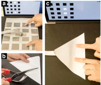
Figure 1: We contribute technical principles and an imple-mentation of cut-robust printed multi-touch sensor sheets. a) The multi-touch sensor features a novel wiring scheme. b) This allows to sensor to be cut very much like a
conven-tional material while (c) remaining touch-sensitive.
Permission to make digital or hard copies of all or part of this work for personal or classroom use is granted without fee provided that copies are not made or distributed for profit or commercial advantage and that copies bear this notice and the full citation on the first page. Copyrights for components of this work owned by others than ACM must be honored. Abstracting with credit is permitted. To copy otherwise, or repub-lish, to post on servers or to redistribute to lists, requires prior specific permission and/or a fee. Request permissions from [email protected].
UIST’13, October 8–11, 2013, St. Andrews, United Kingdom.
Copyright © 2013 ACM 978-1-4503-2268-3/13/10…$15.00.
As a first instantiation of this paradigm, we contribute a printed capacitive multi-touch sensor, which the user can tailor by cutting it to the desired size and shape (see Fig. 1). We present technical principles that make the circuit layout more robust against physical cuts and removed areas, taking inspiration from topology in biological systems and com-puter networks, as well as from coding theory. First, we contribute novel topologies for the circuit layout that are more robust against cuts. Second, we show how by
combin-ing several topologies in the same sensor sheet, a wider
variety of cut-out shapes can be supported. Third, we con-tribute a principle for adding various levels of redundancy within each topology, proposing printed forward error
cor-rection.
We validate our technical contributions by a detailed
simu-lation, an evaluation of the electronic sensing properties,
and a proof-of-concept implementation of several letter-sized cuttable sensor sheets.
TOWARDS CUTTABLE MATERIALS WITH EMBEDDED MULTI-TOUCH SENSING
Our vision is that printed sensors will be so inexpensive that multi-touch sensing capability will become an inherent part of the material. For instance, manufacturers of protective foils will offer a product line that features multi-touch sens-ing. Paper manufacturers will offer paper, cardboard or adhesive labels, which have the printed multi-touch sensor embedded. Manufacturers of wooden boards will offer boards that feature the sensor. The user buys the material in one of several standard sizes and then cuts it to the desired size and shape, using tools such as scissors, razors, saws, or laser cutters. This very direct physical manipulation seam-lessly integrates with existing practices for customization, prototyping and crafting. It stands in contrast with existing solutions, which either require the additional a step of de-signing the sensor at a computer [21] or by requiring an expert to design a customized sensing solution.
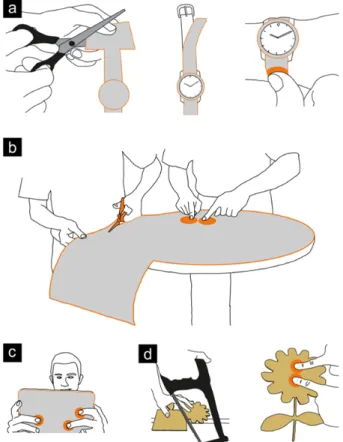
Cuttable multi-touch sensor foils, sheets and boards will be a ubiquitous resource, enabling a wide range of applica-tions. For ubiquitous computing, people can easily add mul-ti-touch input on pretty much any physical object or sur-face, by using an adhesive multi-touch foil that is cut to match the desired size and shape. As illustrated in Fig. 2 a-c, this enables people to easily touch-augment physical ob-jects and devices. In prototyping and crafting,
touch-enabled paper, cardboard or plywood empowers people to
make models, prototypes and artwork interactive (Fig. 2d). RELATED WORK
Shape-adaptable Multi-touch Sensors
The commonly used principle for the construction of a mul-ti-touch sensor [17,22,28,20,11,4,18] is illustrated in Fig. 3. A set of electrodes is arranged on a regular two-dimensional grid. Each electrode senses one touch point. The electrodes are connected to a controller with a set of horizontal and parallel wires; each electrode is situated at the intersection of one horizontal and one parallel wire.
Therefore it can be uniquely addressed by the appropriate combination of two wires. The elegance of this approach is in requiring only a minimum number of wires. However, this grid topology is not designed for shape adaptation. It is not robust to cuts and removed parts. Since each wire ad-dresses many electrodes, damage of a wire results in a burst effect: many electrodes become unusable and possibly large areas of the sensor stop working. Moreover, the controller connects to the sensor from its outer sides; in consequence these sides cannot be removed, preventing round shapes. Some prior work has investigated means to realize shape-adaptable sensors. Additive approaches support shape cus-tomization by combining
multiple interconnected active sensor tiles or nodes [4,12,14,15,19]. Subtractive approaches support customization by cutting. Our work draws inspiration from work by Wimmer et al. [31] and Holman et. al [8], who introduced cutting of a sensor strip for adapting its length. Wimmer et al.’s sensor is adapted in
Figure 3: Concept of a tradi-tional multi-touch pad. Figure 2: a-c) Easily touch-enable objects with a cuttable multi-touch foil. d) Build interactive objects, prototypes or
shape by cutting a sensor wire to the desired length and laying it out using a space-filling curve. Alternatively, sev-eral prefabricated sensor tiles, each containing a wire, can be combined. While this elegant solution supports virtually any sensor shape, it is limited to single-touch input and re-quires a complicated sensing technology, Time Domain Reflectometry. Tekscan[24] developed a pressure sensitive shoe inlet that can be trimmed to fit different sizes. While the size can be varied, the shape itself is predefined due to the internal wiring. We extend upon prior work by contrib-uting the first cuttable multi-touch sensor sheet.
Printed Electronics
Printed electronics is the key enabling technology for the approach presented in this paper, as this technology allows producing sensitive surfaces in large scale at very low cost and on a very thin substrate [25]. While inkjet printing of electronics [25] enables customized electronic circuits in small quantities, roll-to-roll printing [25] supports large sizes and high printing speeds. It is possible to print multi-layered electronic circuits and active electronic compo-nents, such as transistors, by combining conductive, semi-conductive and insulating inks on several layers [25]. While such active electronics are still on the level of basic re-search, printing of passive conductive circuits is already commercially offered [3]. To keep costs low and to enable a deployment in the near future, our solution only requires passive printed electronics.
Rapid Prototyping
Our work is also heavily inspired from prior research on rapid prototyping. A stream of previous work allows the user to make a physical prototype interactive. For instance, this is done by attaching electronic components on the pro-totype and connecting them by drawing conductive traces with a conductive pen [29], or by attaching thin lines of copper [16]. As an alternative to hand-drawn traces, Vo-dooIO [27] introduced a specific foam substrate that wires electronic components that the user attaches on the materi-al. This stream of work emphasizes on the importance of hand-crafting in rapid prototyping.
Another stream of research proposes digital fabrication [30,13] for creating interactive prototypes [9,21]. The Midas toolkit [21] enables the user to digitally design a custom touch sensor on a computer. The sensor then gets produced on a vinyl cutter and can be attached onto the object.
Our approach complements the above work in two ways. Using physical tools (such as scissors, knife or saw), the sensor can be iteratively customized in its shape before, during and after the crafting process. This contrasts with previous work [21] in which the sensor cannot be altered once it is designed and printed. But our approach also ex-tends digital prototyping in the way that the user can plan digitally and then use a machine to cut the sensor sheet or sensor-enabled material into a desired shape.
REQUIREMENTS
Multi-touch sensors must fulfill a set of technical require-ments, such as a specific spatial and temporal resolution, dynamic range and number of touch points. Shape-adaptable multi-touch sensors extend this set with several additional requirements that are specific to cutting. We identify four desirable properties, which a cuttable sensor sheet ideally should fulfill. Taken together, they define what is intuitively understood by “robustness” of the sensor to cutting.
Set of supported shapes: The sensor should support a
large set of cut-out shapes, including convex and non-convex shapes. This means that all electrodes on the cut-out shape remain functioning.
Scale and aspect ratio invariance: The cut-out shape can
be of any size and aspect ratio, as long as it fits on the sheet. Besides these intrinsic properties of the shape, extrinsic characteristics are affected by where and how the shape is placed on the sensor sheet:
Rotation invariance: A specific shape should be supported
no matter in which orientation it is placed on the sensor sheet.
Location invariance of the connector: The sensor sheet
has a connector to tether it with the controller. It should be possible to locate this connector at several locations or even any location on the cut-out shape, to integrate well with the specific requirements of the application.
While a working solution does not have to support all of these requirements, supporting more of them increases its usability, as the user can cut a wider variety of shapes and place them more freely on the sensor sheet.
In the following sections, we contribute three principles to create more robust multi-touch sensors that better fulfill the above requirements.
TOPOLOGIES FOR CUTTABLE MULTI-TOUCH SENSORS Multi-touch sensors are typically based on a matrix topolo-gy. As we have discussed in the related work section, this topology is not robust to cuts and removed areas and does not support a variety of cut-out shapes. In this section, we introduce novel basic wiring topologies for cuttable multi-touch sensors that are inspired by biological systems and computer networks. We show how they improve the ro-bustness of the sensor against cuts and discuss which cut-out shapes they support.
Radial and tree structures are very common organization principles in biological systems, e.g. in blood and nerve systems, in the physical structure of plants and in fungal structures [6]. This ensures not only effective transmission, but also protects vitally important parts in an inner area of the system. Also in computer networks, star and tree struc-tures are amongst the most central topologies [23]. Meshes are a further promising structure, often applied in computer
networks, which however require active routing compo-nents.
In the following, we present star-based and tree-based to-pologies. Similarly to the conventional matrix topology, they lay out the electrodes on a regular grid. This ensures a consistent spatial resolution across all areas of the sensor. In contrast to the standard matrix topology, they use point-to-point connections between connector and electrodes to avoid burst effects, in which loss of a single wire would result in irreversibly damaging multiple electrodes.
Star Topology
The first layout follows the geometry of a star (Figure 4a). The connector, which is used to tether the sensor sheet with a controller, is placed in the center. Wires extend radially to the electrodes. This topology can be realized with two lay-ers (wires are routed underneath the electrodes with proper shielding) or as a single layer (wires are routed around the electrodes).
The star topology has a number of desirable properties. Due to the circular scheme, all wires run towards the center of the sheet on the shortest path between the electrode and the
connector. This reduces the likelihood of a wire getting cut while the corresponding electrode remains on the sensor. As outlined above, this is a problem of the classical matrix topology, in which an electrode can be affected by a cut at the very other end of the sensor. In the star topology, the electrode and its corresponding wire are always located within the same pie slice. Cuts in the remaining pie slices will never affect the electrode. Another benefit is that the topology is point symmetric. A shape is supported no mat-ter how it is rotated around the controller.
The full set of supported shapes can be mathematically modeled. The outline of the shape is defined by any polar
function defining an
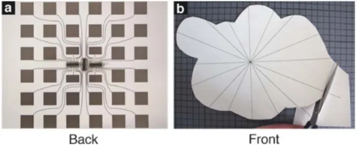
outline that does not extend beyond the sheet (see Fig. 4b). This topology supports a large variety of shapes, including triangles, convex rectangles and ellipses (see Fig. 5a). These shapes can be located anywhere on the sheet as long as the connector is inside the shape (realizing location in-variance). Moreover, the shapes can have arbitrary scale and aspect ratio. The star topology also supports some non-convex shapes, such as “heart-like”, “cloud-like” or “star-like” shapes, provided they are properly placed on the sheet (see Fig. 5b). However, it only partially supports more complex shapes, such as the ones depicted in Fig. 8. We implemented a prototype sensor sheet in letter size, which is based on the star topology and has 36 electrodes (Fig. 6). We printed fine radial lines on the front side to communicate the wiring layout to the user. As a rule of thumb, the shape will be supported if each line is cut not more than once.
Tree topology
In the tree topology, all electrodes are orthogonally con-nected to one stream of wires, which is then concon-nected to the controller (Fig. 6a). Through the indirection in how electrodes are wired with the connector, the tree topology supports shapes that are not supported by the star (and vice versa). This specifically includes shapes that introduce con-cavity, as depicted in Fig. 8a and b. Carve-outs are only partially supported (see Fig. 8c,d).
Figure 6: a) Backside of the fabricated multi-touch sensor featuring a grid of 6x6 electrodes. b) To guide the user, the
front side features fine printed lines.
Figure 4: a) The star topology wires the connector radially with each electrode. b) The star supports shapes with
out-lines that can be defined by any positive polar function (green line). The blue filling indicates functional electrodes.
Figure 5: a) The star topology supports a large variety of convex shapes including triangles, rectangles and ellipses. b)
It also supports shapes that introduce concavity, provided they are properly placed.
The tree is not rotation invariant but supports different sizes and aspect ratios of the cut-out shape. The outline is defined by two continuous functions, whereby the stem of the tree is the x axis (see Fig. 7b).
We implemented a first instantiation of a letter-sized sensor sheet, depicted in Fig. 9. We printed fine lines on the paper to provide guidance about which cuts are supported. ADDING REDUNDANCY BY COMBINING TOPOLOGIES In this section we show how to further increase the robust-ness of the sensor and to support more shapes by combining two or more topologies in one sensor sheet. Since different topologies each have their unique strengths and drawbacks, combining them adds valuable redundancy and geometric robustness. Each electrode is connected to the connector via two or more potentially very different paths. Note that this does not increase the number of pins required at the hard-ware controller, since all wires from all layers that are con-nected to the same electrode are combined at the connector.
Conceptually, we distinguish between two cases: Overlay-ing (1) distinct topologies and/or (2) the same topology: (1) combines the advantages of two distinct topologies. For instance, consider overlaying the star topology with a tree topology. This would support all shapes of Fig. 5 and Fig. 8a,b.
(2) can overcome some limitations, which are inherent to the specific topology, by repeating this topology in a rotated or displaced manner. For instance, consider overlaying two tree layouts rotated by 90 degrees around the center point (see Fig. 10a). This makes the layout invariant to 90 degree Figure 10: a) Overlaying two tree topologies improves rota-tion invariance. b) Overlaying two star topologies allows
for wider range of supported shapes.
Figure 11: Prototype of a dual-layer sensor with overlaid tree and star topologies for a 4x4 sensor sheet. The tree topology is printed on a transparent PET film. Both layers are connected
using 3M conductive z-Tape. Figure 7: a) In the tree topology, all wires are routed to a
central stem. b) The outline of the shape can be defined by two continuous functions. Functional electrodes are blue.
Figure 8: The tree supports carve-outs at the border of a shape (a,b). Puzzle-shaped connection pieces
are partially supported (c,d).
Figure 9: a) Prototype of a multi-touch sensor that imple-ments the tree topology. b) As long as the user does not cut
rotations. Overlaying two star layouts in a displaced man-ner (see Fig. 11b) allows for supporting shapes with certain concave elements, which otherwise would be supported only by the tree (see Fig. 8a, b).
Mathematically, the outline of the shape can be divided in segments. As long as each segment can be represented by a valid function in at least one of the overlaid topologies, the shape is supported.
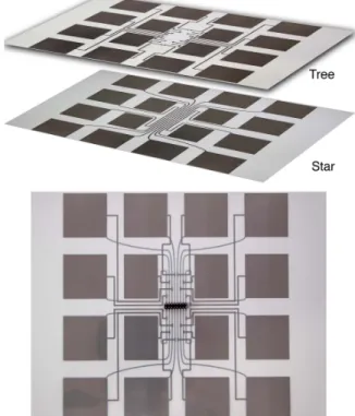
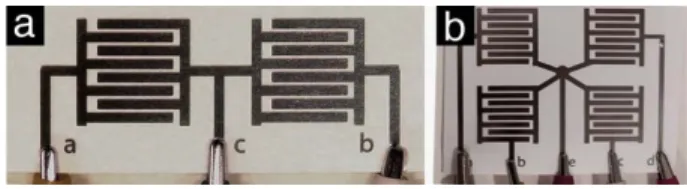
We implemented a first prototype of a sensor with two overlaid topologies, an overlay of a star and a tree. Figure 11a shows how tree and star are overlaid; Figure 11c shows the compound sensor.
INCREASING ROBUSTNESS WITHIN A TOPOLOGY In this section, we contribute methods for encoding redun-dancy within a topology.
Basic Redundant Wiring
Figure 12 (a1) shows an example of an electrode that is cut in two pieces. While a considerable part of the electrode remains on the sensor sheet, it cannot be read, since the wire is cut off. Connecting each electrode with two redun-dant wires from its opposite sides makes the sensor robust to such situations (see Fig. 12 a2)). Moreover, this adds robustness to cases where one of the wires is damaged (see Fig. 12b). This rather simplistic form of redundancy re-quires the double amount of wires.
Printed Forward Error Correction
A more advanced solution adds redundancy with fewer wires. It is inspired from coding theory. Forward error cor-rection (FEC) provides mechanisms to encode data in a redundant way to cope with errors in data transmitted via an unreliable channel [26]. Examples are the parity bit (error detecting) or the Hamming code (error correcting). The underlying idea is to calculate a redundant symbol as a function of several payload symbols.
Based on this principle, we contribute a solution to encode a FEC mechanism right on the printout; it involves a specif-ic wiring scheme and a modified electrode design. Our ap-proach is depicted in Fig. 13a. Both electrodes are read in-dependently via direct wires a and b. In addition, a redun-dant wire c connects to both electrodes. In contrast to the above example of the parity bit, the sensor readings are not binary. Each electrode captures a dynamic range, so it gives
a continuous value. Nevertheless a combined reading of two or more electrodes can be designed, since the capaci-tance of two capacitors adds up if they are connected in a parallel circuit. Therefore, wire c connects to both elec-trodes in a parallel circuit; it adds up their respective ca-pacitance. To prevent the wire c from generating a short-circuit between both electrodes, we split each electrode into two interdigitated parts which are mutually insulated. This ensures independent reading of a, b and c.
Redundancy: As long as any two wires of the block remain
functional, the controller can reconstruct the value of the non-functional third wire, since c = a + b. If at any time the readings do not sum up (within a defined threshold) and one of the values is close to zero, it can be safely assumed this wire is not functional. Compared to the basic solution, this FEC approach reduces the number of redundant wires by 50%. However, only one of three wires can be removed instead of one of two wires.
The approach allows varying the proportion of redundancy in the encoding. Figure 13b shows how a block of 4 elec-trodes can be wired with one additional redundant wire. In this case, the number of wires added through redundancy is only 25% the number of payload wires. All electrode read-ings can be reconstructed as long as a maximum of one wire is broken, using the formula e = a + b + c + d. One sensor sheet may contain blocks of different redundancy levels; for instance outer areas, which are prone to cuts, could have more redundancy than inner areas. Theoretical-ly, more electrodes can be connected with one redundant wire. In practice, the limit is defined by the sensing resolu-tion of the controller. Beyond some point, imprecise read-ings, which add up, result in an imprecise reconstruction of a missing value.
Graceful degradation: The FEC encoding has one
im-portant beneficial side-effect. If two or more wires in a block are damaged, it is not possible to fully reconstruct the original sensor readings. However, due to the redundant wire, the sensing resolution gracefully degrades. If the re-dundant wire remains on the sensor sheet, it tells whether touch interaction is occurring somewhere in the block. Hence, the sensor is still providing data, yet with a reduced resolution in that area.
IMPLEMENTATION
We implemented our proof-of-concept prototypes with conductive inkjet printing. In contrast to larger-scale roll-to-roll processing, this allows us to easily experiment with Figure 12: Basic form of redundant wiring: a cut on the
electrode (a1) or a cut on the wire (b1) can be compensated for by adding a redundant wire (a2 and b2).
Figure 13: Printed forward error correction (FEC) for reconstructing sensor readings from a missing wire: a) 2+1
different topologies and does not require a complex setup. The principles and technical solutions introduced in this paper transfer to other printing technologies that are capable of printing passive conductive traces. We are using silver ink to print conductive traces and electrodes on photo paper using an off-the-shelf inkjet printer [10]. The method re-quires no post-process sintering and is functional within minutes after printing. The sheet resistance is 0.21Ω/sq, with a thickness of 0.5 mm and a length of 50mm.
For the ease of implementation, we picked an electrode size of 20x20mm with an offset of 15mm. However, the ap-proach supports smaller sizes; the maximum number of electrodes is defined by the microcontroller. Our wires have a minimum width of 0.5mm, which is defined by the print-ing process that we use. Industrial printprint-ing solutions allow for a much smaller widthdown to 40nm [5].
We realized the multi-layer sensor by printing each layer on a separate substrate and combining them with Z-Axis Elec-trically Conductive Tape from 3M [2]. This is an adhesive transfer tape with anisotropic electrical conductivity only on the z-axis, designed for interconnecting flexible circuits. The tape has the very important property that it can be easi-ly cut. Our proof-of-concept implementation has two layers. We use scotch tape to insulate both layers from each other. In industrial-scale production, several conductive and insu-lating layers would be printed on top of each other, on the same substrate.
The implementation uses time-multiplexed loading mode capacitive sensing for detecting touch input. Processing of sensor readings is performed on an ATmega2560 microcon-troller, which runs the Arduino CapSense Library [1] with a 10MΩ resistor per electrode. The controller features up to 48 input pins. To support a higher number of electrodes, multiple controllers can be connected. We picked a fairly large size for the ease of experimenting with different to-pologies. An industrial solution would support a much higher number of input pins per microcontroller. The con-nector is attached to the sensor sheet using 3M Z-Tape. We normalize the raw data from partially cut electrodes. We used a simple calibration step. After cutting the sensor to a new shape, the user once moves her flat hand over the entire sensor, ensuring that the entire surface is covered. During this calibration step, the processor updates a calibra-tion matrix, which holds one entry per electrode. Each entry stores the maximum capacitive value that is registered at this electrode during calibration. This maximum reading is proportional to the size of the remaining electrode.
EVALUATION
To validate the technical principles contributed in this pa-per, we performed two evaluations: (1) A mathematical simulation demonstrates that the proposed topologies sup-port a variety of cut-out shapes. The results provide guid-ance in choosing a suitable topology. (2) A series of
tech-nical experiments demonstrate the techtech-nical feasibility of the principles.
Mathematical Simulation Methodology
We implemented a simulation framework, which takes any sensor topology and any set of 2D shapes as input, modeled in SVG files. To account for the requirements listed above, the framework automatically scales, moves and rotates these shapes to simulate a large variety of cut-out shapes over the entire sensor sheet. As a performance index, it cal-culates the average proportion of the area on the cut-out that remains touch-interactive.
We simulate a sensor sheet with 266 x 266 mm, covered with a rectangular array of 26 x 26 electrodes, each sized 10 x 10 mm and spaced with 0.25 mm distance.
We simulate the following topologies: grid as the baseline (G), star (S), tree (T), overlaid star and tree (ST), overlaid tree and tree rotated by 90° around the center point (TT), as well as overlaid star, tree and rotated tree (STT).
In addition to the simulation of a multi-touch sheet that can be manufactured with industrial machinery, we also simu-lated the prototypes that we have built, using the dimen-sions and topologies introduced earlier in this paper. We simulate the following cut-out shapes: triangle, rectan-gle, ellipse, star (Fig. 5), carve-out (Fig. 8b) and connector (Fig. 8d). Triangle, rectangle and ellipse are very basic shapes that are commonly used in a wide variety of tasks. Star, carve-out and connector are representing more com-plex shapes that are used in crafting and prototyping. The minimum size of the shape has a bounding box of 150 x 150 mm, which is the width of an A5 sheet. A minimum of 16 non-uniform scales are randomly generated, with a maximum step size of 1.0. A minimum of 358 random loca-tions are generated, with a maximum step size of 12.5 mm. A minimum of 8 random rotation angles are generated, with a maximum step size of 22.5 degrees.
The simulation algorithm calculates the performance index for each combination of location(x,y) * scale(x,y) * rotation of
the shape as follows:
_ ,
,
with Ashape being the overall area of the cut-out shape,
Ashape,el being the area on the cut-out shape covered with
sensor electrodes, Asheet being the overall area of the entire
sensor sheet, Asheet,el being the area on the entire sensor
cov-ered with sensor electrodes. The second fraction normalizes a more or less dense electrode arrangement on the sensor sheet. A partially cut electrode is considered functional if the remainder is still tethered to the connector and has at least 1/3 of the original electrode size. In this case, the read-ings are still clearly distinguishable from touching the wire. This is a conservative estimate.
The result is calculated as the average of the more than 30,000 simulated variations of each shape. Variations that do not entirely fit on the sensor sheet or do not contain the connector are not considered.
Results
As discussed above, the conventional grid topology, our baseline, supports only a few very specific shapes (most notably rectangles, and a few carefully selected polygons). In all cases, two sides of the shape must be straight lines that are laid out in a 90 degree angle. Moreover, these shapes have to be placed at one specific location on the sensor and must not be rotated.
Figure 14 shows the simulation results for the new topolo-gies that considerably extend over the baseline. A large set of common shapes (triangles, rectangles, ellipses) can be placed at arbitrary locations and with any rotation on the sensor, yielding an average coverage of around 96%. The fabricated prototype has an average coverage of 86%. The tree topology performs less well, but still offers coverage above 83% (80% for the prototype).
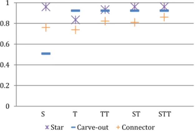
Combinations of several topologies do not considerably increase the coverage for these simple shapes. In contrast, the coverage for complex shapes (star, carve-out, connect-or) is increased by using overlaid topologies. Particularly the combinations of star and tree improve the results. How-ever, even with overlaid topologies, an average of roughly one third of the surface of the carve-out and connector shapes remain uncovered. This is because we simulate arbi-trary placement and rotation on the sensor sheet.
For these complex shapes, we performed a second simula-tion in which we did not require locasimula-tion invariance and rotation invariance, but maintained scale invariance. From a practical perspective this means the user has to adjust the shape at a specific location and rotary angle. The results (Fig. 15) show that in this case even complex shapes are well supported. Even the most complex connector shape yields an average coverage of more than 85% (SD=1.6%). Furthermore, we performed all simulations for topologies with redundant wiring added. This increased the results from 3% to 15%, with most improvement for the tree to-pology.
Technical Experiments
We conducted a series of technical experiments to demon-strate the technical feasibility of the principles. Since our implementation is based on a standard method for capaci-tive sensing, we did not evaluate basic touch sensing in detail, but rather focused on the critical technical aspects that are added by our contributions: we evaluated whether electrodes which fully or partially remain on the cut-out sensor are functional, whether dual-layer sensing is possible and whether the forward error correction can be realized. Figure 16 shows a letter-sized sensor sheet that uses the star topology. It is cut into a user-defined shape (left part within the image). The sensor readings (right part) show that elec-trodes, which remain on the cut-out, are functional and ca-pable of detecting touch input.
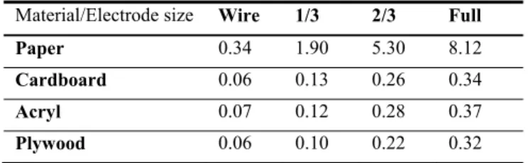
To evaluate the feasibility of cutting in more detail, we test-ed what is the minimum size of a partially cut electrode to Figure 14: Sensing coverage of different shapes using various
topologies. Shapes are freely rotated, translated and scaled on the sensor sheet.
Figure 15: Sensing coverage of complex shapes when placed at one location without rotating, but with scaling.
0 0.1 0.2 0.3 0.4 0.5 0.6 0.7 0.8 0.9 1 0 2 4 6
Triangle Rectangle Ellipse
Star Carve‐out Connector
0 0.2 0.4 0.6 0.8 1
Star Carve‐out Connector S T TT ST STT
Figure 16: Normalized sensor readings of a partially cut sensor sheet.
remain functional with a variety of materials the sensor is sandwiched into (paper, 3mm thick cardboard, 3mm acryl, 3mm plywood). If the electrode gets too small, it is not pos-sible to reliably distinguish whether the user is touching the electrode or touching its wire. Table 1 shows data from electrodes of 2x2cm size, according to the dimensions used in the simulation. The data shows that if only 1/3 of the electrode remains, touch input can still be reliably analyzed. In a third experiment, we studied whether a multi-layer sensor can be cut without creating a short circuit between the two layers. As expected, we were able to validate that the sensor remains functional and both layers independently connect the electrodes with the connector.
Last, we tested the forward error correction principle. Fig-ure 17 shows the data plot for the setup illustrated in Fig. 13a. The data shows that the capacitive measurements of both electrodes roughly add up in the redundant FEC wire. The data demonstrates the feasibility of FEC, but shows that a proper selection of the threshold for sum detection is required, ideally set individually for each electrode. This could be done in the calibration step proposed above. BENEFITS AND LIMITATIONS
Results from the evaluation show that the contributed sen-sor topologies support a variety of standard and more com-plex shapes. Those with a convex shape can be effectively supported by using just one layer with the star topology. They are rotation, location and scale invariant, providing a free-form cutting experience which comes close to cutting conventional, touch-insensitive materials. Overlaid
topolo-gies provide improved support for more complex shapes. Due to the infinite number of possible shapes, our valida-tion can only provide some representative examples to shed light on the space of supported shapes.
We have not addressed how the sensor can cover three-dimensional shapes. This could be done by cutting a 2D shape and folding it to cover the 3D object, or by combin-ing several distinct 2D shapes. We leave this for future work. While the substrate that is used in our prototypical setup is bendable, the printed traces are sensitive to strong bends (i.e. a notch). This can be overcome by using a print technology based on chemical deposition.
Our implementation of a cuttable Letter-sized sensor sheet has a lower number and density of electrodes than used in the simulation and is restricted to two layers. These re-strictions are due to our prototypical manufacturing method. However, the dimensions were sufficient to test and vali-date the electronic properties of the sensor. The simulation results show what can be achieved with higher-density and multi-layer industrial fabrication.
The 1-pin-per electrode design requires more wires than the traditional grid, which raises questions of scalability. This is an inherent trade-off of the design space: either requiring fewer wires which comes at the cost of robustness, or mak-ing it robust to cuts usmak-ing additional wires. In order to alle-viate this issue we propose the following strategies: (1) While current print technologies can already realize wire widths of down to 40nm [6], which allows for a large num-ber of wires on a single layer, wires can also be outsourced to one or more additional layers, using multi-layer printing. (2) Attaching multiplexers at the connector allows signifi-cantly reducing the number of input pins. (3) In a longer-term perspective, printing flexible multiplexers directly on the sensor sheet allows to bundle adjacent wires. Future work should also explore sensors with mixed topologies. These could comprise many smaller areas that are internally wired with the efficient grid design and connected with the controller using our more robust topologies.
Our implementation requires the connector to be located at one specific location on the sheet. Hence, only one shape can be cut out of a sheet. With larger sheets, this possibly wastes large portions of the material. Several spatially dis-tributed access points on the same sheet could be realized by printing multiple layers with displaced topologies. This enables to cut several shapes out of one sheet.
The approach presented in this paper is compatible with a wide variety of non-conductive materials. As first exam-ples, we discussed paper, cardboard, acryl and plywood. For use with transparent materials, the sensor grid could be made transparent using indium tin oxide (ITO).
CONCLUSIONS
In this paper, we contributed principles for a printed multi-touch sensor, which is robust against cuts and removed are-as. The sensor can be embedded within conventional mate-Figure 17: Capacitive sensor readings of a 2+1 redundant
forward error correction block (depicted in Fig. 12a).
Material/Electrode size Wire 1/3 2/3 Full
Paper 0.34 1.90 5.30 8.12
Cardboard 0.06 0.13 0.26 0.34
Acryl 0.07 0.12 0.28 0.37
Plywood 0.06 0.10 0.22 0.32
Table 1: Capacitive sensor readings in pF of partially cut electrodes.
rials and touch-enable them, while maintaining the very direct customization possibilities of the material. The prciples are inspired by topology and coding theory. We in-troduced novel topologies for the circuitry layout of multi-touch sensors that support a variety of cut-out shapes. Fur-thermore, we showed how to increase the set of supported shapes by combining several topologies and by printing a redundancy scheme that realizes a form of forward error correction. We evaluated strengths and limitations of the topologies in a mathematical simulation and presented a first proof-of-concept prototype to demonstrate the possibil-ities for crafting and prototyping.
We consider this first instantiation to be a point of departure for a novel interaction modality with printed electronics: physical cutting and shape adaptation. Future work should address other printed components and devices, including active ones, and show how these can be made robust for desired shape adaptations and against undesired damages. ACKNOWLEDGMENTS
This work has partially been funded by the Cluster of Ex-cellence Multimodal Computing and Interaction within the German Federal Excellence Initiative. We thank Pattie Maes for her valuable feedback and Yoshihiro Kawahara for technical advice.
REFERENCES
1. Arduino Capsense Library.
http://playground.arduino.cc//Main/CapacitiveSensor?from=M ain.CapSense. Accessed: April 2013.
2. Conductive Z Axis Tape. 3M.
http://www.newark.com/3m/9703-25mm-x-33mtr/tape-conductive-z-axis-50micron/dp/95M4936?Ntt=3M+-+9703. Accessed: April 2013.
3. Conductive Inkjet Technology.
http://www.conductiveinkjet.com. Accessed: April 2013. 4. Dietz, P. and Leigh, D. 2001. DiamondTouch: a multi-user
touch technology. Proc. UIST '01, 219-226. 5. Feature size for printed electronics.
http://www.semi.org/en/node/44156. Accessed: April 2013. 6. Fricker, M., Boddy, L. and Bebber, D. Network Organisation
of Mycelial Fungi, 309-330, Springer Berlin Heidelberg. 2007. 7. Hartmann, B., Klemmer, S. R., Bernstein, M., Abdulla L.,
Burr, B., Robinson-Mosher, A., and Gee, J. Reflective physi-cal prototyping through integrated design, test, and analysis.
Proc. UIST '06, 299-308.
8. Holman, D. and Vertegaal, R. TactileTape: low-cost touch sensing on curved surfaces. Proc. UIST '06, 17-18.
9. Hudson, S. E. and Mankoff, J. Rapid construction of function-ing physical interfaces from cardboard, thumbtacks, tin foil and masking tape. Proc. UIST '06, 289-298.
10. Kawahara, Y., Hodges S., Cook B., Zhang, C. Abowd G. In-stant Inkjet Circuits: Lab-based Inkjet Printing to Support Rap-id Prototyping of UbiComp Devices. To appear in
UbiComp'13
11. Liu, S. and Guimbretière, F. FlexAura: a flexible near-surface range sensor. Proc. UIST '12, 327-330.
12. Mistree, B. F.T. and Paradiso, J. A. ChainMail: a configurable multimodal lining to enable sensate surfaces and interactive objects. Proc. TEI '10, 65-72.
13. Mueller, S., Lopes, P. and Baudisch, P. Interactive construc-tion: interactive fabrication of functional mechanical devices.
Proc. UIST '12, 599-606.
14. Paradiso, J.A., Lifton. J., and Broxton, M. Sensate Media - Multimodal Electronic Skins as Dense Sensor Networks. BT Technology Journal, Vol. 22, No. 4, pp. 32-44. 2004. 15. Pérez, G and Paradiso, J.A. B. S.N.A.K.E.: A Dynamically
Reconfigurable Artificial Sensate Skin. B.Sc. Thesis. 2006 16. Qi, J and Buechley, L. Animating paper using shape memory
alloys. Proc. CHI '12, 749-752.
17. Rekimoto, J. SmartSkin: an infrastructure for freehand manip-ulation on interactive surfaces. Proc. CHI '02, 113-120. 18. Rendl C., Greindl, P, Haller, M, Zirkl, M, Stadlober, B, and
Hartmann. PyzoFlex: printed piezoelectric pressure sensing foil. Proc. UIST '12, 509-518.
19. Richardson, B., Leydon, K., Fernstrom, M., and Paradiso, J. A. 2004. Z-Tiles: building blocks for modular, pressure-sensing floorspaces. Proc. CHI '02, 1529-1532.
20. Rosenberg, I., Perlin, K., Hendee, C., Grau, A and Awad N. The UnMousePad: the future of touch sensing. Proc.
SIGGRAPH '09.
21. Savage, V., Zhang, X., and Hartmann, B. 2012. Midas: fabri-cating custom capacitive touch sensors to prototype interactive objects. Proc. UIST '12, 579-588.
22. Song H., Benko, H., Guimbretiere, F., Izadi, S., Cao X., and Hinckley, K. Grips and gestures on a multi-touch pen. Proc.
CHI '11, 1323-1332.
23. Tanenbaum, A. S., Wetherall, D. J. Computer Networks. Pren-tice Hall.
24. Tekscan. F-scan foot pressure mapping system.
http://www.tekscan.com/3001E-pressure-sensor. Accessed: June 2013.
25. Tobjörk, D. and Österbacka, R. Paper Electronics. Adv. Mater. 23: 1935–1961. 2011
26. Todd K. Moon. Error Correction Coding: Mathematical Meth-ods and Algorithms. John Wiley & Sons. 2005
27. Villar, N. and Gellersen, H. A malleable control structure for softwired user interfaces. Proc. TEI '07, 49-56.
28. Villar, N., Izadi, S., Rosenfeld, D., Benko, H., Helmes, J., Westhues, J., Hodges, S., Ofek, E., Butler, A., Cao, X., and Chen, B. Mouse 2.0: multi-touch meets the mouse. Proc. UIST
'09, 33-42.
29. Wiethoff, A., Schneider, H., Rohs M., Butz, A. and Greenberg, S. Sketch-a-TUI: low cost prototyping of tangible interactions using cardboard and conductive ink. Proc. TEI '12, 309-312. 30. Willis K. D.D., Xu, C., Wu, K., Levin, G. and Gross M. D.
Interactive fabrication: new interfaces for digital fabrication.
Proc. TEI '11, 69-72.
31. Wimmer, R and Baudisch, P. Modular and deformable touch-sensitive surfaces based on time domain reflectometry. Proc.