Development of a Scalable Superconducting Memory
by
Brenden A. Butters
Submitted to the Department of Electrical Engineering and Computer
Science
in partial fulfillment of the requirements for the degree of
Master of Science in Electrical Engineering
at the
MASSACHUSETTS INSTITUTE OF TECHNOLOGY
September 2018
Massachusetts Institute of Technology 2018. All rights reserved.
Signature redacted
A u th o r ...
Department of Electrical Engineering and Computer Science
August 31, 2018
Certified by...Signature
redacted
Kafl K. Berggren
Professor of Electrical Engineering and Computer Science
Thesis Supervisor
Signature redacted
A ccepted by
...
Lesli4A.-kolodziejski
Professor of Electrical Engineering and Computer Science
Chair, Department Committee on Graduate Students
MASSACHUSETTS INSTITUTE
OF TECHNOLOGY
OCI
10
2018
MITLibraries
77 Massachusetts Avenue
Cambridge, MA 02139 http://Iibraries.mit.edu/ask
DISCLAIMER NOTICE
Due to the condition of the original material, there are unavoidable
flaws in this reproduction. We have made every effort possible to
provide you with the best copy available.
Thank you.
The images contained in this document are of the
best quality available.
Development of a Scalable Superconducting Memory
by
Brenden A. Butters
Submitted to the Department of Electrical Engineering and Computer Science on August 31, 2018, in partial fulfillment of the
requirements for the degree of Master of Science in Electrical Engineering
Abstract
Superconducting computers promise very high computation speeds while also con-suming far less power than their conventional counterparts. However, much of the progress in this field has been stymied by the lack of a scalable superconducting mem-ory technology. In this thesis, I present the design of, and demonstrate the operation of, a superconducting nanowire-based memory cell. In contrast to existing designs, this cell operates by means of kinetic rather than geometric inductance. Thus, the cell size can be made much smaller than would otherwise be possible. With the suc-cessful operation of the single cell, paths to larger arrays are explored, and a small array demonstrated. The further development of the technology demonstrated in this work will allow for the production of large-scale superconducting processors, and the eventual development of superconducting supercomputers.
Thesis Supervisor: Karl K. Berggren
Acknowledgments
Much of the work presented in this thesis would not be possible without the efforts of many of my colleagues. I would like to acknowledge:
My advisor, Prof. Karl Berggren, for his insights, his encouragement, and his
dedication to the development of his students. His enthusiasm for our work really
kept the project going - even when everything seemed to be going wrong.
Adam McCaughan, for his development of the nanocryotron devices, used exten-sively in this work, and for his initial efforts towards the superconducting memory project.
Qing-Yuan Zhao, for his contribution towards the non-destructive memory covered in chapter 2, and for the fabrication of the devices covered in chapters 2 and 3.
Reza Baghdadi, for the contributions towards, and fabrication of, the devices presented in chapter 4.
Emily Toomey, for her helpful discussions, and extensive experimental assistance. Murat Onen, for his help with simulating designs, and experimental assistance. Dorothy Fleischer, for helping keep me organized, and for her ever-helpful attitude and generosity.
Di Zhu, Marco Colangelo, and Andrew Dane, for their input, collaborations, and experimental assistance.
The work that I conducted in pursuit of this thesis, and other in other related projects, was only made possible by the support and advice that I received from my family, and friends. In particular, I would like to thank:
Dr. Raad Raad, for supporting my research, for all his help and encouragement, and for the many hours of discussions we have had over the years. Without his influence I would likely not have made it to where I am today.
Tony and Joe - truly the best MIT has to offer.
Finally, I would particularly like to thank my parents for their unwavering support and dedication. I am forever grateful for the sacrifices that they have made in order for me to pursue the path that has lead to this thesis being written.
Contents
1 Introduction
1.1 Superconductivity and superconducting circuit components
1.1.1 Josephson junctions . . . .
1.1.2 Superconducting nanowires . . . .
1.1.3 Kinetic inductance in nanowires . . . . .
1.1.4 Circuit model of superconductivity . . .
1.1.5 The cryotron . . . .
1.2 Superconducting nanowire devices . . . .
1.2.1 Constriction . . . .
1.2.2 nTron . . . .
1.2.3 hTron . . . .
1.2.4 yTron . . . .
1.3 Superconducting memories . . . .
1.3.1 Need for a cryogenic-compatible memory
1.3.2 Existing memory technologies . . . .
1.4 Thesis goal . . . .
1.5 Thesis outline . . . .
2 Non-destructive readout memory
2.1 Memory approach . . . .
2.2 NDRO cell operating principals . . .
2.2.1 Writing to the memory . . . .
2.2.2 Reading from the memory . .
47 47 . . . . 48 . . . . 51 . . . . 52 . . . . 53 . . . . 54 . . . . 56 . . . . 57 . . . . 59 . . . . 62 . . . . 65 . . . . 67 . . . . 68 . . . . 68 . . . . 69 70 73 . . . . 74 . . . . 77 . . . . 78 . . . . 8 0
2.2.3 Cell design limitations and trade-offs . . . . .
2.2.4 Cell layout . . . .
2.3 Cell simulation . . . .
2.4 Basic NDRO cell measurements . . . .
2.4.1 General immersion measurement procedure . .
2.4.2 Initial NDRO measurement setup . . . .
2.4.3 IV Curves . . . .
2.4.4 Experimental setup . . . .
2.4.5 Memory operation results . . . .
2.5 Revised design . . . . 2.5.1 Revised cell design . . . .
2.5.2 Low error rate measurement setup . . . . 2.5.3 Experimental results . . . .
3 NDRO array design
3.1 Array architecture . . . .
3.1.1 Resistively isolated design . . . .
3.1.2 Multiplexed column design . . . .
3.1.3 Array design size and power comparison . . .
3.2 Multiplexer design . . . .
3.2.1 Multiplexer operation . . . .
3.2.2 Superconducting multiplexer implementation .
3.2.3 Prototype multiplexer testing . . . .
4 Destructive readout cell and array design
4.1 Operating principal of the DRO cell . . . .
4.1.1 Writing to the memory . . . .
4.1.2 Reading from the memory . . . .
4.1.3 Cell design limitations and trade-offs . . . . .
4.1.4 Cell simulations . . . . 4.1.5 Cell layout . . . . . . . . 82 . . . . 85 . . . . 87 . . . . 92 . . . . 93 . . . . 96 . . . . 96 . . . . 100 . . . . 105 . .. . . 111 . .. . . 111 . . . . 113 . . . . 115 119 119 120 126 128 132 133 135 137 143 . . . . 144 . . . . 145 . . . . 146 . . . . 147 . . . . 149 . . . . 152
4.2 Multilayer hTron . . . .
4.2.1 D esign . . . .
4.2.2 Experimental results . . . .
4.3 DRO array design . . . .
4.3.1 Array design . . . .
4.3.2 Array simulations . . . .
4.4 Testing the initial DRO array design . . . .
4.4.1 Initial cell experiments . . . .
4.4.2 Debugging design - magnetic modulation of cell switching
4.5 Design revision . . . .
4.5.1 Automated array testing . . . .
4.5.2 Isolated unselected cell testing . . . .
4.5.3 hTron distributions in helium immersion measurements .
4.6 Refined test procedure and experimental results . . . .
. . . 154 . . . 154 . . . 156 . . . 158 . . . 159 . . . 161 . . . 163 . . . 163 current 167 . . . 170 172 175 . . . 177 . . . 179 5 Experimental setup and apparatus design
5.1 Automated testing . . . . 5.1.1 Integrated optimizer . . . .
5.1.2 Cost function . . . .
5.2 Design and construction of cryogen-free magnetic-modulation
experi-mental apparatus . . . .
5.2.1 Overview of design . . . .
5.2.2 Sample mount . . . .
5.2.3 Thermally insulated standoffs . . . .
6 Conclusion and future work
187 188 189 192 199 200 204 206 211
List of Figures
1-1 Schematic showing the basic structure of a Josephson junction. The
distance between the two superconducting materials must be very small in order for tunneling to occur. When an insulator is used to separate the superconductors the junction is referred to as a SIS junction. It is also possible to use a normal metal, in place of the insulator, to crease a SNS junction, it is even possible to use a weaker superconductor to
form a SsS junction. . . . . 49
1-2 Current-voltage relation of a typical Josephson junction. The junction
can pass a current with no voltage drop provided the current is less
than the critical current Ic. When the critical current is exceeded
the junction switches operating mode and presents a voltage 2A/e
where A is the superconducting gap, and e is the elementary charge.
If the current is increased the junction behaved as a resistor. Upon decreasing the current, when close to zero the junction will return to a zero voltage drop. Note that the IV curve is rotationally symmetric,
1-3 Schematic drawing of a typical cryotron used by Buck. The device con-sists of a 00.009" uncoated tantalum gate wire wrapped with around
250 turns of a 00.003" insulated niobium control wire. When a
cur-rent Ic is applied to the control wire, a magnetic field is induced in the solenoid. This field suppresses superconductivity in the gate wire. As Ic is increased, the gate current Ig that the wire can support with-out transitioning to the normal region will progressively decrease. A greater suppression of superconductivity occurs in the gate wire than
the control wire owing to the gate having a lower Tc, and lower B,. . 54
1-4 Schematic symbol for a cryotron, as proposed by Buck. This symbol
is derived from the structure of the cryotron with the control wire depicted as a coil around a thicker conductor, that being the gate. Additionally, the symbol graphically demonstrates that the cryotron does not behave differently if the currents Ic and/or Ig are reversed in
direction, as only their magnitudes is of importance. . . . . 55
1-5 Schematic symbol for a superconducting nanowire constriction (a), and
a sketch of the layout of a constriction (b). There is no generally
accepted symbol for a nanowire, we will use this symbol throughout this work. The constriction shown in (b) has been switched to the "normal" state. While the vast majority of the wire is still superconducting,
there exists a hotspot at the narrowest region of the wire - where the
current density is the highest. As a current I is being applied to the constriction, a voltage V will be dropped across the normal region. The magnitude of the current I can cause the hotspot to grow or shrink. If the bias I is lowered sufficiently then the hotspot will vanish and the constriction return to the superconducting state. The jog lines indicate
1-6 Sketch of the current-voltage relation for a single current-biased su-perconducting constriction. The constriction can carry any current without developing a voltage, provided that the magnitude of the cur-rent is less than the critical curcur-rent Ic. If Ic is exceeded, then the device will enter the resistive state. Once in the resistive state, the device behaves similar to a resistor. From the resistive state, if the current is lowered to below the retrapping current Ir, then the device will return to the superconducting state. Note that the IV curve is ro-tationally symmetric, and that switching and retrapping only depends
on the magnitude of the current . . . . 59
1-7 Schematic symbol for the nTron (a), and a sketch of a typical nTron
layout (b). In the absence of a gate current Ig, a high channel current
I, can be sustained without the device switching and a channel voltage
V forming. However, in the presence of a sufficient gate current, a hotspot will form at the gate. This hotspot reduces the effective width of the channel and increases the local temperature, thus leading to a reduction in the magnitude of current Ic that can be sustained without the channel switching. The narrowest region of the channel is located to one side of the gate such that during retrapping, the gate will become superconducting prior to the channel. The symbol for the device was designed such that it depicts which side of the narrow region of the
1-8 Sketch of a typical nTron suppression curve. The switching current of the channel I,,, is a function of the gate current Ig. The switching current of the channel is largely unaffected by the gate current while the gate is superconducting. That is, when the gate current is less than its
critical value c,g and no hot spot has formed, there is little modulation
of the channel switching current by the gate current. Once the gate switches, and a hotspot forms, the channel is rapidly suppressed by the gate current. This rapid suppression leads to an operating region in which the nTron possesses a very high gain. This effect begins to
diminish with the application of increasing gate current. . . . . 61
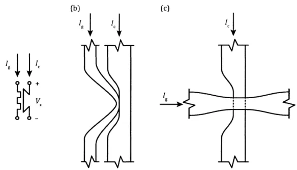
1-9 The schematic symbol (a) for the hTron, a sketch of an in-plane hTron
layout (b), and a sketch of the layout for a multilayer, or stacked, hTron (c). The in-plane hTron is typically constructed from the same
superconducting film. This allows the gate to be located relatively
close to the channel - within 100 nm. The multilayer hTron can be
fabricated with either a normal or superconducting gate. The gate can be within 30 nm of the channel as it is only separated by a dielectric layer. For the in-plane hTron the geometry of the channel and gate are limited by the need to keep them in close proximity, while also avoiding current crowding in the channel. For the multilayer hTron design, the channel and gate can have almost any geometry required, provided
there is some location where they overlap - or at last come close to
each other. While many different geometries are possible, typically,
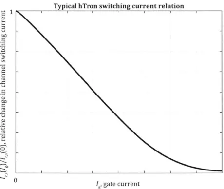
1-10 Sketch of a typical suppression curve of a hTron with a normal metal
heater. As increasing gate current Ig is applied to the device, the
channel switching current Jc,s(Ig) decreases. After some gate current a
regime of diminishing returns is entered where the higher gate currents are required to achieve greater suppression. In most devices normal metal gate hTrons that have been tested experimentally, it takes an very large gate current to totally suppress superconductivity, if it is ever achieved. On the other hand, superconducting gate hTrons can relatively easily achieve total suppression of the gate; however, a similar region of diminishing returns is witnessed. With a superconducting gate, there is a region of zero suppression from Ig = 0 to Ig = Ic,g, the
gate critical current, in a similar manner to that of the nTron - see
figure 1-8. ... ... 64
1-11 Schematic symbol for a yTron (a), and a sketch of a typical yTron
layout. The sense current I, is the current to be measured
non-destructively. If the yTron is operated correctly, this current should never be interrupted. The sense current is determined by applying a
bias current Ib while monitoring the bias voltage V. With a low sense
current, a relatively low bias current is required to switch the bias port, due to the high current crowding that occurs on the yTron corner. On the other hand, when a high positive sense current is applied, the bias current that is required to switch the bias port is comparatively higher than in the low bias case. This increase in switching current is due to the decreased current crowding that occurs when the biases applied to
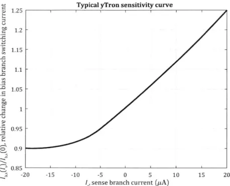
1-12 Sketch of the sensitivity curve of a typical yTron. This sketch is adapted from experiential results. In contrast to the other nanowire devices presented here, the switching current of the yTron increases
with the increased application of an external current - the sense
cur-rent. This effect will only occur over a region where the sense arm has not switched. Once the sense arm switches, then the yTron begins to behave as an nTron. While the sense arm is superconducting, we have that the bias arm switching current Ims(Is) increases with increasing sense current I. With the application of a negative sense branch cur-rent, the switching current can be seen to decrease, but only to around
90% of its zero-bias value. The yTron is intended to operate with
pos-itive I,. The sensitivity curve of the yTron is injective, and thus allows for the sense current to be measured without disrupting the supercurrent. 67
2-1 Schematic demonstrating how the IV curve of a hysteric nanowire can
be exploited to implement a poor memory. Here, the wire is biased to
Ib = 0.6Ic. At this bias, the load-line intersects the IV curve of the
wire at two locations, thus there are two possible states, both of which happen to be stable. To switch between these two states a current pulse is applied. A positive pulse greater than 0.4Ic is applied to set the memory into the "1" state. A negative pulse greater than 0.4cI is applied to reset the memory to the superconducting "0" state. When in
the "1" state, the cell dissipates 0.36I Rh continuously, where Rh is the
hot spot resistance (which is on the order of 200 Q to 1000 Q for NbN). For typical values, the power dissipation of such a memory can be esti-mated to be around 0.25 piW when in the "1" state. Hence, a memory constructed this way would not be acceptable in many superconducting
2-2 Derivation of a superconducting dual of a CMOS DRAM cell. (a) a typical DRAM cell as implemented in CMOS; (b) a simplified model of the CMOS DRAM cell where the enhancement mode MOSFET has been replaced by a normally open switch; (c) the dual of the simplified circuit, note that the switch is now normally closed. The capacitor voltage V, which previously held the state of the cell is now a persistent current Ip, the magnitude and/or sign of which can now be used to store the state of the cell; (d) a nanowire implementation of the dual circuit
where the normally closed switch has been replaced with a hTron. . . 76
2-3 Simplified schematic of a basic NDRO cell. The device has three ports,
namely a write enable, a write port, and a read port. The loop which carries the persistent current Ip, consists of the channel of the hTron,
the yTron, and the two inductors LL and LR where LL < LR. The
write enable port is galvanically isolated from the loop. . . . . 77
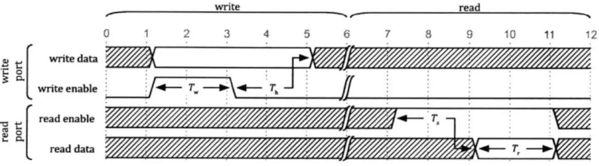
2-4 Timing diagram for writing to, and reading from, a NDRO memory cell. This diagram summarizes the logical sequence of accessing the memory. The levels of current and their signs will depend on the exact
cell design and operating mode. . . . . 79
2-5 Sketch of a typical yTron sensitivity curve based on experimental
re-sults, that has been annotated to show the operation of the yTron memory readout. When the yTron is used to read the loop current, we have the sense current is the loop current, Is = Ip. In this example, the yTron is biased at I, = 1.09Ib,S(O), that is 9% over the zero bias switching current of the yTron. At this point we have the correspond-ing loop current Ip,th is approximately mid-way between the "0" state loop current and the "1" state loop current. Thus, the yTron voltage V will be zero if the memory is in the "1" state, since the loop current will be Ib,s(Ip) > [r. Conversely, if the memory is in the "0" state, then
the loop current will be low and Ibs,(Ip) < r, so the read bias will be
2-6 Layout of a compact NDRO cell used in the first set of measurements. The design shown is the exact layout of the device tested in section 2.4. The black area indicates where NbN has been etched away (leaving the bare substrate below), and the white area is where NbN remains. The drawing is shown this way because a positive tone resist was used, so the black area is where the resist was exposed. The jog lines indicate leads that extent to connection pads. Note, the hTron and yTron have
been highlighted by a dashed box around each device. . . . . 85
2-7 Schematic used in the LTspice simulation of the NDRO cell. Note the
inclusion of the two resistors R1 and R2 which are not physical, but are
included so that LTspice will reliably converge. This approximation is
valid for small values of these resistors and for short time scales. . . . 88
2-8 Results of a simple LTspice simulation of a single NDRO cell operated
in the pulse readout modus. In this simulation, the cell is set (placed
in the "1" state) at 50 ns. At this time, the loop current I, can be
seen to increase - indicating that the write was successful. The cell is
then read at 100 ns. During the read, the yTron does not switch, as expected when the cell is set. The cell cleared (placed in the "0" state) at 150 ns. Again, the loop current can be seen to respond accordingly
by reducing to zero. Finally, at 200 ns the memory is read again, but
this time the yTron switches. The switching of the yTron indicates that the read was successful, and that, at least in this simulation, the memory is working as expected. Note that the loop current can be seen here to be decaying. This decay is an artifact of the simulation,
specifically the resistors R1, and R2. In reality there is no decay in the
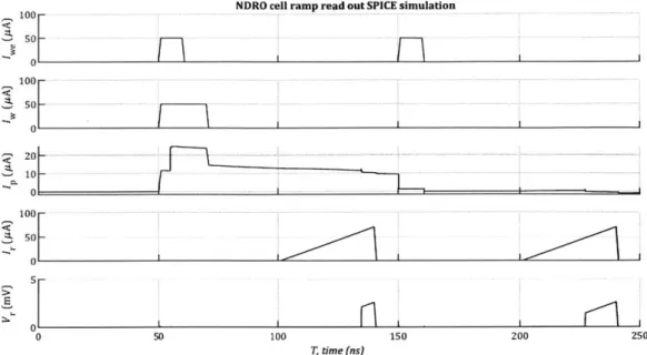
2-9 Results of a simple LTspice simulation of a single NDRO cell operated in the ramp readout modus. The write portions of this simulation are identical to those used in figure 2-8. The ramped readout current can be seen to show the switching current of the read port being modulated
by the persistent current Ip. When the cell is in the "1" state with a
high persistent current, the read port switching current can be seen to be higher than when the cell is in the "0" state with a zero persistent
current. . . . . 91
2-10 Results from an IV curve measurement made on the three ports of an NDRO cell. The figures on the left shows the time domain traces of the bias voltage and the device voltage. Note that a bias resistor of 10 kQ was used. The figures on the right show the IV curve of the device. Each of these experiments was conducted with all unused ports terminated into 50 Q. Note that in these plots the data has been
decimated by a factor of 100. . . . . 97
2-11 Depiction of the theorized hotspot growth in two different nanowire geometries. Both nanowires are exposed to a monotonically increasing current I. This current eventually leads to the switching of the single constriction in (a) and the first constriction in (b). As the current con-tinues to increase, the hotspots will grow in the directions indicated by the gray arrows. In (a), the IV curve will not exhibit any steps other than the first switching event; however, due to the non-constant cross section of the nanowire, the IV curve will depict a curve. In (b), the IV curve will be similar to (a) at first, as the hot spot continues to grow. At some point however, the current density at the second con-struction will cause superconductivity to breakdown at this location, and a second hotspot will form. The formation of this second hotspot will result in a second step in the IV curve (separate from the first constriction switching). Thus, we can see how the non-constant width
2-12 Schematic of the NDRO cell write and ramp readout scheme. This figure features two write/read cycles. The first operation, at 50ns, is a set operation. Note that the channel bias is applied held after the deassertion of the write enable. The yTron switching current is them measured by applying a ramp to the read port. At some point the yTron switches and a voltage is seen at the read port. The time delay between the start of the write operation and the switching of the yTron is used to determine the current required to switch the yTron. At 200 ns the memory is cleared, for the unipolar wire scheme, the write bias is set to zero for this operation, and for the bipolar write scheme, the write bias is a negative pulse (the inverse of the set pulse shape). Again the memory is read out by applying a ramping current to the yTron. After a clear the switching current of the yTron should
be lower than after a set, so we expect the skew times T,O < Ts,1.
The time until the device switches is used as the oscilloscope has more time resolution than voltage resolution, and so a better estimate of the
switching current can be obtained by this method. . . . . 101
2-13 Experimental setup for basic NDRO measurements. AWG1 was used
to control the write operation. AWG2 is triggered by AWG1, and after some delay, initiates the read operation. In order to minimize reflections, and enable high-speed operation, a system impedance of Zo = 50 Q was used. As the devices required relatively small currents
to operate, attenuators were used to reduce signal amplitudes. To
2-14 Switching probability density estimations, using a unipolar write pulse consisting of a positive write current for the set signal, and a zero write current for the reset signal. The horizontal axis represents the voltage bias that, through the bias network, resulted in a sufficient current to switch the yTron. The solid and dashed lines show a maximum likelihood fit of a Burr distribution to each histogram. The insert is a magnified section of the plot showing the overlap between the two distributions. It can be seen that, while the memory operates very
well, there are a number of errors. . . . . 106
2-15 Switching probability density estimations, using a bipolar write pulse
of a positive write current for the set signal, and a negative current pulse for the reset signal. The horizontal axis represents the voltage bias that, through the bias network, resulted in a sufficient current to switch the yTron. The solid and dashed lines show a maximum likelihood fit of a Burr distribution to each histogram. The insert is a magnified section of the plot showing the overlap between the two distributions. It can be seen that there were no errors observed, and that the overlap between the tails of the fits are very small, thus
resulting in a very low fit-estimated error rate. . . . . 109
2-16 Extrapolated readout operating margins for both the unipolar and
bipolar operation of the cell. These results were found using the fits shown in figures 2-14 and 2-15. The vertical axis indicated the relative tolerance in the yTron readout current. The horizontal axis provides an upper bound on the error rate. Examination of this graph allows for the determination of the readout operating margin for a desired upper
2-17 Layout for the revised NDRO cell used in the low error rate
measure-ments. The design shown is the exact layout of the device that was tested in the following section. The black area indicates where NbN has been etched away (leaving the bare substrate below), the white area is where NbN remains. The jog lines indicate leads that extend to the connection pads. Note the hTron and yTron have been highlighted
by a dashed line around each device. This layout can be seen to be a
stretched version of the original layout shown in figure 2-6. Two ad-ditional changes were made. First, the ground connection was made narrower than the cell, and shifted below the hTron channel so as the
further increase LR. Second, the design of the hTron was modified in
an attempt to reduce the hotspot size. . . . . 112
2-18 Experimental setup for the final, low BER NDRO cell measurements. A known PRBS is generated by AWG1 and used to trigger AWG2
which provides the write bias. The second channel of AWG1 provides the write enable signal. AWG3 is synchronized to AWG1, and provides the read bias pulse, which is swept during the experiment. A counter is used to track the number of writes, and the number of zeros read from the cell. From the counter's results, the error rate can be estimated since we know the intended number of zeros written. To reduce reflec-tions 50 Q series termination resistors were added close to the sample
on the sample PCB. . . . . 114
2-19 Results of the BERT on the revised cell. Each point represents one
experiment at one read bias level. At each point, at least 3 x 10⁵
write/read operations were performed. Two fits were added to the plot, one for the tail of the write-one-read-zero (WIRO) error and the other for the tail of the write-zero-read-one (WORI) errors. The intersection
of these fits predicts an ultimate error rate around PEmin ~ 10-1.
However, these fits lines are relatively, steep which means that the
3-1 Schematic of a resistively isolated NDRO cell. The additional hTron is normally shorting the yTron port to ground. This prevents the write current I, from being seen by the yTron, and so allows the read port to be common to all cells in the column. The two resistors prevent
parasitic supercurrent paths from forming. . . . . 120
3-2 Timing diagram showing the two types of timing-limited read
opera-tions. On the left is a read-bias-setup-time Ts,b limited operation, and
on the right is a read-enable-setup-time Tsre limited operation. It can be seen that in both cases, there is a setup time between the appli-cation of the bias and the data becoming valid T,,b, and between the application of the read enable signals and the data becoming valid Ts,re. It should be noted that regardless of the order in which the enable and
the bias signals are applied, both setup times must be satisfied. . . . 122
3-3 Schematic showing the connections between resistively isolated NDRO
cells to form an m-bit word, n-row bank. In this figure the use of resistive hTron gates is assumed (provided bit-access is desired), if superconducting gates are used then series resistors are required. It can be seen that forming an array from the resistively isolated cells involves the hTron gates being connected in cross-bar arrangements, read ports connected in parallel along columns, and cell write ports
3-4 Timing diagram for word-access write and read to the NDRO cell array of either the resistively isolated or multiplexed design. The signal labels in this figure reference buses, specifically WEc is a bus formed by the column write enable lines, WEr is the row write enable lines, W is the write signals, OE, is the column output enable lines, OEr is the row output enable lines, and finally R is the read lines. For the word access scheme, the column lines, both write and read enables, are all grounded; alternatively, these could be held at a high potential and active-low row signals could be used. The first step in order to perform a write is to assert the desired rows write enable signal. The selection of the desired row is equivalent setting WEr to be the one-hot address of the desired cell. Upon the falling edge of the write enable signal, the write data must be valid. That is, the data to be written to that row must be present at the W port. Once the write enable signal has been deasserted, the write port can be set arbitrarily. For a read operation, the desired row is selected by asserting the corresponding output enable signal. This operation is equivalent to setting the OE, to the one-hot address of the desired row. The read bias current is also applied to the read port. The output enable and read bias signals can be applied in
any order, or simultaneously - as shown here. The read port will then
present the result of the read asynchronously. The presented output will be the complement value stored at the selected address. The data will be held, and is valid, for as long as the output enable and read bias is maintained. When the read is complete the biases are simply
3-5 Timing diagram demonstrating the bit-access applied to a NDRO ar-ray of either the resistively isolated or multiplexed design. This timing diagram shows both write and read accesses to a 2 x 2 array, although the operation could be extended to an array of any size. This dia-gram shows four writes and four reads, one to each cell of the array. In order to achieve bit-access, tri-state write enable and/or column enable drivers are required (depending on if bit-access is only needed for writes, reads or both). A write operation to a single cell requires a current to be passed through that cell's write enable hTron gate. This can be achieved by the WE column and row drivers presenting a high impedance to all lines other than those corresponding to the desired cell. For the lines corresponding to the desired cell, one line, say the column signal, must be high, and the other, say the row, must be low. With the write enable signals set, the data to be written to the selected cell is applied to the corresponding column write port. Other columns can have any signals applied as they are not selected. The selected write enable lines are then either returned to the high impedance state, or all set to the same level. Once this is complete, the write bias can be removed, and the write operation is complete.
A read operation is conducted in a similar manner. One of either the
column or row output enable signals that corresponds to the selected cell is set high, and the other set low. The read bias is then applied to the read port corresponding to the column in which the desired cell resides. The voltage of this port can then be measured to determine the state of the cell. Like in the word-access scheme, the read voltage
3-6 Schematic showing the connections between NDRO cells and hTron multiplexers to form an m-bit word, n-row bank. The bold lines indi-cate buses. In this array, the write enable heaters and write ports are connected in the same manner as that shown in figure 3-3, for the resis-tively isolated design. Here, the read ports of each cell are connected to multiplexers, which allow read access to the cells. As the multiplexers are constructed with nanowire devices, when no cell is selected, all read ports within a column will be shorted together. Thus, to prevent par-asitic loops from forming through the multiplexer, a bank of resistors
is placed at the input to each multiplexer. . . . . 127
3-7 Comparison of the effective cell size for both a resistively isolated and a
multiplexed column design. The relative size is computed with respect to the area of a single cell that contains a single hTron. Note that for this calculation, a word with of 32-bits was assumed. It can be seen that the resistively isolated array has a constant size of four times that of the single cell. In contrast, the multiplexed design starts the same size as a single cell for a bank containing one row, and grows as the bank size grows. The multiplexed design asymptotically approaches the limit of 3 + 1/m = 3.03125 for an array of infinite size. Thus, the multiplexed array is always smaller than the resistively isolated array
3-8 Comparison of the power dissipated during a read operation by the cell selection circuitry for both a resistively isolated and a multiplexed column array. Note that for this calculation, a word with of 32-bits was assumed, further it was assumed that the entire word was read, and that an equal number of bits were zero and one. For small bank sizes, the multiplex column and resistively isolated designs perform comparably. However, as bank size grows, the resistively isolated de-sign's power dissipation grows as a square of bank size, whereas the multiplexed column design grows logarithmically. Thus, for large ar-rays the multiplex column design vastly out-performs the resistively
isolated design for read power dissipation. . . . . 132
3-9 The logic that governs a typical four-to-one digital multiplexer. The
schematic has been broken into two sections, with one being a two-input decoder, and the other being a four-to-one one-hot multiplexer. In this case, the select inputs to the multiplexer must be one-hot signal, and this requirement satisfied by the output of the decoder. Porting this design into nanowire devices would yield a very poorly performing
device, for this reason an adaptation of this design is used instead. . . 134
3-10 Schematic of a possible implementation of a four-to-one analog
mul-tiplexer. The parts of the circuit that are common between a digital and analog multiplexer were drawn in gray. In this analog variant of the multiplexer, the AND-gates are replaced with analog switches, and the OR-gate with a connection between all the switch outputs. For an
analog multiplexer such as this, the output port "0" is also referred to
3-11 A four-to-one, one-hot multiplexer constructed with as a hTron tree. The schematic of the multiplexer is shown in (a), and the correspond-ing circuit symbol of the device is shown in (b). When enabled, the multiplexer allows for one of the four inputs to be connected to the common port (0) by apply a bias to the select line (Sx) with the same subscript as the desired input (Ix). The hTron tree multiplexer's gate arrangement is designed to ensure that no matter which input is se-lected, only one hTron per state is on. For example, in this design, no matter which of the input is selected, only two hTron will be on at any
one tim e . . . . . 138
3-12 Layout of the prototype two-to-one hTron multiplexer. The design shown is the exact layout of the device tested in this section. The black area indicates where NbN has been etched away (leaving the bare substrate below), and the white area is where NbN remains. The jog lines indicate leads that extent to connection pads. While this design is only a two-to-one multiplexer, with the third hTron it becomes one half of the four-to-one multiplexer shown in figure 3-11. One side of
each heater is connected to ground. . . . . 139
3-13 Schematic drawing of the experimental setup used to test the hTron
multiplexer. A bias resistance of Rb = 10 kQ was used for the
experi-ments. The current through the common port 'com was determined by
the voltage drop across the bias resistor Rb. A gate bias Vgx was only applied to the input port which was grounded. In this manner, the common port should remain connected to the unselected port, which was monitored by the oscilloscope, while the IV curve of the grounded port was tested. If we see typical hTron IV curves, without the channel through which we are monitoring the voltage, switching, then we can
3-14 Operation of the prototype superconducting two-to-one multiplexer. These results have been decimated by a factor of 50. In (a), input two is grounded, and the voltage at input one is monitored for different
voltages Vg,2. In (b), input one is grounded, and the voltage at input
two is monitored for different voltages Vg,1. It can be seen that the
operation of both hTrons is nearly identical, and that the multiplexer is operating as expected. The port from which we are monitoring the voltage is not switching, and the gate is successfully suppressing the
opposing hTron. . . . . 141
4-1 Schematic of the DRO cell. This cell design is similar to the NDRO
cell design withe the only major difference being that the yTron has been replaced with a second hTron. The cell is selected by applying
a current I, to the enable port. The cell is intended to be written
to by a bipolar current applied to the channel Ic, which results in a
persistent current I_, being induced in the loop. Readout is achieved
by measuring the switching current of the channel by applying a high
current to Ic, and monitoring the resultant voltage. . . . . 144
4-2 Schematic used in the LTspice simulation of the DRO cell. Note the
in-clusion of the two resistors R1 = R = I pQ which are not physical but
are included so that LTspice will reliably converge. This approximation
4-3 Results of a LTspice simulation of a single DRO cell operated in the pulse readout modus and using the write enable signal. In this simula-tion, the cell is set (placed in the "1" state) at 10 ns. At this time the,
loop current Ip can be seen to increase - indicating that the write was
successful. The cell is then read at 30 ns. During the read, the memory
does not switch - as expected when the cell is set. The cell is cleared
(placed in the "0" state) at 50 ns. Again, the loop current can be seen
to respond accordingly - reducing to a negative value. Finally, at 70 ns
the memory is read again, but this time the memory switches. The switching of the loop, and the corresponding production of a voltage V, during a read "0", and the lack thereof for a read "1" indicate that, at least in this simulation, the memory is working as expected. In this
figure, the values IL and IR, are the currents through the channels of
the left and right hTron constructions, respectively. . . . . 151
4-4 Layout of the first single DRO cell. The black area indicates where
NbN has been etched away (leaving the bare substrate below), and the
white area is where NbN remains. The gray area indicates the location where resist will be exposed and developed such that an oxide and metal can be evaporated and later lifted off to form the heater. The
jog lines indicate leads that extent to the connection pads. . . . . 152
4-5 IV curve of one of the first working hTron device conducted at three
gate voltage biases. The experimental data was moving-average filtered prior to being decimated by a factor of 25 in preparation for this figure.
It can be seen in the Vg = 0 V curve that the switching and retrapping
currents are very close together, within around 20%. Typically, the retrapping current is around 20% of the switching current. Thus, this figure here suggests that, even without the application of a current to the gate, the channel is suppressed substantially. With increasing gate bias voltage, an increase in the suppression is seen. With ultimately
4-6 IV curve of a multilayer hTron with the application of three different gate voltage biases. The experimental data was moving-average fil-tered prior to being decimated by a factor of 25 in preparation for this
figure. It can be seen in the Vg = 0 V curve that the switching and
retrapping currents are quite distinct from each other and are in line with those obtained in previous experiments on contributions. With
the application of a gate bias of Vg = 0.45V the switching current of
the device can be seen to reduce - while the retrapping behavior is
unchanged. With the increased application of gate bias, the switching current is suppressed further until the device becomes non-hysteretic,
and the switching and retrapping current merge. . . . . 157
4-7 Layout for the first DRO array. This array features four DRO cells of
the same design as that presented in section 4.1.5, which have been arranged into a 2 x 2 configuration. The word size for this memory is 2 b, and there are two rows in the bank. It can be seen that the cell design shown in figure 4-4 was simply repeated four times with the terminals connected to form the desired array. A large space was placed between the cells to ensure that in initial tests there was no inter-cell
interference - later tests showed that this space is unnecessary, and that
cell heating is highly localized. On the extremes of the heater lines, the connections to the pads were made wide so as to reduce the resistance, and hence power dissipation, in the interconnects. Additionally, the connections from the heaters to the pads were made to be equal in length, so that their resistances would be equal, and as a result the
4-8 Simulation of a DRO cell within an array. This simulation demon-strates that the state of the cell is unaffected by operations accessing other cells in the array. First, the cell in question is written into the "1" state. Then other cells in the array written to the "0" state, written to the "1" state, and read out. None of the operations performed on the other cells in the array caused the cell in question state's to change, as witnessed by the persistent current I remaining unchanged, and the read operation indicating that the cell is in the "1" state. The same test is then performed again with the cell instead being written into the "0" sate. Again, the state of the cell was unaffected by accessed to other cells in the array, and the subsequent read provided the correct
result. . . . . 162
4-9 Experimental setup for the DRO single-cell measurements. This setup can be used for ramp and pulse-based readouts; however, here we focus on the pulse-based readout scheme. Since the experiments utilize rel-atively fast pulses, a system impedance of 50 Q was used for the setup including the AWG outputs and oscilloscope input. In order to moni-tor the cell voltage, a splitter was used to divide the cell bias between the device and the oscilloscope. The downside of this approach is that the oscilloscope sees the cell's voltage response superimposed on the cell's bias. Additionally, the heater signal was split between the device and the oscilloscope. This allowed for the tuning of the timing of the
4-10 Oscilloscope traces of the signals applied to, and read from, the DRO cell. The channel bias is the signal that was generated by the AWG. Channel voltage is the combination of the signal applied to the cell
and the reflections from the cell - see figure 4-9. Finally, the heater
voltage trace is the signal applied to the heater. The markers on the channel voltage plot show where the voltage is sampled to determine if the device switched. The first pulse sets the cell into the "1" state. Following a short pause, the state of the cell is read out. The voltage is sampled at the first arrow. This voltage is below some threshold
voltage Vh. After another pause, the cell is then cleared to the "0"
state. Again, the cell is read out using the identical read pulse to that used in the first read. This second read resulted in the cell switching,
and the resultant voltage pulse is above our threshold voltage Vt h,
thus indicating a "0" read. The threshold voltage is Vth determined
experimentally, and chosen to give the best error rate. . . . . 165
4-11 Probability density of the read pulse amplitude for reads that occurred after a "0" was written (negative write) and after a "1" was written (positive write). The horizontal axis in this plot corresponds to the amplitude of the two markers shown in figure 4-10, and should not be confused with the switching current. This figure is composed of 10, 000 write/read cycles, each of which alternated between writing a "1" and writing a "0". The results are divided into two by a threshold voltage Vth. Any sample whose read voltage was below th is determined to be
a read that resulted in a "1", and those above the threshold a read that
resulted in a "1". The threshold was chosen to be Vth = 5 mV since this
4-12 Setup used to test the magnetic modulation of the DRO cell's switching current. In this setup, the memory chip was placed in close proximity to a custom-made superconducting magnet. The leads of the magnet were attached to copper wires within the LHe. The ground for the magnet was kept separate from the ground for the chip. This separation was made since the current through the magnet very high, and would result in voltage drops along the cables. The presence of these voltages could interfere with the measurement of the switching current of the memory. The magnetic field couples to the loop, and induces a screening current
I. It is this screening current that we are attempting to measure by
performing switching current measurements on the memory loop. The hTrons were not used in this experiment, so one side of the gate was grounded and the other left floating. The same setup used in previous IV curve measurements was again used here with a bias resistor of
Rb = lokQ... . . . .. ... 168
4-13 Modulation of the memory's switching current by the application of an external magnetic field. The magnet current was incremented in steps of 3.33mA. Two modulation effects can be seen. The first being a periodic modulation, consistent with the existence of a screening
current, as expected in SQUID measurements. The second being a
suppression of the switching current with the increased application of magnetic field. Each point in this plot corresponds to the median of 40 switching current measurements. A moving-average filter was applied
4-14 Fine sweep of the magnetic modulation of the memory's switching current. The magnet current was incremented in steps of 0.5mA. In this result, only the periodic modulation of the switching current can be seen. This indicates that the memory readout mechanism is functional. Each point in this plot corresponds to the median of 40 switching
current measurements. A moving-average filter was applied with a
length of five samples. . . . . 170
4-15 Layout for the revised cell (a) and an array composed of eight of the new cells (b). The inductance ratio for this cell is based on that shown
in figure 4-4, with the inductance ratio changed to LL : LR 4 : 9.
The array can be seen to be based on that shown in figure 4-7. . . . . 171
4-16 Experimental setup for array measurements. This setup is an extension of the single-cell experimental setup, shown in figure 4-9, to an array. Due to the limited number of AWG channels available, we can only test one cell at any one time. Due to this limitation, in order to change the cell under test, the cables from the AWG/oscilloscope disconnected
and reconnected as required. . . . . 173
4-17 Plot of the error rate over all three operating parameters. These results were generated during the progression of the optimizer. The size of the circle represents the error rate, the larger the circle the higher the error rate. The leftmost figure represents all points the optimizer explored, the center figure is a smaller selection of these points, and the rightmost is an even smaller selection. Throughout the progress of the optimizer, it can be seen that as it approaches the optimal point it explores a
4-18 Plot of all the error rate results generated during the optimization progress, sorted from highest to lowest. There can be seen to be very few relatively high error rate results and at around 50 BERTs the er-ror rate remains relatively constant. This first section is primarily the optimizer finding progressively better operating points with progres-sively lower BERs. The results beyond around BERT trials 100 are suspected to be primarily a statistical phenomenon. Since we have a finite-length BER which is sampling a random process, we expect most of the BERs to be around the expected BER, with very few hav-ing a lower BER. The shape of this function beyond BERT trial 100 is found to be typical of such an error-limited experiment, as opposed to a margin-limited experiment such as that shown in figure 4-23. This result could be thought of as a superposition of the BER's CDF and
the optimizer's progress. . . . . 175
4-19 Approximation of the probability density function of the switching cur-rent suppression for an isolated and unselected DRO cell. One his-togram represents the read current after a "0" write, and the other after a "1" write. The results have been normalized to the mode of the positive write switching current distribution. Two exponential fits are added to the histograms tails, one for the zero write switching current and one for the one write switching current. The insert is a magnified view of the overlap, or lack thereof, between the two distributions. Note that there are no errors observed, that is there is no overlap between
4-20 Experimental setup for performing the hTron switching current distri-bution measurements. The hTron tested here is a multilayer device with a normal-metal gate, one side of which is grounded and the other side supplied a voltage bias. The switching current was measured in the same manner as was done in previous IV curve measurements. A bias
resistance of Rb = 10 kQ was used. The experiment was conducted
once with the device submerged in LHe, and a second time with it suspended above the LHe with the device only exposed to cold He gas. 178
4-21 hTron suppression curves captured with the device immersed in LHe. Each point in this plot represents 1, 000 switching current measure-ments. The line plot indicates the median, the box the extents of the
1% and 99% quantiles for that particular heater bias, and the whiskers
are the maximum and minimum of the measurements. It can be seen that at low and high heater biases the switching distributions are rel-atively narrow, and at intermediate suppressions, the distribution is extremely wide. The very high variations in the switching current are suspected to be due to the formation of He gas bubbles on the surface
of the chip. . . . . 179
4-22 hTron suppression curves captured when the device is suspended above LHe, with the sample exposed only to gaseous He. Each point in this plot represents 1, 000 switching current measurements. The line plot indicates the median, the box the extents of the 1% and 99% quantiles for that particular heater bias, and the whiskers are the maximum and minimum of the measurements. It can be seen the extents of the distribution at each heater bias are roughly equal. This result confirms that some aspect of LHe immersion experiments, likely the formation of He gas bubble on the surface of the chip, are responsible for the poor
4-23 Plot of the read current distributions after a write "1" and write "0', (top), and the error rate (bottom) as measured throughout the op-timization process. The results have been ordered from the highest
cost value, to the lowest cost value (see section 5.1.2). The
separa-tion between the distribusepara-tions is measured as the distance between the upper 99.9% quantile of the switching current distribution after a
"0" was written, and the lower 0.1% quantile of the switching current
distribution after a "1" was written. Each BERT consisted of 2, 000 write/read cycles. For BERTs beyond trial 3,886 no errors were
ob-served, so the error rate can be estimated to be below PE < 5 x 10- 4.
After the observed error rate drops to zero, the separation between the
distributions does continue to improve, but only slightly. . . . . 182
4-24 Scatter plot of the bit error rate (a) and separation between distribu-tions (b) at each operating point the optimizer explored. For (a), a lower error rate (darker colored point) is better, and for (b), a higher separation (lighter colored point) is better. Since the error rate varies over a wide range the color was plotted in a log scale of the error rate. Interestingly, points with low error rate, do not necessarily have good separation between distributions, hence why the cost function
incor-porates both parameters. . . . . 183
4-25 Switching probability distribution for the optimal point found during this experiment. This BERT consisted of 2, 000 write/read cycles which alternated between writing a "0" and writing a "1". Throughout this experiment no errors were observed, so the error rate can be estimated
to be better than PE < 5 x 10⁻⁴. Two fits were calculated using a Burr
distributions, and their overlap used to calculate the fit-predicted BER
4-26 Results of a pulse-based readout when sweeping all three operating
parameters over a narrow range. Each BERT consists of 100,000
write/read cycles which alternated between writing a "0" and writ-ing a "1". This sweep took one day and twelve hours to complete. As the data is four-dimensional, three projections onto dimensional plots were performed. Each of these three plots shows the error rate plotted against each of the three operating parameters. The gray highlighted point indicates the location of the one operating point where the
num-ber of errors observed over the BERT was NE = 0 . . . . 184
5-1 Block diagram showing the interaction between the users main program
and the basic structure of the optimizer. Functions are shown in bold. The user program creates an instance of the optimizer and sets the initial parameters, and passes cost function and termination criteria
function handles. The program then calls the optimizer, and once
optimization is complete is displays the results. The optimizer takes the initial operating point values, calls the cost function and begins the main optimization loop. This loop first calls the termination criteria function and if the function indicates the optimization is complete then the optimizer quits. If the criteria is not met, then the main downhill simplex routine is run. During the execution of this routine a number
5-2 Example operation or our downhill simplex optimizer applied to a con-ical surface with annealing disabled. A contour plot showing the de-crease in the cost function towards the center of the figure is shown. Throughout the optimization process, the downhill simplex algorithm
stores (n + 1) points, where n = 2 is the number of dimensions, and
using geometric operations progresses towards the optimal. Here, lines have been drawn between each of these points at each iteration. It can be seen that the optimizer works from the starting point towards to goal (optimal point). Here, the optimizer was limed in the number of iterations it could perform, so it terminates close to the goal, but never reaches it. The n-simplex (in this case triangle) shape is clearly visible
in the progression of the optimizer. . . . . 192
5-3 Comparison of the downhill simplex algorithm without annealing (a)
and with annealing (b) when applied to a problem that contains a global and an additional local minimum. The optimization process was, in each case, started in the same location. The connections be-tween each of the three points the algorithm used were plotted at each iteration. It can be seen that the optimizer without annealing con-verged to the incorrect local minimum, whereas the algorithm with annealing converged to the global minimum. The effect of annealing can be seen graphically as the highly varying size, and non-overlapping