Body Powered Thermoelectric Systems
by
Krishna Tej Settaluri
B.Sc., Massachusetts Institute of Technology (2011)
Submitted to the Department of Electrical Engineering and Computer Science
in Partial Fulfillment of the Requirements for the Degree of
Master of Engineering in Electrical Engineering and Computer Science
at the Massachusetts Institute of Technology
May 2012
Copyright 2012 Krishna Tej Settaluri. All rights reserved.
The author hereby grants to MIT permission to reproduce and distribute publicly
paper and electronic copies of this thesis document in whole or in part and in any
medium now known or hereafter created.
Author . . . .
Department of Electrical Engineering and Computer Science
May 21, 2012
Certified by . . . .
Dr. Anantha P. Chandrakasan
Deparment Head, Electrical Engineering and Computer Science
Thesis Supervisor
Certified by . . . .
Dr. Timothy Hancock
Assistant Group Leader, MIT Lincoln Laboratory
Thesis Supervisor
Accepted by . . . .
Professor Dennis M. Freeman
Chairman, Masters of Engineering Thesis Committee
Body Powered Thermoelectric Systems
by
Krishna Tej Settaluri
Submitted to the Department of Electrical Engineering and Computer Science May 21, 2012
In partial fulfillment of the requirements for the degree of Master of Engineering in Electrical Engineering and Computer Science
Abstract
Great interest exists for and progress has be made in the e↵ective utilization of the human body as a possible power supply in hopes of powering such applications as sensors and continuously monitoring medical devices [1]. This report furthers into the area of thermal energy harvesting, which focuses on using the temperature di↵erential generated between the human body and the ambient environ-ment to generate power. More specifically, a body-powered, thermoelectric-based power supply and system will be introduced and examined, with hopes that this technology will be utilized alongside low-power, medical monitoring applications in order to achieve self-sufficiency. This report also ana-lyzes the performance of existing thermoelectric-based body-powered energy harvesting applications and compares that with the new design introduced in this work. The new designs were able to output upwards of 25µW/cm2 or, equivalently, 280µW for the entire heat sink system. Additionally, this
report details the physics associated with thermoelectric modules, addresses the issues with modern thermoelectric heat-sinks, introduces two new types of wearable, conformal heat sinks, quantifies the performance of the body-powered thermoelectric supply, tests a flexible EKG processing board, and analyzes future paths for this project.
Thesis Supervisor: Dr. Anantha P. Chandrakasan
Title: Department Head, Electrical Engineering and Computer Science Thesis Supervisor: Dr. Timothy Hancock
Acknowledgements
It is an understatement to say that the following individuals merely assisted in the development of this thesis. Rather, they shaped my abilities to research, think, and appreciate the world.
To begin, my supervisors, Professor Anantha Chandrakasan and Dr. Timothy Hancock, helped tremendously in creating possible research paths and providing resources to run my experiments. I also thank Professor Rajeev Ram for creating a foundation for my future research path and Dr. Jeremy Muldavin and Chang-Lee Chen at the MIT Lincoln Laboratory for their support. I acknowl-edge the VI-A Program and the UROP program for their generosity. I also thank Kathy Sullivan, Gary Hackett, Gabrielle Brewington, and Margaret Flaherty for their help.
During my time with this work, I confided in many individuals for their help and opinions. Profes-sor Vladimir Stojanovic, ProfesProfes-sor Rahul Sarpeshkar, ProfesProfes-sor Steven Leeb, Duke Xanthoupoulos, and, of course, Gim Hom have been a wonderful source of ideas and inspiration. This thesis would not be complete without help from Professor Mary Boyce of the Mechanical Engineering Depart-ment, Chris Boyce, and Duncan Boyce for their help with the flex trace technology. All of my friends in both ananthagroup and POE have provided assistance and sanity during the best and worst of times. To begin, Marcus Yip and Dr. Katey Lo have been extremely patient and helpful in assisting me and getting things working. Specifically, I thank Marcus Yip for his assistance with the EKG board design and Dr. Katey Lo for assisting in running simulations for the heat sink designs. Arun Paidimarri, Nachiket Desai, Michael Price, and others in ananthagroup have been a great source of support and sanity during long nights in lab. Jason Orcutt, Parthi Santhanam, and others in POE have also been amazing. I sincerely thank them all for sharing their brilliance :-)
Next, my friends and peers have been extremely patient, gracious, and caring. I frequently looked to them for support, ideas, and, at times, mimicking punching bags. I thank Kevin Zheng and Kat Kononov for their support and assistance in the development of the SAR ADC. I thank the ultra-low power quad core team composed of Allen Yin, Nathaniel Salazar, Joseph Lane, and Danny Bankman for their help in the development of the front end amplifier (and a lot more). To them, specifically, I say thanks and “rooby roo??”. Don’t worry, they’ll understand. I also thank Artur Dmowski for billiard tips, Shahriar Khushrushahi, Al-Thaddeus Avestruz, and Kevin Fischer for life tips, Oz Wassie for being awesome, Vinay Ramasesh and James Noraky for putting up with my incessant altitude humor, and, of course, Ishaan Chugh for supplying tea, irrational comedy, and pre-historic soundtracks.
Lastly, I cannot begin to comprehend the impact my family has had in the development of this thesis as well as in the development of my character. Yet, I will attempt to document it here nonetheless. My father, Raghu, my mother, Sandhya, and my sister, Keertana, have been there for me day in and day out. They are the smartest and most loving people I know.
Thanks.
-Krishna May 15th, 2012
Contents
1 Introduction 12
1.1 Overview . . . 12
1.2 Thermoelectric Generators . . . 13
1.2.1 Seebeck E↵ect . . . 13
1.2.2 Thermoelectric Composition and Materials . . . 14
1.3 Heat Sink Design . . . 15
1.3.1 Background and Current, State-Of-the-Art Research . . . 15
1.3.2 Wearable, Low Profile, 2-D Heat-Spreader . . . 16
1.3.3 Flexible, Stretchable TEG . . . 17
1.4 Applications . . . 19
1.4.1 Motivation and Goal . . . 19
1.4.2 EKG System . . . 20
Overview . . . 20
Introduction to EKG . . . 20
DC-DC Converter . . . 21
EKG Front-End Circuitry . . . 23
Analog-to-Digital Converter (ADC) . . . 24
DSP and Transmitter . . . 25
1.5 Power Management and Efficiency . . . 25
1.6 Thesis Organization and Contributions . . . 26
2 Thermal Impedance Optimization and the Wristband Heat Sink System 29 2.1 Motivation and Organization . . . 29
2.2 Introduction to Thermal Circuits . . . 30
2.3 Theoretical Analysis of 2-D Wristband Heat-Sink . . . 31
2.3.1 Thermal Model . . . 31
2.3.2 Power Optimization of the TEG and Heat-Sink System . . . 34
2.3.3 Convection Coefficient Maximization and Simulation Results . . . 37
2.4 Experimental Procedure and Analysis . . . 39
2.4.1 Fabrication . . . 39
2.4.2 Tests and Results . . . 43
Open-Circuit Voltage and Optimum Power Characterization . . . 43
Field Test . . . 44
Output Loads and Applications . . . 45
LED Load . . . 46
Wireless Transmitter Load . . . 47
2.5 Conclusion . . . 49
3 Flex TEG 51 3.1 Motivation . . . 51
3.2 Theoretical Analysis of the Flex TEG . . . 51
3.2.1 Design and Composition . . . 51
3.2.3 Simulation Results . . . 55
3.3 Fabrication and Experimental Results . . . 56
3.3.1 Design Procedure and Supplies . . . 56
Flex PCB Design . . . 56
Hot Side Copper Strip Population . . . 57
TEG Array Placement and Bonding . . . 57
3.3.2 Results . . . 59
3.3.3 Design Limitations and Improvement . . . 61
Cold-Side Copper Dimensions . . . 61
Trace Width and Electrical Parasitics . . . 61
3.4 Conclusion . . . 63
4 Flex EKG System 64 4.1 Motivation . . . 64
4.2 EKG System Introduction and Analysis . . . 65
4.2.1 Overview . . . 65
4.2.2 EKG Board Design and Sub-Systems . . . 65
Introduction . . . 65
EKG Legs . . . 66
Centralized Processing Circuitry Area (CPCA) . . . 66
Analog Front End Amplifier + 12-bit ADC . . . 67
Voltage Regulation Circuitry . . . 71
EKG Probe Inputs . . . 71
Microcontroller Interface . . . 72
Printed Circuit Board Layout and Design . . . 73
Interface Between EKG Legs and CPCA . . . 75
4.3 Fabrication and Testing of the Flex EKG board . . . 76
4.3.1 Fabrication . . . 76
4.3.2 Testing and Results . . . 77
Voltage Regulation Stage . . . 77
Front End Amplifier and ADC Chip . . . 78
Issues and Next Steps . . . 79
Flex Substrate and Solder Connections . . . 80
ESD Protection On Chip . . . 80
Initial Microcontroller Port Noise . . . 81
Next Steps... . . 81
4.4 Conclusion . . . 82
5 Conclusion 83 5.1 Future Research Path . . . 84
A 8051 Sample Code for Chip Programmability 86 B EKG Chip Sub-Systems Analysis 96 B.1 EKG Chip Sub-Systems . . . 96
B.1.1 Front End EKG Amplifier . . . 96
Schematic Design . . . 96
Layout . . . 97
Results . . . 97
B.1.2 DC/DC Converter . . . 100
Schematic and Design . . . 100
Results . . . 102
B.1.3 8-bit SAR ADC . . . 103
Design . . . 103
Comparator Architecture . . . 103
SAR Logic . . . 104
Results . . . 104
Capacitor Array Voltage into Comparator . . . 104
ADC Input-Output Characteristics . . . 105
List of Figures
1.1 The Seebeck E↵ect, when viewing a single thermocouple [7]. . . 13
1.2 The internals of a TEG, focusing on a single thermocouple upon applying a temper-ature gradient [5]. . . 14
1.3 Current TEG-based wearable applications . . . 16
1.4 The wearable, wristband heat sink ensures that the system remain comfortable and e↵ective. A model and image are shown [41]. . . 16
1.5 The flat(left), length-grooved(middle), and checker-board(right) heat sinks are illus-trated. . . 17
1.6 A model of the flex TEG is shown. . . 19
1.7 A model of the body-powered EKG acquisition system containing the various layers is shown. . . 19
1.8 A high-level block diagram representation of the EKG acquisition system is shown. . 20
1.9 A sample EKG waveform with the two phases is highlighted. . . 21
1.10 A basic boost, DC-DC Converter topology contains an inductor, switch, diode, and capacitor. . . 22
1.11 A 35mV input boost converter [32] is shown. Further discussion will continue in Chapter 4. . . 24
1.12 A sample EKG front-end topology is shown [19]. . . 26
1.13 A detailed schematic of the three-probe EKG front-end circuit [19]. . . 27
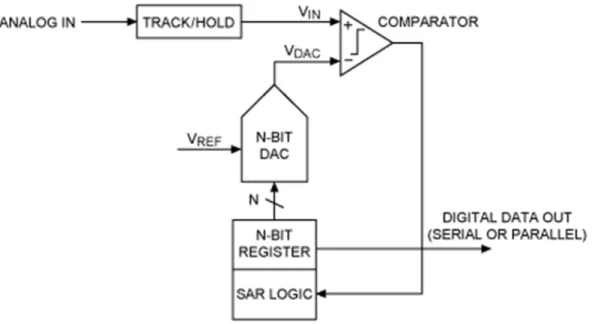
1.14 A simple Successive-Approximation-Register(SAR) ADC contains a comparator, SAR logic block, track/hold circuitry, and a DAC array. . . 28
1.15 The CC1111 features and contents. . . 28
2.1 A composite slab containing materials of di↵ering thermal conductivites. . . 30
2.2 Thermal model of the TEG and wristband heat-sink system. . . 31
2.3 The heat-sink thermal resistance is composed of the plate and the boundary resistance. 32 2.4 Simulation of thermal resistances of the various components of the heat-sink system as a function of BiTe element length. . . 33
2.5 The simplified thermal model of the heat-sink system, for power optimization. . . 34
2.6 A voltage source with an internal impedance and load to show power optimization. . 34
2.7 Thermal and electrical domains of the TEG and heat-sink system. . . 35
2.8 Output power density of the TEG given particular lengths of the BiTe elements [41]. 36 2.9 Patterned designs for maximizing the convection coefficient. . . 37
2.10 Finite-elements results for the di↵ering surface areas. . . 38
2.11 The temperature distribution of the plain heat-sink design. . . 38
2.12 The pitch of the length-grooved heat-sink. . . 39
2.13 The output voltage was reduced by increasing pitch due to a decrease in surface area. 39 2.14 The completing of the rolling process yields circularly shaped wristband, with imper-fect contact between the TEG and cold-side plate. . . 40
2.15 The press flattened the contact area surrounding the cold-side of the TEG. . . 40
2.16 Test set up to characterize the thermally insulating felt. . . 41
2.17 Characteristics of the thermal felt when placed on the arm, left, and on the hot plate, right. . . 41
2.19 The output voltage for the various heat sinks plus TEG systems as a function of time. 43 2.20 The optimum power output was measured by connecting a 10⌦ resistor as the output
electrical load. . . 44 2.21 The setup for the field test used a commercial DC/DC Converter as well as a voltage
logger. . . 45 2.22 The data collected from the 80-minute field test shows not only the TEG output (also
the DC/DC Converter input), but also the T of the TEG and the output of the DC/DC Converter. . . 46 2.23 A model and image of a body-powered LED system are shown. . . 46 2.24 The quantitative characteristics of the LED-loaded DC/DC Converter output are
shown, along with the DC/DC Converter output as well as the TEG voltage output and temperature di↵erential. . . 47 2.25 A model and image of the test setup used to characterize the wireless transmission
abilities of the TEG and checkerboard heat sink source. . . 48 2.26 The user-interface provided with the EnOcean kit records any incoming transmissions
from the EVA120+STM110 transmitter board. Screenshots of two di↵erent times after beginning communication with the board are shown. . . 48 2.27 A power sweep was conducted with the appropriate mean wireless transmission time
plotted for each input power level. . . 49 3.1 Unidirectional and bi-directional flex patters [46]. . . 52 3.2 Flex TEG design. . . 52 3.3 Top view of the flex kapton layer. Each island is interconnected with the flex patterns. 53 3.4 The inclusion of the flex strips yielded a lower temperature di↵erential when compared
with just replacing the strips with more copper. . . 54 3.5 Single flex TEG island finite-analysis results. . . 55 3.6 The uncut TEG required laser cutting of the slits within each TEG island as well as
cuts around the electrical traces. . . 56 3.7 The product of the laser cut yields kapton slits on each island for the placement of
the TEG arrays. . . 56 3.8 A thin copper sheet was cut into area equal to that of each individual TEG island.
Adhesive was used to append the copper and the cut kapton. . . 57 3.9 Two TEG arrays are shown after being cut with a 20µm dicing saw. . . 58 3.10 A side view and top view of the populated flex TEG is shown. . . 58 3.11 Upon thermally connecting the cold side copper strips with the ceramic, the flex TEG
is ready for curing of the TIM (the white sticker was used to hold a thermocouple for thermal measurements). . . 59 3.12 The flex TEG’s open-circuit voltage and temperature di↵erence were measured as a
function of time. . . 60 3.13 The performance of the flex TEG was recorded when worn around the upper forearm. 60 4.1 A block diagram highlighting the various sub-blocks of the EKG system is shown. . 65 4.2 The proposed EKG system contains not only the centralized processing circuitry but
also the EKG legs, which serve to acquire the EKG signal as well as generate the necessary energy from the body. . . 66 4.3 The top and bottom layers of the EKG legs are shown. The top layer consists of
the TEG voltage traces (VT EG+ and VT EG ), whereas the bottom consists of the
appropriate EKG probe pad input (VEKG). . . 67
4.4 The circuit diagram for the EKG processing and voltage regulation is shown. . . 68 4.5 The chip requires the EKG probes, supplies, and program lines as inputs. Apart from
the N-bit ADC output, the ROCLK is used to test if the chip was programmed properly. 70 4.6 The positive edge-triggered chip reads the SIN on the appropriate edge of SCK. SLD
indicates when the data is ready to be grabbed by the chip. . . 70 4.7 The Chipcon CC1111 board and debugger were used to program the front-end and
4.8 The SLD, SIN, and SCK signals generated from the microcontroller are shown. The sequence was repeated to ease capturing the waveforms on a network analyzer, thereby
containing an initial SLD pulse. . . 73
4.9 The schematic and corresponding PC Board design for the flex EKG’s processing circuitry is shown. . . 74
4.10 The footprint for the front end amplifier and ADC chip package is shown. The pin width and length were also specified. . . 75
4.11 The electrical connection between the EKG legs and the CPCA is made with solder paste as well as material epoxy. . . 75
4.12 The printed CPCA, shown, has a diameter of 6.4cm. . . 76
4.13 Due to the minimal thickness of the board, it may be bent and folded as shown. . . 77
4.14 The populated CPCA (minus the jumpers) is shown. The two large components are 220µF capacitors for the input of the voltage regulation stage. . . 78
4.15 The input power and output voltage waveforms are shown for the 600mV, 1.2V, and 1.8V sources. . . 79
4.16 The input sequences to the various pins of the chip are shown. This mode is used to test the chip’s external oscillator functionality. . . 79
4.17 The output DATAVALID is approximately a 20% duty-cycled waveform. The ROCLK signal is also shown. . . 80
4.18 A test of the internal oscillator reveals the expected 20% duty-cycled DATAVALID signal. . . 80
B.1 The two stage topology was used in designing the EKG amplifier. . . 97
B.2 The layout for the amplifier as well as the corresponding schematic and dimensions are shown. . . 98
B.3 The specs for three di↵erent cases are shown. . . 99
B.4 The block diagram-level design of the DC/DC Converter is shown. . . 100
B.5 The internals of the Boost and Buck Blocks are shown. . . 101
B.6 The output waveforms, divided into four phases, of the Boost Block and the Buck Block after a 50mV input was applied. . . 102
B.7 A block diagram-level SAR ADC is shown. . . 103
B.8 The comparator contains a pre-amplifier stage followed by a cross inverter latch, and a final SR Latch in order to e↵ectively store its state. . . 104
B.9 The logic for the SAR block contains the sequencer and the code register. . . 104
B.10 The negative input of the capacitor converges correctly to the positive input of the comparator at VDD/2. . . 105
B.11 An input ramp, when applied to the ADC, yielded the following output waveform. . 106
B.12 The output of the DC/DC Converter plus 8-bit ADC when an input EKG waveform is applied is shown. . . 106
List of Tables
1.1 Summary of TEG and heat sink system performance . . . 18
1.2 Summary of current research in ultra low power boost converters . . . 23
1.3 Summary of current research in front-end, analog EKG circuits. . . 25
1.4 A list of specifications for the extracted front-end schematic, designed in 600nm pro-cessing. . . 25
1.5 Summary of current research in front-end, analog EKG circuits. . . 26
2.1 Material properties used in calculating thermal resistances. . . 33
2.2 Material properties for BiTe. . . 36
3.1 Material properties of 1 mil copper and 1 mil kapton. . . 53
3.2 Internal Impedance and Power Characterization of the flex TEG. . . 61
Chapter 1
Introduction
1.1
Overview
The utilization of energy harvesting in running low power, bio-monitoring applications has become more prevalent with the advent of new circuit design techniques and technologies. Thermoelectric generators (TEGs) are of particular interest in body-worn energy harvesting due to their ability to generate power from a temperature gradient between the ambient and the skin [2]. Apart from the ability to harvest energy from arbitrarily small temperature di↵erences, the absence of moving parts is another appealing factor in utilizing such a device for energy harvesting. As with all heat engines a temperature di↵erential is required to generate power, in this case an e↵ective heat-sink is required to maintain a temperature di↵erential across the module. This thesis not only addresses main issues with existing types of heat-sinks in wearable applications, but also introduces a new type of thin, wearable, conformal, and comfortable heat-sink which aims to solve the issues of maintaining a temperature di↵erential across the body. Additionally, this 2-D heat-spreading technique is applied in not only the design of a flexible TEG, but also in an ultra-low power Electrocardiograph (EKG) acquisition and processing unit which, due to its power-hungry nature, provides a foundation for self-sufficiency. Ultimately, such a stand-alone, body-powered, EKG system may be used to continuously monitor patients within a care center or be deployed around the world and aid in monitoring the vitals of soldiers, all while avoiding the need for battery replacement.
1.2
Thermoelectric Generators
1.2.1
Seebeck E↵ect
Thermoelectric generator (TEG) behavior is characterized by the Seebeck E↵ect, which details the conversion of a temperature gradient across a conductor into a voltage [4, 6]. More specifically, when considering a single electrically conducting pipe, say, with a temperature gradient across its length, conduction charge carriers (either holes or electrons) will flow away from the hot side of the pipe towards the cold side. This net flow of charge yields an electric potential build-up called the Seebeck voltage. This voltage, V , is defined as follows:
V = S T, (1.1)
where S is the Seebeck coefficient and T is the temperature di↵erential across the conductor. In order to utilize this Seebeck voltage, one cannot simply connect probes across this conductor and expect a usable voltage. Due to the probe itself developing a Seebeck voltage, an inherent thermocouple is formed between this conducting pipe and the probe. If, however, the probe and the pipe were made of materials with di↵ering Seebeck coefficients, a net voltage may be expected from the system. In general, a thermocouple relies on di↵ering Seebeck coefficients to generate a voltage from a temperature gradient, as illustrated in Figure 1.1.
The Seebeck voltage across a thermocouple containing two di↵ering conductors then becomes
V = Z T2
T1
(SM etal1(T ) SM etal2(T ))dT (1.2)
where SM etal1(T ) and SM etal2(T ) are the respective, temperature-dependent Seebeck coefficients of
the two metals composing the thermocouple, and T1 and T2are the cold and hot side temperatures.
This principle may be applied to the TEG, where the two conductors of the thermocouple are doped n-type and p-type semiconductors. Notice that, now, when a temperature gradient is applied, holes (h+ in Figure 1.2) in the p-type and electrons (e-) in the n-type di↵use away from the hot source. This is apparent when examining the polarity of the Seebeck coefficient for n-type and p-type materials, where p-p-type have a positive coefficient and n-p-type a negative coefficient. And, since holes moving in the one directions is equivalent to electrons moving in the other, a closed circuit is formed between the thermocouple and the load. By arranging hundreds of thermocouples in this electrically-series, thermally-parallel pattern, the Seebeck voltage across individual thermocouples is added linearly, as shown in Equation 1.3.
V = N ↵couple T (1.3)
Here, V is the open-circuit voltage across the TEG, N is the number of p-n thermocouples, ↵couple
is the Seebeck coefficient, and T is the temperature di↵erential.
Figure 1.2: The internals of a TEG, focusing on a single thermocouple upon applying a temperature gradient [5].
1.2.2
Thermoelectric Composition and Materials
A typical TEG module, shown in Figure 1.2, contains two ceramic layers surrounding a patterned semiconductor layer. The ceramic top and bottom surfaces are required in part for structural stability
as well as for ceramic’s inherently low electrical conductivity and high thermal conductivity. These properties are important in not only providing electrical insulation within the semiconductor layer, but also to ensure maximum heat transfer from one side of the ceramic material to the other due to its high thermal conductivity.
Further inspection of the semiconductor layer, see Figure 1.2, reveals doped n-type and p-type semiconductor material. Each module contains numerous thermocouples, which contain a single n-type and p-type semiconductor connected with an electrical junction. The two-terminal thermo-couples are arranged in an electrically-series, thermally-parallel pattern, where one thermocouple’s n-type block is connected to another’s p-type block. More specifically, all p and n blocks see the same hot and cold side temperatures resulting in every thermocouple being in a thermal series con-figuration. However, the two terminals of the n block connect to di↵ering but adjacent, p blocks.
This pattern is repeated hundreds of times per module, resulting in a few hundred n-type and p-type blocks.
Modern TEGs are typically created using bismuth telluride (Bi2T e3) due to its economic
fea-sibility and relatively high efficiency at low temperatures [8]. High efficiency at low temperature gradients is critical for body-wearable applications, where the gradient is generally on the order of 2-4 degrees Celcius. Lead telluride (P bT e) and Uranium Dioxide (U O2) are other researched
alternatives [10, 11]. This work primarily utilizes Bi2T e3 modules.
1.3
Heat Sink Design
1.3.1
Background and Current, State-Of-the-Art Research
In order to maintain a working potential across a TEG, a heat sink is added to the system to ensure a finite heat flow through the module. Cold-side cooling may be accomplished in many ways. However, convection cooling utilizing the ambient air flow is the most common technique, especially for body-powered applications, where other means of cooling are difficult to incorporate.
Dimensional and material properties of the heat sink should be taken into careful consideration while designing a power-optimized TEG and heat sink system. This concept is further explored in Chapter 2. Current research in body-powered, TEG-based systems target low power applications with the intent of powering watches or other small applications. Figure 1.3 shows some examples of TEG-based wearable applications.
The head band in Figure 1.3 generates 2.5mW of power, translating into a power density of 20 µW/cm2. The watches in the same figure generate 150 to 200 µW of power at 0.8 to 1.2V
open-Figure 1.3: Current TEG-based wearable applications
circuit voltage. Such power values may be used in running many micro-power applications including those targeted towards human vital monitoring, such as heartbeat sensors and pulse oximeters [9].
1.3.2
Wearable, Low Profile, 2-D Heat-Spreader
One of the major drawbacks of utilizing the TEG-based applications in Figure 1.3, apart from their minimal power output performance, is the relative thickness of the system as well as the weight of the system. In particular, the thickness of the system is on the order of tens of millimeters, with the headband being about 30mm and weighing about 2 pounds. Such a thickness is essential for this design due to the utilization of the typical, 3-D heat-spreading technique, where cooling is attained through extending as far away from the hot source as reasonably possible, thereby increasing the surface contact area with the ambient coolant. The watches also follow this trend and extend 20mm away from the cold-side. This poses many problems in ensuring comfortableness of the system when worn. Apart from this issue, the relatively small contact surface of the heat sinks and the lack of conformity pose issues in maintaining proper contact between the hot source and the TEG, which in turn results in output power fluctuations.
Figure 1.4: The wearable, wristband heat sink ensures that the system remain comfortable and e↵ective. A model and image are shown [41].
The designed 2-D heat-spreading wristbands, shown in Figure 1.4, take these issues into account. Firstly, by limiting heat flow in only two dimensions (ie only along the contour of one’s arm), a low profile is maintained. Additionally, by utilizing the large available surface area of the arm, the heat sink successfully maintains a working temperature di↵erential comparable with that of current research. However, rather than extending more than 20mm away from the hot source, the 2-D wristbands have a thickness of under 5mm, which includes the thickness of the TEG. Additionally, a byproduct of utilizing a large surface area is the increased contact provided between the hot body and the hot-side of the TEG. Tests show that moving or rotating the arm yields minimal contact loss. The design choices and characterization of these heat sinks is further analyzed in Chapter 2. A comparison of the performance, variations, and dimensions of the systems in this work as well as in current research is summarized in Table 1.1. Notice that multiple cold-side groove patterns have been explored and tested. The groove patterns are illustrated in Figure 1.5 and their appropriate performances are listed in Table 1.1.
Figure 1.5: The flat(left), length-grooved(middle), and checker-board(right) heat sinks are illustrated.
1.3.3
Flexible, Stretchable TEG
The concept of 2-D heat-spreading extends beyond the wristband heat sink system introduced in Section 1.3.2. The design of a flexible TEG system, shown in Figure 1.6, allows for further leniency when approaching the concept of a universal energy harvesting system. More specifically, the di-mensions of the wristband heat sink limited its use to those with appropriate arm widths. However, by designing a flexible heat sink, a wider range of individuals may comfortably wear the harvester. In addition, by cutting each individual TEG module into arrays with a width of two elements and placing them on interconnected “islands”, a more uniform heat distribution across the cold-side heat sink is expected.
The design illustrated in Figure 1.6 parallels that of the wristband heat sink. However, the TEG module in the wristband is cut into arrays. These arrays, in turn, are coupled with a cold-side copper heat sink and a hot-side copper sheet for better contact in order to form islands. The hot-side copper sheet also contains electrical traces to series-connect the arrays. The various components of each
Name Open Circuit Voltage (mV) Load-matched, optimum power(µW) Power Density (µW/cm2) Heat sink system dimensions (L, W, H) Reference Miniaturized thermoelectric generator for human body applications 150 0.0003 ⇡0.00173 4.5cm x 2cm⇡4.5cm x [12] Flexible Thermoelectric Generator for Wearable Biometric Sensors 160 0.00418 ⇡ 0.00019 0.7cm x 0.3cm x 500nm (thin-film) [13] Wearable Head-Band – 2500 ⇡ 17 30cm x 5cm⇡ 3cm x [14] Seiko Thermic wristwatch 3000 30 ⇡ 26 5.5cm x 2cm⇡ 5.5cm x [15] Coin-size coiled-up polymer foil thermoelectric power generator 750 10 ⇡ 1.1 1cm x 1cm x 1cm [16] Checkerboard, wearable wristband heat sink 91 280 25.0 25.2cm x 6.4cm x 0.1cm This work Length, wearable
wristband heat sink 82 215 19.4
25.2cm x 6.4cm x
0.1cm
This work Flat, wearble
wristband heat sink 80 190 17.6
25.2cm x 6.4cm x 0.1cm This work Flex TEG 20 11 0.13 17cm x 5cm x 0.1cm This work
Table 1.1: Summary of TEG and heat sink system performance
island are thermally bonded using thermal paste. Each island is interconnected to adjacent islands through the utilization of flex traces [46]. These flex traces enable 1-D stretching along the length of the circuit. Notice from Figure 1.6 that the flex traces are bent in such a way as to allow the TEG islands to compress and expand. Initial tests of the designed flex TEG yielded stretching up to 30% of the original length. Each flex TEG contains three individual TEG modules, which were cut into arrays. This yielded matching thermal impedances between the modules and the heat sink. Current design shows a 20mV open-circuit voltage and approximately 40 µW of power. The design and performance of the flex TEG are further explored in Chapter 2.
Figure 1.6: A model of the flex TEG is shown.
1.4
Applications
1.4.1
Motivation and Goal
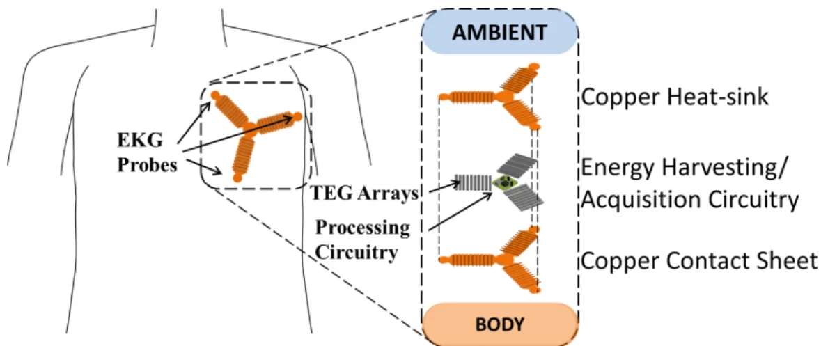
Figure 1.3 showed some example systems utilizing body-powered TEG systems as the main supply. Applications targeted towards medical monitoring are of particular interest due to their power hungry nature and packaging advantages. This work details the creation of a body-powered, EKG acquisition and processing unit. A model of the system is shown in Figure 1.7. The overall system rests on the user’s chest and contains not only 2-D heat-spreading TEG arrays for power, but also the EKG probes and processing circuitry.
Figure 1.7: A model of the body-powered EKG acquisition system containing the various layers is shown.
1.4.2
EKG System
Overview
A high-level diagram of the processing circuitry as well as the TEG supply and receiver is shown in Figure 1.8. The processing circuitry contains a boost converter, EKG front-end circuitry, an 8-bit analog-to-digital converter (ADC), an ultra-low power Digital Signal Processor (DSP), and a wireless transmitter. The objective is to acquire one’s EKG waveform from the front-end circuitry, digitize the signal using the ADC, perform simple processing in the DSP, and transmit the compressed data to a receiver connected to one’s computer. In doing so, power is supplied to these blocks using only the body-powered TEG arrays. These sub-blocks will be individually analyzed in more detail below.
Figure 1.8: A high-level block diagram representation of the EKG acquisition system is shown.
Introduction to EKG
An EKG (Electrocardiography) is a tool to measure the health of ones heart. The various states of polarizations of the heart during a cardiac cycle yield measurable electrical signals on one’s skin. The interaction between the four chambers of the heart results in a two-phase pumping action, known as diastole and systole. During the diastole phase, blood fills up the heart and during systole, this blood rushes to the bodys organs [9]. Each phase requires a unique set of actions to be performed by the four chambers of the heart. A byproduct of these actions is a noticeable potential di↵erence
between di↵ering parts of the body.
Figure 1.9: A sample EKG waveform with the two phases is highlighted.
A typical EKG waveform, shown in Figure 1.9, amplifies the di↵erence in voltage between elec-trodes placed on the skin. Conducting gel is used to ensure proper contact and a stronger signal. The electrode locations are based on the dipole-like nature of the heart. Experimentation led to further accuracy in probe placement [18]. By strategically placing these probes and amplifying the resulting electrical di↵erence, various stages of the EKG pulse may be observed. More specifically, every period of a pulse contains noticable P, Q, R, S, and T waves. These waves are generated due to some combination of the aortic and mitral valves opening or closing. By observing the duration and magnitude of these various waves, such medical issues as cardiac murmurs, seizures, arrhythmias, and cardiac dysrhythmias may be detected [24].
DC-DC Converter
The necessity of a DC-DC Converter becomes evident when handling sub-volt input supplies, which are prevalent in TEG-based applications. DC-DC Converters provide a means of using, say, a 100mV input voltage to drive analog and digital circuits by first boosting this input to an approximately usable 2.0V. By doing so, issues such as subthreshold leakage in digital circuits and inadequate linear range in analog circuits are avoided [31].
A simple, synchronous boost converter topology is shown in Figure 1.10, with the Supply provid-ing a low input voltage and the Load seeprovid-ing a higher output voltage. By varyprovid-ing the pulse width of the switch, current storage in the inductor and the following “discharge” into the capacitor produce
Figure 1.10: A basic boost, DC-DC Converter topology contains an inductor, switch, diode, and capacitor.
a dependent output voltage. More specifically, a boost converter’s transfer functions is as follows: Vout
Vin
= 1
1 D, (1.4)
where Vout and Vin represent the high output voltage and low input voltage, respectively, and D
is the duty cycle of the switch. With a duty cycle approaching one (switch is always closed), the inductor current continuously builds up and results in a Vout approaching 0V. As the switch opens,
the current in the inductor is dumped onto the capacitor. The presence of the diode ensures that no back-current flows upon charging the capacitor.
Although functional, imperfections in the form of finite resistance in the inductor and capacitor as well as a non-zero voltage drop across the diode result in such a design being infeasible for high efficiency, low power applications. Modifications and additions have been made to this base design in order to ensure proper operation with a higher efficiency. Techniques such as cascading a boost converter followed by a buck converter yield better control over the output [32]. Additionally, incorporating digital control of the switch in both stage yield higher efficiencies and lower leakage. Table 1.2 shows the current state-of-the-art boost converters and their efficiencies.
The modified boost converter topology used in this research, which incorporate the modifications detailed above, is shown in Figure 1.11. The circuit contains multiple blocks serving to either control the output, or generate reference and clock signals. In this case, the ST ART block utilizes a mechanical actuator (switch S1) and at least a 35mV input voltage, VT H, in order to begin
generating the reference voltages and clock signals. The ST ORAGE block takes the VT H input and
also a supply input, VDD, in order to boost the output voltage, VST O, up to a value higher than
Name Input Voltage (V) Output Voltage (V) Peak Efficiency (%) Reference Batteryless Thermoelectric Energy-Harvesting Interface Circuit 35mV 1.8V 58% [32] EnOcean ECT310 20mV-250mV 4V 30% [33] 20mV Input Boost Converter 20mV 1V 50% [34] LT Ultralow Voltage Step-Up 20mV - 1V 2.2V 60% This work, [35] 50mV Input Low Power Boost Converter 50mV 1.8V 60% This work
Table 1.2: Summary of current research in ultra low power boost converters
converter ensures more accurate control of the output voltage, since Vout
Vin = D, (1.5)
rather than being inversely proportional to the duty cycle in the case of the boost converter.
EKG Front-End Circuitry
Current research in acquiring an analog EKG signal is detailed in Table 1.5. A majority of the work, including this work, relies on a two-stage amplifier topology. However, some of the front end amplifier research in Table 1.5 include work done on larger subsystems as well.
The Ultra Low Power EKG from Table 1.5 for this work utilizes a three probe, EKG front-end topology, shown in Figure 1.12. The probes, labeled Zlef t, Zright, and Zgnd, are generally located on
the left hand, right hand, and leg, respectively. However, for packaging convenience, the probes may be placed as shown in Figure 1.7. This front-end topology aims to not only amplify the di↵erential voltage generated between the Zlef t and Zright probes, but also uses the Zgnd probe to feedback
and reject 60Hz common mode noise (shown in Figure 1.12 as v60Hz). Due to the inherent
high-impedance nature of the human body, 60Hz noise is especially prevalent. By using the Zgnd probe
as an active ground which feeds back into the body, a much cleaner di↵erential voltage is observed [25].
A circuit-level schematic of the topology in Figure 1.12 is shown in Figure 1.13. The Signal Amplifier block contains two gain stages, with the first stage (composed of amplifiers M1 and M2
Figure 1.11: A 35mV input boost converter [32] is shown. Further discussion will continue in Chapter 4.
in Figure 1.13) performing di↵erential amplification of the Vin+and Vin probe inputs. The second
gain stage, composed of amplifier M3, further gains this di↵erential signal. The output of the first
stage passes through amplifier M4, capacitor C11, and a super bu↵er before being fedback through
the body. This feedback path contains an integrator in the form of the C11 capacitor. The various
amplifiers are designed as simple transconductance amplifiers with pmos current mirrors and nmos biasing transistors. Specifications for the front-end layout are shown in Table 1.4. The specifications were rendered in Cadence, using 600nm AMI CMOS processing. The layout characteristics are further explored in Chapter 4.
Analog-to-Digital Converter (ADC)
The interface between the DSP and the analog real world occurs through the ADC. By converting an analog waveform such as an EKG output into, say, an 8-bit digital bus, further processing of the data may occur using a microcontroller or Field-Programmable-Gate-Array (FPGA).
The Successive-Approximation-Register (SAR) ADC is generally the ideal choice for low power, high efficiency, and medium to high resolution applications and will be utilized in this work[36]. Table 1.5 shows the performance of current SAR ADC. Appendix B of this work looks further into the design and testing of a SAR ADC in 90nm processing.
Name Processing Technology Operating Voltage (V) Power (µW) Reference Analog CMOS Processing Chip for ECG 0.35µ 3.3V 72.6µW [26] Sub-threshold Mixed-Signal ECG SoC 0.13µ 0.8V 2.6µW [27]
Flexible SoC for Biomedical Signal Acquisition
0.35µ 3.3V 66µW [28]
Micropower EKG 0.5µ 1.5V, 3V 2.1µW [29]
Sensor Interface for Biomedical Applications 0.18µ 600mV, 1.2V, 1.8V 2.5 µW This Work, [30]
Ultra Low Power EKG 0.6µ 2.1V 10µW This Work
Table 1.3: Summary of current research in front-end, analog EKG circuits.
Table 1.4: A list of specifications for the extracted front-end schematic, designed in 600nm processing. Common mode rejection -60.89 dB Di↵erential Gain 42.96 dB CMRR 103.825 dB Noise 6.133 µV Bandwidth 2.2 kHz Power 4.587 µW DSP and Transmitter
The DSP and Wireless transmitter used in this work are a part of the Chipcon family. The CC1111 is a system-on-chip (SoC) with a built-in microcontroller unit, memory, an RF Transmitter, and a USB controller. The microcontroller contains an 8051 core and various sleep modes. In addition, a supply passes through a voltage regulator before entering the SoC. Complete peripherals of the CC1111 are shown in Figure 1.15.
1.5
Power Management and Efficiency
The measured power budget from the wristband heat sink is approximately 300 µW at steady state. A major source of system optimization comes in the form of trade-o↵s between on chip processing plus compression and packet size transmission. More specifically, the issue of finding a balance between continuous data transmission with minimal on-chip processing and maximum on-chip processing with
Figure 1.12: A sample EKG front-end topology is shown [19]. Name Analog Input Range (V) Digital Output Resolution Power Consump-tion Reference SAR ADC for
Distributed Sensor Networks
0 - 1V 8-bit 31
pJ/sample [20]
12-bit Rate-resolution
SAR ADC 0 - 1V 12-bit
200nW at
500 S/sec [21]
Low Power SAR ADC for Bio-medical Applications
0 - 1V 8-bit 7.75 µW at
500 kS/sec [22]
0.5V, 1 µW SAR ADC 0 - 1V 8-bit 0.85 µW at
4.1 kS/sec [23]
8-bit Ultra-low Power
SAR ADC 0 - 1.8V 8-bit
2 pJ/sample
at 1.25 MHz This work Table 1.5: Summary of current research in front-end, analog EKG circuits.
minimal packet size transmission will be further explored in Chapter 4.
1.6
Thesis Organization and Contributions
The need for conformal, low-profile TEG-based heat sink systems is essential for maintaining com-fortableness in not only energy harvesting but also in medical monitoring. By applying the concept of 2-D heat-spreading to create flexible TEGs and flexible EKG processing modules, patients and soldiers are better suited to using such self-sustaining applications. This thesis hopes to produce a viable alternative for heat sink design as well as body-powered applications of any sort. Chapter 2 begins by delving into the theory behind heat sink optimization through thermal impedance
match-Figure 1.13: A detailed schematic of the three-probe EKG front-end circuit [19].
ing. This concept will be applied in determining the dimensional and material characteristics of the heat sink for the TEG. Additionally, the same concept will be applied in the design of the flexible TEG. Moving on, Chapter 3 will characterize not only the wristband heat sinks from Figure 1.5, but also the flexible TEGs. Both simulation data as well as experimental results will be shown. Chapter 4 applies the 2-D heat-spreading technique to the design of a flexible EKG patch, placed around the heart. Lastly, Chapter 5 concludes and provides possible future paths for this thesis.
Figure 1.14: A simple Successive-Approximation-Register(SAR) ADC contains a comparator, SAR logic block, track/hold circuitry, and a DAC array.
Chapter 2
Thermal Impedance Optimization
and the Wristband Heat Sink
System
2.1
Motivation and Organization
Current wearable, TEG-based systems, due to their minimal contact with the skin and large thick-ness, maintain a high profile when worn, which translates to a lack of comfortableness. Additionally, the minimal surface contact area poses issues when the body is in motion, yielding di↵ering hot-side contact. This chapter introduces the theoretical models and experimental results obtained for the 2-D wristband heat sink. The chapter begins with an overview to the concept of thermal circuits, which is essential for setting up the theoretical models. Next, in Section 2.3, the thermal model of the 2-D heat sinks are introduced, taking into consideration the various approximations made to simplify the analysis. Additionally, the concept of heat sink optimization shall be applied in order to ensure a maximum power output in a “heat sink-limited regime”. In Section 2.4, experimental setups and results for the various heat sinks will be detailed, with design limitations in mind and exploration into powering various load applications. Lastly, Section 2.5 will conclude by providing possible avenues for improvement and set a foundation to Chapter 3.
2.2
Introduction to Thermal Circuits
The integral form of Fourier’s Law of thermal conduction yields a relationship between the heat flux through a body and the temperature di↵erence across the body such that
Q
t = kA
T
x (2.1)
where Qt is the heat flux, T is the temperature di↵erence, k is the thermal conductivity, A is the cross sectional area, and x is the length of the object. Ohm’s Law is the electrical analogy to this expression and states that
i = V
R (2.2)
where i is charge per time or current, R is the resistance, and V is the voltage di↵erence across the element. By studying Equations 2.1 and 2.2, it becomes apparent that the equivalent electrical analogy to thermal heat flux is current and the equivalent analogy to temperature di↵erence is voltage. Notice also that the thermal resistance of a material is defined as
Rthermal=
x
kA. (2.3)
These principles may be applied to characterize thermal environments where multiple materials of di↵ering characteristics are involved. For example, Figure 2.1 shows two separate materials within a composite slab where the heat flux, Qt or equivalently ˙Q, is conserved but a temperature di↵erence exists between each material[38].
Figure 2.1: A composite slab containing materials of di↵ering thermal conductivites.
The equivalent resistances, R1 and R2 are
R1=
x1
k1A
R2=
x2
k2A
(2.5) and, with series resistances in mind, the relationship between the heat flux and temperature di↵erence is
˙
Q = T2 T1 R1+ R2
(2.6) This example shows that a clear parallel exists between the electrical and thermal domains and the behavior of temperature gradients and heat fluxes is analogous to voltage and current.
2.3
Theoretical Analysis of 2-D Wristband Heat-Sink
2.3.1
Thermal Model
Similar to the composite slab, the TEG and wristband heat-sink system may be modeled as a series of resistances connected between two temperature sources, in this case that of the ambient and the skin. Figure 2.2 shows not only a cross-section of the various materials composing the system, but also the equivalent thermal circuit.
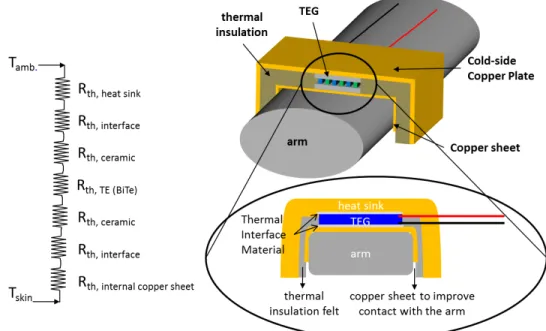
Figure 2.2: Thermal model of the TEG and wristband heat-sink system.
The wristband heat-sink system contains not only the top copper plate utilized for cold-side dissipation but also a thin copper sheet in contact between the hot-side of the TEG and the skin. The purpose of the cold-side copper sheet was experimentally determined to provide a better contact
between the rigid TEG module and the skin, and will be explored further in Chapter 3. The system also contains thermal interface material (TIM) in order to thermally adhere the copper with the hot and cold sides of the TEG. Lastly, the TEG itself is comprised of two ceramic plates sandwiching the Bi2T e3 elements. Each of these various layers is modeled by individual resistances beginning with
Rth,heatsink for the cold-side copper plate, then Rth,interf acefor the TIM, Rth,ceramicfor the hot-side
TEG ceramic, Rth,T E(BiT e) for the TEG elements, Rth,ceramic and Rth,interf ace for the cold-side,
and finally Rth,internal copper sheet for the hot-side copper sheet.
Imperfect contact between any material boundary may be modeled with an appropriate interface conductance (or convection coefficient), h [39]. The relationship between the convection coefficient and thermal resistance is
Rth,contact= 1
Ah, (2.7)
where Rth,contact is the thermal resistance of the contact surface, A is the cross sectional area (ie
orthogonal to the heat flux), and h is the convection coefficient. In this case, a boundary exists between the cold-side heat-sink and the ambient environment. Revisiting the thermal circuit in Figure 2.2, the resistance of the heat-sink, Rth,heatsink, may be subdivided, as shown in Figure 2.3
into not only the thermal resistance of the copper plate, Rth,platebut also the resistance attributed
to the convection coefficient, Rth,cc.
Figure 2.3: The heat-sink thermal resistance is composed of the plate and the boundary resistance.
Due to the relatively high thermal conductivity of copper, the heat-sink resistance is primarily composed of the interface component only. Thus,
Rth,heatsink= Rth,cc (2.8)
Additionally, the thermal model in Figure 2.2 may be further simplified to contain only the Rth,heatsink
con-ductivities of the copper sheet, ceramic plates, and TIM (ceramic-filled silicone) which, in turn, yield very low thermal resistances for these various components.
Material Thermal Conductivity (W/mK) Specific Heat Capacity (J/kgK) Density (kg/cm3) Copper 350 385 8920 TIM 2.3 1714 2530 Ceramic 35 880 3698 Bi2T e3 1.6 154.4 7740
Table 2.1: Material properties used in calculating thermal resistances.
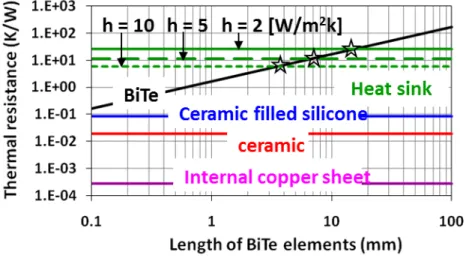
The various thermal resistances are quantified in Figure 2.4. The resistances are plotted with respect to the length of the Bi2T e3 elements. This is done to allude to the heat-sink optimization
issue which will be discussed in the next section.
Figure 2.4: Simulation of thermal resistances of the various components of the heat-sink system as a function of BiTe element length.
Notice, in Figure 2.4, the linear relationship between the thermal resistance and the length of the Bi2T e3 elements. In addition, the heat-sink impedance varies inversely with the convection
coefficient, h. Lastly, the relative resistances of the ceramic filled silicone (TIM), the copper sheet, and the ceramic places are more than two orders of magnitude below that of the heat-sink or TEG. As a result, they are ignored for simulation purposes.
To conclude, the original thermal model of the system from Figure 2.2 may be simplified to two resistances, as illustrated in Figure 2.5. The heat-sink resistance, dictated by the copper-air boundary, is a function of the convection coefficient, h, and the TEG impedance is dictated by the
length of the elements, LBiT e.
Figure 2.5: The simplified thermal model of the heat-sink system, for power optimization.
2.3.2
Power Optimization of the TEG and Heat-Sink System
Given a constant supply, V , an internal source impedance, Rint, and a load impedance, Rload, as
shown in Figure 2.6, the maximum power delivered to Rload occurs when
Rload = Rint (2.9)
Figure 2.6: A voltage source with an internal impedance and load to show power optimization.
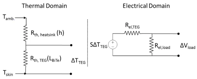
Similarly, from Figure 2.5, the heat-sink impedance may be viewed as an internal impedance and the impedance of the TEG may be the load. For optimum power from the TEG and assuming with a fixed heat-sink impedance, these impedances must match [40].
Thus far, optimization has occurred only within the thermal domain. However, operation of the TEG system in the electrical domain must be introduced before proceeding further. Figure 2.7 shows the system in entirety.
Figure 2.7: Thermal and electrical domains of the TEG and heat-sink system.
The conversion between the thermal and electrical domains is shown with a simple voltage supply, S TT EG, where S is the Seebeck coefficient of the module. Due to the changing nature of Rel,T EG,
which is directly proportional to the module length, and of Rth,T EG, which is inversely proportional
to the module length, power optimization must occur within the electrical and thermal domains combined. More specifically, utilizing very long BiTe elements yields a large TT EG. However,
Rel,T EG will be significantly large, thereby providing a low output power to the load. On the other
hand, making the elements short provides a small Rel,T EG. However, TT EGbecomes small, yielding
a small supply voltage. Approaching this more analytically, a “voltage-divider” exists between the ambient to skin temperature di↵erential and the temperature drop across the TEG. If we assume
T = Tskin Tamb. (2.10) Then, TT EG = Rth,T EG Rth,heatsink+ Rth,T EG T (2.11) Vload = S TT EG Rel,load Rel,T EG+ Rel,load (2.12) = Rel,load Rel,T EG+ Rel,load Rth,T EG Rth,heatsink+ Rth,T EG S T (2.13)
The power delivered across the electrical load, Rel,load, is thus,
Pel,load = V2 load Rel,load (2.14) = 1 Rel,load ( Rel,load Rel,T EG+ Rel,load Rth,T EG Rth,heatsink+ Rth,T EG S T )2 (2.15)
= Rel,load (Rel,T EG+ Rel,load)2 R2 th,T EG (Rth,heatsink+ Rth,T EG)2 (S T )2 (2.16)
From the material characteristic values from Table 2.1 and 2.2, a sweep of the power density may be performed given a particular TEG length.
Material Thermal Conductivity (W/mK) Seebeck Coefficient (µV /K) Electrical Conductiv-ity (1/⌦/m) BiTe [42] 1.47 240 73700
Table 2.2: Material properties for BiTe.
The results of the simulation for multiple convection coefficients are shown in Figure 2.8.
Figure 2.8: Output power density of the TEG given particular lengths of the BiTe elements [41].
The maximum power density, indicated with a star in Figure 2.8, is achieved when the thermal resistance of the heat-sink equals that of the TEG. This is equivalent to saying that the same temperature di↵erential exists between the heat-sink and the TEG [43, 44]. Notice also that this optimization step, that is, matching the resistances of the TEG and heat-sink, occurs in a heat-sink limited regime. More specifically, only upon optimizing the heat-sink design to provide the highest convection coefficient, h, should thermal resistance matching occur. This is explored further in the next section.
2.3.3
Convection Coefficient Maximization and Simulation Results
The convection coefficient, or heat transfer coefficient, as introduced earlier, is used to model heat transfer between materials of di↵ering phases [45]. It is characterized as follows
h = Q
A T, (2.17)
where Q is the heat flow, A is the surface area, and T is the temperature di↵erence. Since the power output from the TEG, from Equation 2.16, is inversely proportional to Rth,heatsink2, minimizing the
heat-sink impedance should be the first priority. Since the heat-sink resistance density is inversely proportional to the convection coefficient, from Equation 2.7, it is desirable to make h as large as possible. The only controllable means of doing so is to increase the surface contact area, A.
Three di↵erent designs with varying surface areas were explored, both through simulations as well as through experimentation. We focus now on the simulation results and explore the experimental results in Chapter 3. The three patterned designs for the cold-side heat-sink are shown in Figure 2.9. The thickness was maintained at 1mm for all designs. This ensured that the system was low-profile
Figure 2.9: Patterned designs for maximizing the convection coefficient.
and comfortable when worn. Additionally, the surface area in contact with the arm was held constant with dimensions of 29 cm x 6 cm. However, the cold-side surface area was modified through the utilization of unidirectional length grooves as well as bidirectional checkerboard grooves.
With grateful assistance from Dr. Katey Lo, finite-element analysis was performed on the three designs in order to accurately characterize the temperature distribution on the cold-side. The design assumed a temperature di↵erential of 10 C, with the skin temperature at 33 C and the ambient temperature at 23 C. Natural air convection, with h = 5W/m2K, was applied to the cold-side
copper heat-sinks. The results are shown in Figure 2.10.
The checkerboard wristband, with an increased surface area, did yield a lower thermal resistance as seen with the lower temperature di↵erential. Studying just the plain wristband system, it can be seen from Figure 2.11 that less than half the temperature between the ambient and the skin drops
Figure 2.10: Finite-elements results for the di↵ering surface areas.
across the TEG, yielding the conclusion that a better heat-sink with an increased surface area and better convection coefficient was necessary. Figure 2.11 takes advantage of the symmetric nature of the TEG and heat-sink system by simulating only one quarter of it. Similar temperature behavior is expected throughout the entire system.
Figure 2.11: The temperature distribution of the plain heat-sink design.
Initially, the temperature gradient across the TEG will be maximal due to the smaller e↵ective heat-sink impedance. However, at steady-state (which, experimentally, was approximately 7-10 min-utes after wearing the heat-sink), the performance was greatly hindered due to the poor convection coefficient of the heat-sink.
Exploring the geometry of the various groove patterns, analyses have been performed relating the open-circuit output voltage to the pitch of the grooves. The pitch, illustrated in Figure 2.12, is the length of the protruding copper in between the machined grooves.
Figure 2.12: The pitch of the length-grooved heat-sink.
By increasing the pitch, the relative surface area in contact with the ambient is decreased. As a result, a lower output voltage is expected. Indeed, this is what is observed and shown in Figure 2.13.
Figure 2.13: The output voltage was reduced by increasing pitch due to a decrease in surface area.
2.4
Experimental Procedure and Analysis
2.4.1
Fabrication
The prototypes in Figure 2.9 were fabricated utilizing copper with 1 mm thickness. The length and width were standardized for all designs to be 29.2 cm x 6.4 cm. Upon cutting the copper plates to this dimension, patterned grooves were made to one side. In order to generate the various groove patterns, a milling machine was used. The end-mill bit dimension, which controls the diameter of the grooves, was held constant at 0.5 mm for all variations of patterns. The pitches were varied from 5 mm to 9 mm. However, structural limitations of the copper led to a practical limit of pitch to 5 mm only. Surpassing this limit frequently led to the patterned copper plate snapping o↵ into multiple pieces when being shaped. The shaping of the flat copper plate into a circular wristband was done
with a roller. The plates were fed into the roller multiple times, with each pass curving the plate more and more. The rolling was complete after the left and right ends of the plate were roughly 3 cm apart. However, the circular shape of the cold-side copper plate posed issues with regards to contact with the TEG, as shown in Figure 2.14.
Figure 2.14: The completing of the rolling process yields circularly shaped wristband, with imperfect contact between the TEG and cold-side plate.
The large spacing between the ceramic and copper would require extensive use of the thermal interface material. This posed issues by adding to the thermal parasitic resistances and yielding a lower power output from the TEG. Rather, before the TEG was mounted to the heat sink, a press was used to flatten the area surrounding the contact region, as shown in Figure 2.15.
Figure 2.15: The press flattened the contact area surrounding the cold-side of the TEG.
A small aluminum block with dimensions slightly larger than that of the TEG was used as the foot-print for the press. The result was a much flatter surface which required less thermal interface material to thermally connect the TEG and copper.
Upon cutting, grooving, shaping, rolling, and pressing the copper plate, thermally insulating felt was appended to the underside of the plate using a strong bonding adhesive. The flat area of the
heat sink where the TEG rests, was left exposed with no insulating material.
Recall from Figure 2.2 that the thermally insulating felt was required to constrain heat flow through the TEG. Tests were performed to characterize the material and ensure an adequate thermal impedance. Figure 2.16 shows the set up to characterize the felt.
Figure 2.16: Test set up to characterize the thermally insulating felt.
The felt is placed in between two copper blocks, where one block is in contact with a hot source (hot plate). Thermocouple temperature sensors are placed in small holes drilled in the blocks. Thermally conducting paste is applied to provide the best thermal contact possible. The sensors are placed inside the blocks to ensure as accurate a temperature measurement for the hot and cold sides as possible. The results of this test, as well as a test replacing the hot source with a human arm itself, are shown in Figure 2.17.
Figure 2.17: Characteristics of the thermal felt when placed on the arm, left, and on the hot plate, right.
the other replacing the TEG with more felt. Not only does this show that the heat flux is indeed constrained to pass through the TEG with the felt providing thermal isolation, but also that 2-D heat spreading is being utilized as seen with the even temperature distribution on the cold side copper of the felt plus TEG-based heat sink. The insulating properties of the felt are further characterized in the hot and cold side temperature plot in Figure 2.17. Here, with a hot side temperature of 125 C in the bottom copper block, a cold side temperature of 48 C is maintained in the top block. The test was performed over the course of 85 minutes, giving adequate time to attain steady state behavior. Upon adhesively bonding the thermal felt to the cold side copper plate, a thin layer of TIM (thermal interface material) was used to thermally connect the TEG with the copper. A second layer of TIM was applied to the hot side ceramic, which in turn was connected to a thin copper sheet. This hot side copper sheet spread along the underside of the felt and TEG and ensured a higher thermal contact between the skin and hot side, even when the arm was in motion.
Figure 2.18: The completed checkerboard heat sink is shown.
A fabricated design for the checkerboard heat sink is shown in Figure 2.18. The cold side copper plate was painted black in order to more accurately characterize the temperature distribution using an IR camera. Copper’s high reflective index would have yielded an incorrect temperature measurement. By painting the heat sink black, the e↵ective index decreases and results in the IR image from Figure 2.17.
2.4.2
Tests and Results
Open-Circuit Voltage and Optimum Power Characterization
Tests were performed comparing the plain, length grooved, and checkerboard heat sinks. These tests were performed in controlled ambient temperature settings with minimal air flow for natural convection. In all cases, the heat sinks were placed on the upper forearm, similar to that shown in Figure 2.18. All voltage measurements to characterize the output of the TEG were done with a voltage data logger, capable of 1 mV resolution. Additionally, the hot and cold side temperatures were measured with temperature sensors, similar to that used in Figure 2.16, with 0.5 C resolution. The first series of tests performed were transient experiments, measuring the output voltage of the various heat sinks plus TEG systems. The results are shown in Figure 2.19.
Figure 2.19: The output voltage for the various heat sinks plus TEG systems as a function of time.
The trend of results in Figure 2.19 match that of the simulations introduced in Section 2.3. In par-ticular, due to the larger surface area in contact with the cold side ambient of the checkerboard heat sink, a higher open-circuit voltage is expected. The length grooved was predicted to do slight worse than the checkerboard but better than the plain. This prediction is matched in the experimental results in Figure 2.19 as well.
The optimum power output from the TEG given an electrical load match is shown in Figure 2.20. Notice that other designs, besides the checkerboard, length, and plain were tested. More specifically, the 12-dense checkerboard design was included, which doubles the length and width spacing between adjacent grooves. Additionally, grooves along the width of the heat sink were also made. The output behavior of the width and length heat sinks are expected to be the same due to the constant spacing of the grooves yielding the same e↵ective cold-side surface area.
Figure 2.20: The optimum power output was measured by connecting a 10⌦ resistor as the output electrical load.
For the power experiments, the load impedance was fixed at 10⌦. Thus, with this fixed load, the voltage across the load was measured with the data logger, and the power was calculated based on the following.
P = V
2
R (2.18)
Notice, again, that the performance trend matched the predicted model introduced in the previous section, with the checkerboard heat sink providing the maximum power density of 25µW/cm2 at
3.5 C, the length grooved following at 19.4µW/cm2 with 3 C, and the plain at 17.6µW/cm2 with 2.5 C. In all cases, the tests were run for approximately 8 minutes.
Field Test
The checkerboard heat sink system was used as the power supply for various load applications, such as DC/DC converters, wireless transmitters, and laser diodes.
To begin, more characterization of the checkerboard heat sink system was done beyond that shown above. More specifically, a field test was performed, where the TEG output was connected to a 20mV input threshold DC/DC Converter, which was a part of the EnOcean Thermal Energy Harvesting Kit, as shown in Figure 2.21 [33].
Figure 2.21: The setup for the field test used a commercial DC/DC Converter as well as a voltage logger.
The DC/DC converter is a completely stand-alone unit, requiring no external transformers or capacitors. The start-up voltage for the device is 20mV and the boosted output, open-circuit volt-age is approximately 4.15V. The maximum efficiency of the device is approximately 35%. Figure 2.22 shows an 80-minute field test, where the output of the checkerboard heat sink plus TEG was connected to the input of the DC/DC Converter. The hot and cold side temperatures of the heat sink were recorded as well as the input and output voltages of the DC/DC Converter.
Figure 2.22 also shows the states of the ambient environment during the 80 minutes (ie “Walking Outdoors”, “Walking Indoors”, etc.). During the “Walking Outdoors” phase, a relatively high air convection is observed, thereby yielding a higher average output voltage from the TEG. On the other hand, during the “Sitting Indoors” phase, not only was the e↵ect of air convection minimal, but the cold-side ambient temperature was hotter. This yielded a slightly lower output voltage. Yet, even with these fluctuations in the input, the DC/DC Converter’s output was relatively constant at 4.15V. Although a higher ripple was observed during the “Walking” phases, the overall average was maintained above 4V at all times.
Output Loads and Applications
The output of the DC/DC Converter and TEG, as it was providing a consistent voltage above 4V, was connected to various loads including LEDs as well as the EnOcean wireless transmitter and receiver system.
Figure 2.22: The data collected from the 80-minute field test shows not only the TEG output (also the DC/DC Converter input), but also the T of the TEG and the output of the DC/DC Converter.
LED Load To begin, a simple LED load was connected, as shown in Figure 2.23 and its optical characteristics were studied. From Figure 2.23, the LED is visibly illuminated at steady-state (or 10 minutes after the heat sink was worn). In this case, the checkerboard heat sink was used as the power supply.
Figure 2.23: A model and image of a body-powered LED system are shown.
Figure 2.24 shows quantified results of the test. The power output from the LED was measured using an optical power meter interfaced with MATLAB in order to record the transient data. The
![Figure 1.2: The internals of a TEG, focusing on a single thermocouple upon applying a temperature gradient [5].](https://thumb-eu.123doks.com/thumbv2/123doknet/14178972.475870/14.918.324.588.533.879/figure-internals-focusing-single-thermocouple-applying-temperature-gradient.webp)

![Figure 1.11: A 35mV input boost converter [32] is shown. Further discussion will continue in Chapter 4.](https://thumb-eu.123doks.com/thumbv2/123doknet/14178972.475870/24.918.189.755.127.410/figure-input-boost-converter-shown-discussion-continue-chapter.webp)
![Figure 1.12: A sample EKG front-end topology is shown [19]. Name AnalogInput Range (V) Digital Output Resolution Power Consump-tion Reference SAR ADC for](https://thumb-eu.123doks.com/thumbv2/123doknet/14178972.475870/26.918.194.707.131.387/figure-topology-analoginput-digital-output-resolution-consump-reference.webp)
![Figure 1.13: A detailed schematic of the three-probe EKG front-end circuit [19].](https://thumb-eu.123doks.com/thumbv2/123doknet/14178972.475870/27.918.249.673.110.459/figure-detailed-schematic-probe-ekg-end-circuit.webp)