Publisher’s version / Version de l'éditeur:
The Journal of Physical Chemistry Letters, 8, 14, pp. 3179-3184, 2017-06-21
READ THESE TERMS AND CONDITIONS CAREFULLY BEFORE USING THIS WEBSITE.
https://nrc-publications.canada.ca/eng/copyright
Vous avez des questions? Nous pouvons vous aider. Pour communiquer directement avec un auteur, consultez la
première page de la revue dans laquelle son article a été publié afin de trouver ses coordonnées. Si vous n’arrivez pas à les repérer, communiquez avec nous à [email protected].
Questions? Contact the NRC Publications Archive team at
[email protected]. If you wish to email the authors directly, please see the first page of the publication for their contact information.
NRC Publications Archive
Archives des publications du CNRC
This publication could be one of several versions: author’s original, accepted manuscript or the publisher’s version. / La version de cette publication peut être l’une des suivantes : la version prépublication de l’auteur, la version acceptée du manuscrit ou la version de l’éditeur.
For the publisher’s version, please access the DOI link below./ Pour consulter la version de l’éditeur, utilisez le lien DOI ci-dessous.
https://doi.org/10.1021/acs.jpclett.7b01503
Access and use of this website and the material on it are subject to the Terms and Conditions set forth at
Ultrafast carrier trapping in thick-shell colloidal quantum dots
Jain, Ankit; Voznyy, Oleksandr; Korkusinski, Marek; Hawrylak, Pawel;
Sargent, Edward H.
https://publications-cnrc.canada.ca/fra/droits
L’accès à ce site Web et l’utilisation de son contenu sont assujettis aux conditions présentées dans le site LISEZ CES CONDITIONS ATTENTIVEMENT AVANT D’UTILISER CE SITE WEB.
NRC Publications Record / Notice d'Archives des publications de CNRC:
https://nrc-publications.canada.ca/eng/view/object/?id=ccf3b48d-d77c-4a0b-880d-9ba271f59f3b https://publications-cnrc.canada.ca/fra/voir/objet/?id=ccf3b48d-d77c-4a0b-880d-9ba271f59f3bUltrafast Carrier Trapping in Thick-Shell Colloidal Quantum Dots
Ankit Jain,
§,∥Oleksandr Voznyy,
§,∥Marek Korkusinski,
†Pawel Hawrylak,
‡and Edward H. Sargent
*
,§§
Department of Electrical and Computer Engineering, University of Toronto, 10 King’s College Road, Toronto, Ontario M5S 3G4, Canada
†
National Research Council of Canada, Ottawa, Ontario K1A 0R6, Canada
‡
Department of Physics, University of Ottawa, Ottawa, Ontario K1N 6N5, Canada
*
S Supporting InformationABSTRACT: It has previously been found that Auger processes can lead to femtosecond carrier trapping in quantum dots, limiting their performance in optoelectronic applications that rely on radiative recombination. Using atomistic simulations, we investigate whether a shell can protect carriers from Auger-assisted trapping. For these studies we investigate CdSe/CdS core−shell quantum dots having total diameters reaching up to 10 nm. We find trapping lifetimes as fast as 1 ps for 2 nm shells, and we report that shells as thick as 6 nm are required to suppress trapping fully. The most efficient recombination mechanism is found to proceed through shallow empty traps, suggesting it can be suppressed by filling the traps through doping or external electrochemical potential. Our findings suggest that to achieve efficient light emission, surface traps have to be completely eliminated, even in thick-shell quantum dots.
T
he optoelectronic properties of colloidal quantum dots (CQDs) are strongly affected by surface passivation. Normally such surface passivation aims at elimination of defects that would otherwise lead to electronic trap states. The defects can be formed due to lattice mismatch at the interface in core− shell CQDs,1,2 incomplete passivation by ligands of the CQD surface,3,4 oxidation, and photodegradation.5−7 The resulting trap states cause nonradiative losses through trapping of the electron or hole, followed by recombination of this trapped carrier with a free or another trapped carrier, adversely affecting the performance of CQDs in light-emitting devices,8−10 quantum dot lasers,11 and biological tracking inside living cells.12−15Unfortunately, the identity of the mechanisms that dominate nonradiative losses in CQDs remains to be determined conclusively.16−18 The origins and roles of traps and non-radiative losses in CQDs have been the subject of extensive modeling and experiment.17−20 A wide range of explanations for the loss of radiative efficiency have been proposed, but a consensus has yet to emerge on the physical origins of the most abundant trap states and on the relative roles of phonons, electron transfer, and Auger effects in recombination.16−18 In addition, for each of these mechanisms, multiple trapping and nonradiative recombination pathways have been offered.17
To investigate these trapping mechanisms in depth, Califano et al.17,21−23 used pseudopotential-based atomistic modeling and demonstrated high trapping rates via an Auger-assisted process. While the authors found subpicosecond lifetimes, their studies were limited to filled traps only with quantum dot sizes below 4 nm and did not explore the role of shell thickness.
Here we use a fully atomistic tight-binding model, together with a perturbative treatment of electron−electron interactions, to study systematically how shallow and deep interface and surface traps determine the trapping rates of carriers in core− shell CQDs. We focus, in particular, on realistically sized wurtzite CdSe/CdS core−shell CQDs with up to 10 nm total diameter. We study trapping pathways through both empty and filled traps and the dependence of their rates on trap energy, trap delocalization, and shell thickness. We find subnanosecond time scales for a pathway involving two trapped holes and that it can be suppressed through the filling of traps with electrons. Another pathway involving hole trapping can be slowed to tens of nanoseconds with the aid of a 3 nm shell.
In real CQDs, traps can form at different spatial locations on the surface, and the exact nature of traps remains experimentally unknown. Therefore, we studied multiple trapping processes, and for each process we explored parametrically the effect of trap localization and trap depth. This exhaustive study leads to a conclusion that no matter what the trap energy is there will always be a trapping process that is very fast.
Simulation Details. The detailed description of our model can
be found in our previous work.24−26 In brief, we obtained trapping rates using QNANO package, employing the Fermi golden rule27
Received: June 14, 2017
Accepted: June 21, 2017
Published: June 21, 2017
∑
τ π δ = ℏ |⟨ | | ⟩|kl V ij E +E −E −E 1 2 ( ) k ij l c i j k l 2 (1) where τkij is the trapping lifetime, ℏ is the reduced Planckconstant, ⟨kl|Vc|ij⟩ is the Coulomb matrix element between
single-particle electronic states |i⟩, |j⟩, |k⟩, and |l⟩ with energies
Ei, Ej, Ek, and El, and δ(Ei+ Ej− Ek− El) delta function ensures
the energy conservation. We approximated delta function with a Lorentzian of width 30 meV in our calculations. The effect of Lorentzian width on biexciton Auger lifetimes is discussed in our previous work, where we find that any broadening between 5 and 60 meV results in practically identical lifetimes for 8 nm CQDs.26 We obtained single-particle states by iterative diagonalization of a tight-binding Hamiltonian that is based on sp3d5s* orbitals and is fit to bulk bandstructures of CdSe
and CdS.
We created a localized interface trap by removing one Cd atom from the core−shell interface. For the outer surface, we created a localized trap by removing the passivation of one Se atom. (We note that removing the passivation of Cd atom from outer surface does not result in a trap state in our tight-binding Hamiltonian.) Because of only nearest-neighbor interactions in our tight-binding Hamiltonian, both of these single-atom trap states are strongly localized (Figure 1a). For the outer surface, we also created delocalized traps by shifting the valence band alignment of selected shell atoms (Figure 3). In our tight-binding model, surface dangling bonds are passivated by shifting them to higher energies with respect to valence band. For creating delocalized outer-surface traps, we selected a varying number of trappy surface atoms and aligned their bond energies to valence band maximum (VBM). The effect of surface energy shift is similar to that of surface ligand removal. For creating radially delocalized traps, we shifted the VBM alignment of selected shell atoms with respect to that of core atoms. For comparison between the interface and outer-surface trap lifetimes and for studying the role of trap depth we used the energy of the trap relative to the VBM as a free parameter while using the same trap wave functions. The variation of
trapping lifetime with different spatial locations of trap is presented inSection S1.
Interface Traps. We start our analysis by presenting trapping
lifetimes for a localized interface trap in Figure 1b. We considered single-exciton processes through both filled (processes (i) and (ii)) and empty (processes (iii), (iv), and (v)) traps. The process (i) involves transitions of negative carriers from states |e⟩ to |de⟩ and |t⟩ to |h⟩, where |e⟩, |de⟩, |t⟩, and |h⟩ represent conduction band edge, deep-conduction band, trap, and valence band edge states, respectively. The corresponding Coulomb matrix element is ⟨t, e|de, h⟩. For process (ii), the transitions are from |e⟩ to |h⟩ and |t⟩ to |de⟩ and the matrix element is ⟨t, e|h, de⟩. We note that |⟨t, e|de, h⟩| = |⟨e,
t|h, de⟩|, but |⟨t, e|de, h⟩| ≠ |⟨t, e|h, de⟩|.
We find that all interface-trap-assisted nonradiative processes have ultrafast recombination rates with subnanosecond life-times. These fast recombination lifetimes are due to the spatial localization of the trap at the core−shell interface, where it overlaps strongly with the core electron and hole states. Mechanism (iii) involving two trapped carriers provides the fastest rate because it has a stronger interaction than that of electron and hole delocalized over the entire core.
Subnanosecond lifetimes suggest that this class of traps is likely not present in experimentally synthesized lattice-matched high-quality core−shell CQDs, as they would otherwise completely turn off light emission.
Outer-Surface Traps. Next, we consider trapping for
outer-surface localized trap located 60 meV above the VBM. The corresponding lifetimes are presented inFigure 1b. Compared with interface traps and to previous calculations by Califano et al.17for small CQDs, the growth of a thick shell slows down trapping by up to three orders of magnitude for most of the trapping pathways. (The trapping rates for process (iii) are three and two times faster in core-only 4 and 8 nm CdSe CQDs compared with interface and outer-surface traps in 8 nm core− shell CQDs.) This is an expected effect due to reduced overlap between the electron/hole and the trap. Nevertheless, trapping remains fast compared with the typical radiative lifetime of tens Figure 1.Trapping pathways into interface and outer-surface traps. (a) Single particle state electronic charge density for (i) the conduction band edge, (ii) the valence band edge, (iii) interface trap, and (iv) outer-surface trap. (b) Nonradiative recombination lifetimes for different trapping mechanisms considered, calculated for a 8 nm CQD. Both interface and outer-surface traps are at an energy of 60 meV above the VBM. All interface-trap-mediated nonradiative processes have subnanosecond lifetimes due to strong overlap of trap state charge density with electron and hole state charge densities. For outer-surface trap, the lifetimes are up to three orders of magnitude larger than corresponding interface-trap process.
The Journal of Physical Chemistry Letters Letter
DOI:10.1021/acs.jpclett.7b01503
J. Phys. Chem. Lett. 2017, 8, 3179−3184
of nanoseconds, in particular, for process (iii) involving two trapped holes. We note that process (iii) has not been evaluated previously using computational strategies.
The energy-transfer mechanisms of processes (i) and (iii) in
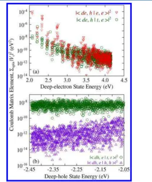
Figure 1b are similar to nonradiative Auger recombination processes in negative and positive trions, respectively.26 The recombination rates corresponding to these trapping processes are, however, much faster than those in trions. (Negative and positive trions have nonradiative lifetimes of ∼6 and ∼2 ns, respectively.26) To elucidate this further, we next present the Coulomb matrix elements (eq 1) for processes (i) and (iii) (|⟨de,h|Vc|t,e⟩|2and |⟨dh,e|Vc|t,t⟩|2) inFigure 2. We sum over all
spin-degenerate states and plot the resulting numbers as a function of final deep electronic state energy. For processes (i) and (iii), we compare these elements with those corresponding to nonradiative losses in negative and positive trions (|⟨de,h|Vc|
e,e⟩|2and |⟨dh,e|Vc|h,h⟩|2) inFigure 2a,b respectively.
We find that for shallow final electronic states the Coulomb elements associated with negative trions are up to four orders of magnitude larger than similar elements for the trapping process. However, these elements are never activated in trion because these transitions do not satisfy energy conservation. With an increase in final-state energy, both negative trion and trapping elements decrease and become comparable to each other. For trapping through shallow close-to-valence-band-edge traps via process (i), the relevant final-state energy lies close to the conduction band edge (∼2 eV in Figure 1b (i)). For nonradiative Auger recombination in negative trions, the relevant final states are at ∼4 eV. Therefore, as can be seen fromFigure 2a, even though for the same energy range negative trion Auger elements are up to four orders of magnitude larger than trapping elements, for energies relevant to trapping and nonradiative Auger in negative trions, the trend is reversed. The
trapping elements are up to four orders of magnitude larger than negative trion Auger elements.
We note that due to the sparse density of final electronic states close to the conduction band edge, the trapping through process (i) is strongly dependent on temperature and broadening which are required to bring the initial and final states into resonance.
For process (iii), due to strong overlap of trap state with conduction band edge and deep valence band states (both are delocalized over entire dot volume), trapping elements are up to four orders of magnitude larger than positive trion Auger elements. This results in up to four orders of magnitude faster trapping through process (iii) compared with nonradiative Auger recombination in positive trion.
Delocalized Outer-Surface Traps. Up to this point, we have
considered only strongly localized traps. In real CQDs, traps can be delocalized over many atoms, even if they originate from a point defects, such as a vacancy or an anion dimer.7To study the effect of delocalization on trapping rates, we considered three different traps on the outer surface with varying degrees of localization, as shown inFigure 3. The first trap is localized
over only a few atoms, the second trap is delocalized on the outermost atomic layer along the circumference of the shell, and the third trap is extended radially toward the core. We characterize the localization of these traps using the participation ratio (see Section S2 for definition), which is roughly equal to the number of atoms over which the trap is localized.
We find that the effect of delocalization is more pronounced on process (iii). In going from strongly localized trap to outer-surface delocalized trap (from (a) to (b) in Figure 3), the trapping lifetime corresponding to process (iii) increases by more than four orders of magnitude, while the increase is only one order of magnitude for process (i). This strong dependence of process (iii) is due to decreasing coupling between trap−trap states with delocalization. In going from outer-surface to radial traps (traps (b) and (c), respectively, in Figure 3), trapping rates through both processes increase by more than two orders of magnitude, suggesting that radial trap provides better overlap with the core.
Ef fect of Trap Depth on Trapping Rates. We next present the
effect of trap state energy on trapping lifetimes through processes (i) and (iii) for localized outer-surface traps inFigure 4a. We find that for process (i) the lifetimes oscillate with Figure 2. Coulomb matrix elements for trapping processes.
Comparison of Coulomb matrix elements for trapping processes with nonradiative Auger processes in negative and positive trions for (a) process (i) and (b) process (iii) ofFigure 1b. The elements are plotted as a function of final electronic state energies of |de⟩ and |dh⟩. The VBM is located at −0.16 eV.
Figure 3.Effect of trap delocalization on trapping lifetimes. Variation of trapping lifetimes with delocalization of traps for processes (i) and (iii). The delocalization of different traps is characterized by participation ratio, which is unity for localized traps and is equal to number of atoms for completely delocalized traps. All considered traps are located at 60 meV above the VBM.
changes in the trap energy due to a sparse density of final electronic states in the conduction band and due to two orders of magnitude variations in trapping elements with final state energy (Figure 2a). Overall, with an increase in the trap energy, the lifetimes increase due to poorer overlap between conduction band edge electron with the final-state electrons (as was shown inFigure 2a).
On the contrary, for process (iii), the lifetimes are initially insensitive to changes in the trap depth due to a high density of final states. They start to increase for deep traps when the final hole state localizes into the core and thus overlaps less with the trap. With an increase in trap energy beyond 1.1 eV (not shown in figure), there are no hole states available that can satisfy the energy conservation. As such, process (iii) becomes unavailable for electrons thermalized to the band edge and traps deeper than 1.1 eV (relative to the VBM).
Shell Thickness Dependence of Trapping Rates. To investigate
whether trapping can be suppressed, we considered the effect of shell thickness on the outer-surface trap processes (i) and (iii) fromFigure 1b and report the calculated variation of trapping lifetimes with shell thickness for a localized trap inFigure 4b. As expected, the trapping rate decreases for thicker shells due to increased spatial separation between the trap and electron/ hole states and thus reduced overlap. Importantly, we find that shell-thickness-dependence of trapping follows exponential dependence (dashed lines in Figure 4b), in contrast with power-law scaling of the core-only Auger rates.28,29 An extrapolation of the exponential fit suggests a trapping lifetime larger than 0.1 ns for the fastest process (iii) in a 6 nm “giant”
shell. We note that this extrapolated lifetime is for a highly localized trap and with delocalization, as discussed above (Figure 3), lifetimes corresponding to process (iii) increase by two to four orders of magnitude, thereby resulting in complete suppression of trapping through process (iii) for thick shell dots.
For trapping through process (i), while the lifetimes decrease by an order of magnitude for radially delocalized traps, the strong thickness dependence (four orders of magnitude increase in trapping lifetime as compared with fewer than two orders of magnitude for process (iii)) suggests the elimination of trapping for thick shell dots.
■
EXPERIMENTAL OBSERVATIONSWe next discuss two different experimental measurements in context of our findings.
Galland et al.30 used electrochemical charging and time-resolved photoluminescence emission measurements to meas-ure switching between dark and bright emission states (commonly referred to as blinking) in 3 nm thick shell CdSe/CdS CQDs. The authors found that dark states disappear with the application of external negative potential, thereby suggesting empty traps and their filling as the cause of their deactivation. The authors further observed the suppres-sion of dark states with the growth of thick shells.
We find that our simulations predict a trapping lifetime of 0.1 ns for realistically delocalized outer-surface localized empty trap through process (iii) in a 2 nm thick CdSe/CdS CQDs. With an increase in shell thickness, the lifetime for process (iii) increase to only at most 1 ns for 3 nm thick shell, still quite fast to be resolved in experiments. For comparison, lifetime increases to 160 ns for process (i). Furthermore, because process (iii) is through empty traps, it is suppressed upon the filling of traps or with a further increase in the shell thickness (Figure 1b).
Chen et al.31 developed a new synthesis method based on slow shell growth and found significantly suppressed blinking in 2.4 nm thick shell CdSe/CdS CQDs compared with previous literature reports. From our simulations, we find that for 2.5 nm shell CQDs, trapping processes through both filled and empty traps are fast (subnanosecond compared with ∼50 ns radiative lifetime) for outer-surface traps. Therefore, the observed suppression of blinking in compact shell CQDs is likely due to elimination of traps due to particular precursors used in shell synthesis rather than due to higher quality core−shell interface. We used atomistic simulations to study trapping of carriers in core−shell CdSe/CdS CQDs. We studied interface and outer-surface traps and found that both types are sufficiently fast to almost completely suppress the light emission. Only “giant” shells are capable of slowing down the outer-surface trap recombination, whereas bright emission from compact shells (2.5 nm)31should rather be attributed to a complete absence of traps.
Our findings are in line with the experimental observations that suggest the suppression of ultrafast picosecond trapping processes in electrochemically charged or n-doped CQDs by filling the traps with electrons.30 Similar to experimental findings, our results also suggest suppression of trapping in thick-shell CQDs.30
Overall, experimental observation of bright states suggests that a complete elimination of traps is physically achievable and that more robust passivation techniques can be developed if we Figure 4.Effect of trap depth and shell thickness on trapping lifetimes.
Variation of trapping lifetimes with (a) trap-energy and (b) shell thickness for processes (i) and (iii) through localized outer-surface traps. The trap energies are reported relative to the VBM. The dashed lines in panel b are exponential fits to the variation of lifetimes with shell thickness. For process (i), traps are located at an energy of Ep− Esabove the VBM, where Epand Esare energies of p and s electronic
states. For process (iii), considered traps are within 250 meV of the VBM.
The Journal of Physical Chemistry Letters Letter
DOI:10.1021/acs.jpclett.7b01503
J. Phys. Chem. Lett. 2017, 8, 3179−3184
understand and control better the dynamic changes in quantum dot environment.
■
ASSOCIATED CONTENT*
S Supporting InformationThe Supporting Information is available free of charge on the
ACS Publications websiteat DOI:10.1021/acs.jpclett.7b01503. Table S1: Variation of trapping lifetime for trapping through process (iii) for traps located at 60 meV above the VBM. Calculation of participation ratio. (PDF)
■
AUTHOR INFORMATION Corresponding Author *E-mail: [email protected]. ORCID Ankit Jain:0000-0001-8091-9129 Oleksandr Voznyy:0000-0002-8656-5074 Author Contributions∥A.J. and O.V. contributed equally to this work.
Notes
The authors declare no competing financial interest.
■
ACKNOWLEDGMENTSThis research is supported in part by the Natural Sciences and Engineering Research Council (NSERC) of Canada, by the Ontario Research Fund Research Excellence Program, and by the IBM Canada Research and Development Center. A.J. is supported by the IBM Canada Research and Development Center through the Southern Ontario Smart Computing Innovation Platform (SOSCIP) postdoctoral fellowship. The SOSCIP consortium is funded by the Ontario Government and the Federal Economic Development Agency for Southern Ontario. Computations were performed on the GPC super-computer at the SciNet HPC Consortium. SciNet is funded by the Canada Foundation for Innovation under the auspices of Compute Canada; the Government of Ontario; Ontario Research Fund - Research Excellence; and the University of Toronto. P.H. acknowledges support by the University of Ottawa Research Chair in Quantum Theory of Materials, Nanostructures and Devices. We acknowledge Pavel Frantsu-zov for fruitful discussions.
■
REFERENCES(1) Veilleux, V.; Lachance-Quirion, D.; Doré, K.; Landry, D.; Charette, P.; Allen, C. N. Strain-induced effects in colloidal quantum dots: lifetime measurements and blinking statistics. Nanotechnology 2010, 21, 134024.
(2) Minotto, A.; Todescato, F.; Fortunati, I.; Signorini, R.; Jasieniak, J. J.; Bozio, R. Role of Core-Shell Interfaces on Exciton Recombination in CdSe-Cd x Zn1-x S Quantum Dots. J. Phys. Chem. C 2014, 118, 24117−24126.
(3) Becerra, L. R.; Murray, C. B.; Griffin, R. G.; Bawendi, M. G. Investigation of the surface morphology of capped CdSe nano-crystallites by 31P nuclear magnetic resonance. J. Chem. Phys. 1994,
100, 3297.
(4) Kalyuzhny, G.; Murray, R. W. Ligand effects on optical properties of CdSe nanocrystals. J. Phys. Chem. B 2005, 109, 7012−7021.
(5) Sewall, S. L.; Cooney, R. R.; Anderson, K. E. H.; Dias, E. A.; Sagar, D. M.; Kambhampati, P. State-resolved studies of biexcitons and surface trapping dynamics in semiconductor quantum dots. J. Chem.
Phys. 2008, 129, 084701.
(6) Tyagi, P.; Cooney, R. R.; Sewall, S. L.; Sagar, D.; Saari, J. I.; Kambhampati, P. Controlling piezoelectric response in semiconductor
quantum dots via impulsive charge localization. Nano Lett. 2010, 10, 3062−3067.
(7) Voznyy, O.; Sargent, E. H. Atomistic Model of Fluorescence Intermittency of Colloidal Quantum Dots. Phys. Rev. Lett. 2014, 112, 157401.
(8) Coe, S.; Woo, W.-K.; Bawendi, M.; Bulović, V. Electro-luminescence from single monolayers of nanocrystals in molecular organic devices. Nature 2002, 420, 800−803.
(9) Caruge, J.; Halpert, J.; Wood, V.; Bulović, V.; Bawendi, M. Colloidal quantum-dot light-emitting diodes with metal-oxide charge transport layers. Nat. Photonics 2008, 2, 247−250.
(10) Anikeeva, P. O.; Halpert, J. E.; Bawendi, M. G.; Bulovic, V. Quantum dot light-emitting devices with electroluminescence tunable over the entire visible spectrum. Nano Lett. 2009, 9, 2532−2536.
(11) Klimov, V.; Mikhailovsky, A.; Xu, S.; Malko, A.; Hollingsworth, J.; Leatherdale, C.; Eisler, H.-J.; Bawendi, M. Optical gain and stimulated emission in nanocrystal quantum dots. Science 2000, 290, 314−317.
(12) Bruchez, M., Jr.; Moronne, M.; Gin, P.; Weiss, S.; Alivisatos, A. P. Semiconductor nanocrystals as fluorescent biological labels. Science 1998, 281, 2013−2016.
(13) Dahan, M.; Levi, S.; Luccardini, C.; Rostaing, P.; Riveau, B.; Triller, A. Diffusion dynamics of glycine receptors revealed by single-quantum dot tracking. Science 2003, 302, 442−445.
(14) Courty, S.; Luccardini, C.; Bellaiche, Y.; Cappello, G.; Dahan, M. Tracking individual kinesin motors in living cells using single quantum-dot imaging. Nano Lett. 2006, 6, 1491−1495.
(15) Howarth, M.; Liu, W.; Puthenveetil, S.; Zheng, Y.; Marshall, L. F.; Schmidt, M. M.; Wittrup, K. D.; Bawendi, M. G.; Ting, A. Y. Monovalent, reduced-size quantum dots for imaging receptors on living cells. Nat. Methods 2008, 5, 397−399.
(16) Zhao, J.; Nair, G.; Fisher, B. R.; Bawendi, M. G. Challenge to the Charging Model of Semiconductor-Nanocrystal Fluorescence Inter-mittency from Off-State Quantum Yields and Multiexciton Blinking.
Phys. Rev. Lett. 2010, 104, 157403.
(17) Gomez-Campos, F. M.; Califano, M. Hole surface trapping in CdSe nanocrystals: dynamics, rate fluctuations, and implications for blinking. Nano Lett. 2012, 12, 4508−4517.
(18) Efros, A. L.; Nesbitt, D. J. Origin and control of blinking in quantum dots. Nat. Nanotechnol. 2016, 11, 661−671.
(19) Trivedi, D. J.; Wang, L.; Prezhdo, O. V. Auger-Mediated Electron Relaxation Is Robust to Deep Hole Traps: Time-Domain Ab Initio Study of CdSe Quantum Dots. Nano Lett. 2015, 15, 2086−2091. (20) Dong, S.; Pal, S.; Lian, J.; Chan, Y.; Prezhdo, O. V.; Loh, Z.-H. Sub-Picosecond Auger-Mediated Hole-Trapping Dynamics in Colloi-dal CdSe/CdS Core/Shell Nanoplatelets. ACS Nano 2016, 10, 9370− 9378.
(21) Califano, M. Efficient Auger electron cooling in seemingly unfavorable configurations: Hole traps and electrochemical charging. J.
Phys. Chem. C 2008, 112, 8570−8574.
(22) Califano, M. Off-state quantum yields in the presence of surface trap states in cdse nanocrystals: The inadequacy of the charging model to explain blinking. J. Phys. Chem. C 2011, 115, 18051−18054.
(23) Califano, M.; Gomez-Campos, F. M. Universal Trapping Mechanism in Semiconductor Nanocrystals. Nano Lett. 2013, 13, 2047−2052.
(24) Korkusinski, M.; Voznyy, O.; Hawrylak, P. Fine structure and size dependence of exciton and biexciton optical spectra in CdSe nanocrystals. Phys. Rev. B: Condens. Matter Mater. Phys. 2010, 82, 245304.
(25) Korkusinski, M.; Voznyy, O.; Hawrylak, P. Theory of highly excited semiconductor nanostructures including Auger coupling: Exciton-biexciton mixing in CdSe nanocrystals. Phys. Rev. B: Condens.
Matter Mater. Phys. 2011, 84, 155327.
(26) Jain, A.; Voznyy, O.; Hoogland, S.; Korkusinski, M.; Hawrylak, P.; Sargent, E. H. Atomistic Design of CdSe/CdS Core-Shell Quantum Dots with Suppressed Auger Recombination. Nano Lett. 2016, 16, 6491−6496.
(27) Cohen-Tannoudji, C.; Dupont-Roc, J.; Grynberg, G.; Thickstun, P. Atom-Photon Interactions: Basic Processes and Applications; Wiley Online Library, 1992.
(28) Kobayashi, Y.; Udagawa, T.; Tamai, N. Carrier multiplication in CdTe quantum dots by single-photon timing spectroscopy. Chem. Lett. 2009, 38, 830−831.
(29) Robel, I.; Gresback, R.; Kortshagen, U.; Schaller, R. D.; Klimov, V. I. Universal size-dependent trend in Auger recombination in direct-gap and indirect-direct-gap semiconductor nanocrystals. Phys. Rev. Lett. 2009,
102, 177404.
(30) Galland, C.; Ghosh, Y.; Steinbrück, A.; Sykora, M.; Hollingsworth, J. A.; Klimov, V. I.; Htoon, H. Two types of luminescence blinking revealed by spectroelectrochemistry of single quantum dots. Nature 2011, 479, 203−207.
(31) Chen, O.; Zhao, J.; Chauhan, V. P.; Cui, J.; Wong, C.; Harris, D. K.; Wei, H.; Han, H.-S.; Fukumura, D.; Jain, R. K.; et al. Compact high-quality CdSe-CdS core-shell nanocrystals with narrow emission linewidths and suppressed blinking. Nat. Mater. 2013, 12, 445−451.
The Journal of Physical Chemistry Letters Letter
DOI:10.1021/acs.jpclett.7b01503
J. Phys. Chem. Lett. 2017, 8, 3179−3184