Publisher’s version / Version de l'éditeur:
Vous avez des questions? Nous pouvons vous aider. Pour communiquer directement avec un auteur, consultez la première page de la revue dans laquelle son article a été publié afin de trouver ses coordonnées. Si vous n’arrivez pas à les repérer, communiquez avec nous à [email protected].
Questions? Contact the NRC Publications Archive team at
[email protected]. If you wish to email the authors directly, please see the first page of the publication for their contact information.
https://publications-cnrc.canada.ca/fra/droits
L’accès à ce site Web et l’utilisation de son contenu sont assujettis aux conditions présentées dans le site LISEZ CES CONDITIONS ATTENTIVEMENT AVANT D’UTILISER CE SITE WEB.
Laser & Photonics Reviews, 13, 11, pp. 1-7, 2019-09-23
READ THESE TERMS AND CONDITIONS CAREFULLY BEFORE USING THIS WEBSITE. https://nrc-publications.canada.ca/eng/copyright
NRC Publications Archive Record / Notice des Archives des publications du CNRC :
https://nrc-publications.canada.ca/eng/view/object/?id=2e0713e8-670f-47e8-a1bd-e511300acb63
https://publications-cnrc.canada.ca/fra/voir/objet/?id=2e0713e8-670f-47e8-a1bd-e511300acb63
NRC Publications Archive
Archives des publications du CNRC
This publication could be one of several versions: author’s original, accepted manuscript or the publisher’s version. / La version de cette publication peut être l’une des suivantes : la version prépublication de l’auteur, la version acceptée du manuscrit ou la version de l’éditeur.
For the publisher’s version, please access the DOI link below./ Pour consulter la version de l’éditeur, utilisez le lien DOI ci-dessous.
https://doi.org/10.1002/lpor.201900172
Access and use of this website and the material on it are subject to the Terms and Conditions set forth at
An ultracompact GRIN
-lens-based spot size converter using
subwavelength grating metamaterials
Luque
-González, José Manuel; Halir, Robert; Wangüemert-Pérez, Juan
Gonzalo; De
-Oliva-Rubio, José; Schmid, Jens H.; Cheben, Pavel;
Graded-index materials offer virtually complete control over light propagation in integrated photonic chips but can be challenging to implement. Here, an anisotropic graded-index metamaterial, synthesized with fully etched silicon subwavelength structures, is proposed. Based on this material, a spot size converter that expands the transverse electric (TE) mode field profile from a 0.5 µm wide silicon wire waveguide to a 15 µm wide waveguide within a length of only 14 µm is designed. Measured insertion losses are below 1 dB in an unprecedented 130 nm bandwidth, limited by the measurement setup, with full 3D finite-difference time-domain (FDTD) simulations predicting a bandwidth in excess of 300 nm. Furthermore, the device is well suited to feed fiber-to-chip grating couplers, while requiring a footprint ten times smaller than conventional adiabatic tapers.
1. Introduction
Chip graded-index (GRIN) materials enable a plethora of differ-ent applications in optics such as light collimation,[1–3]waveguide crossings,[2] sharp multimode bends,[4,5]or invisibility cloaks.[6] Such materials can be implemented either through complex gray-scale lithography or by using subwavelength gratings (SWG). A subwavelength grating is a periodic dielectric structure with a pe-riod shorter than the wavelength propagating through it, thereby
J. M. Luque-González, Dr. R. Halir, Prof. J. G. Wangüemert-Pérez, Dr. J. de-Oliva-Rubio, Prof. Í. Molina-Fernández, Dr. A. Ortega-Moñux Departamento de Ingeniería de Comunicaciones, ETSI Telecomunicación Universidad de Málaga
Campus de Teatinos s/n, 29010 Málaga, Spain E-mail: [email protected]
Dr. J. H. Schmid, Dr. P. Cheben National Research Council Canada 1200 Montreal Road, Bldg. M50 Ottawa K1A 0R6, Canada
The ORCID identification number(s) for the author(s) of this article can be found under https://doi.org/10.1002/lpor.201900172 © 2019 The Authors. Published by WILEY-VCH Verlag GmbH & Co. KGaA, Weinheim. This is an open access article under the terms of the Creative Commons Attribution-NonCommercial-NoDerivs License, which permits use and distribution in any medium, provided the original work is properly cited, the use is non-commercial and no modifications or adaptations are made.
The copyright line for this article was changed on 13 November 2019 after original online publication.
DOI: 10.1002/lpor.201900172
enabling the synthesis of metamaterials with a controllable equivalent refractive index using a single lithographic etch step.[7] Uniform (non-graded) SWGs have been used to demonstrate many high-performance devices in the silicon-on-insulator (SOI) platform,[7,8]including integrated biosensors,[9,10] ultrabroad-band waveguide couplers,[11]and narrow-band Bragg filters[12,13] among others. The anisotropy of such uniform SWGs has recently been exploited to achieve advanced functionalities such as broad-band behavior,[14] control of evanescent fields,[15]and high-performance polariza-tion handling.[16–18]However, in graded-index metamaterials, the advantages of this intrinsic anisotropy remain unexplored.
In this work we demonstrate the use of an anisotropic SWG based GRIN material to implement an ultracompact, robust, and efficient spot size converter (Figure 1a). The GRIN pro-file is created by continuously changing the duty cycle (DC) of the SWG structure in the lateral direction (Figure 1b). We de-velop an anisotropic equivalent material model that shows that the anisotropy shortens the length of the device and enables a quick yet accurate way to design SWG based GRIN materials. Our lens achieves a spot-size conversion of the fundamental TE mode from a 0.5 µm wide silicon wire to a 15 µm wide waveg-uide in a total length of 14 µm, making it ten times shorter than a conventional taper. Compared to state-of-the-art spot-size converters[19–24]we achieve an unprecedented 130 nm bandwidth with measured insertion losses (IL) below 1 dB.
We furthermore show that the lens can be used to feed fiber-to-chip grating couplers from standard SOI waveguides with low losses. Indeed, the proposed GRIN lens SWG assisted spot size converter exhibits an exceptional combination of reduced foot-print and insertion losses, as well as large bandwidth and toler-ance to fabrication errors.
2. Implementing the Anisotropic GRIN
Metamaterial
In a conventional isotropic GRIN lens, the refractive index profile follows a parabolic distribution.[25]
nGRIN(x) = nmax √ 1− 𝛼2x2, 𝛼 = 1 wGRIN 2 √ 1− (n min nmax )2 (1)
www.advancedsciencenews.com www.lpr-journal.org
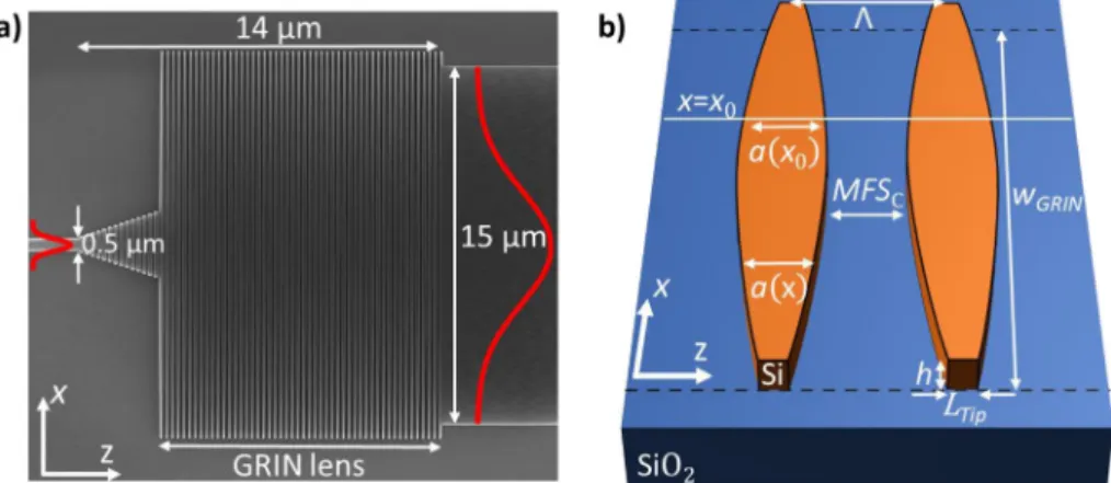
Figure 1. a) Scanning electron microscopy (SEM) image of the proposed spot size converter prior to the deposition of the SiO2cladding. The device
converts the guided mode of a conventional 500 nm wide silicon wire to the fundamental mode of a 15 µm wide waveguide, with insertion losses below 1 dB. b) Schematic of the subwavelength structure. The shape of the silicon blocksa(x) synthesizes the required index profile of the GRIN lens. The
silicon dioxide cladding is not shown for clarity.
wherenmaxandnminare the refractive index at the center and the edges of the lens,wGRINis the width of the lens, and𝛼 is a parame-ter which measures the curvature of the refractive index parabola. From a ray optics point of view, an isotropic GRIN lens collimates any paraxial input ray at a distancefRay= 𝜋∕2𝛼.[25]Therefore, the design of a compact GRIN-lens-based spot size converter mainly relies on increasing the curvature of the parabola,𝛼, to shorten the device length. However, the SWG structure exhibits an in-trinsic anisotropy,[16]so that the equivalent refractive index along thez-direction differs significantly from the equivalent refractive
index along thex-direction. As we will show later, this does not af-fect the device behavior, but significantly reduces its length when compared with the isotropic case. To take the anisotropy into ac-count, we estimate the collimation distance via electromagnetic analysis of the modes of the structure, considering the GRIN lens as a multimode gradual index waveguide. Specifically, the colli-mation distance can be expressed as[26]
fEM= L𝜋
2 =
𝜆0 4(neff 0− neff 1
) (2)
whereneff 0andneff 1are the effective indices of the fundamental and first order modes, respectively. It can be shown that the colli-mation distance is wavelength independent for a non-dispersive parabolic GRIN material.[26]
The design parameters of an SWG based GRIN lens are (see Figure 1b): i) the width of the multimode region,wGRIN, which enables us to reach the desired output beam width, ii) the shape of the silicon blocks,a(x) = DC(x)Λ, which implements the re-quired parabolic refractive index profile of the GRIN lens, and iii) the period of the structure,Λ, which optimizes the bandwidth behavior, as we will show later. First, we setwGRIN= 16 µm, only slightly wider than the desired output width to keep the curvature
𝛼 as high as possible. For periods large enough to be readily
fab-ricated, the device does not operate in the deep subwavelength regime, so that the shapea(x) which synthesizes the required re-fractive index profile depends on the period,Λ. Hence, both pa-rameters have to be designed simultaneously. We consider peri-ods in the range ofΛ = 180 nm to Λ = 180 nm to fulfil fabrication constraints and avoid Bragg reflections, respectively.
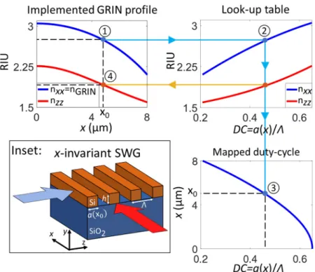
We now discuss the design process of the shapea(x) for an
intermediate period (Λ = 240 nm) and illustrate our anisotropic GRIN homogenization approach. We assume that the local equiv-alent refractive index at any position x0 along the GRIN lens (Figure 1b), is given by the equivalent refractive index of an
x-invariant SWG waveguide with the same duty cycle and period
(Figure 2: Inset). The core of this SWG structure can be ap-proximated by a homogeneous anisotropic uniaxial material with permittivity tensor 𝜺(DC) = diag[n2
xx(DC), n2yy(DC), n2zz(DC)][16]
which, for a given period, depends only on the duty cycle. There-fore, we can calculate a look-up table which maps a desired refractive index into its corresponding duty cycle as follows. First, we obtainnxx(DC) by computing the effective index of the
fundamentalx-polarized Floquet–Bloch mode propagating along thez-direction in the structure shown in the inset of Figure 2 (the
blue arrow indicates the propagation direction). The equivalent indexnxxis then given by the refractive index of a homogeneous isotropic slab waveguide whose fundamental TE mode has the same effective index as the Floquet–Bloch mode. Then, we obtain
nzz(DC), by proceeding analogously with the z-polarized Floquet
mode propagating along thex-axis (Figure 2: Inset, red arrow). For illustration purposes in this figure we assume a 220-nm-thick SOI platform at𝜆o= 1.55 µm and, referring to Figure 1b, a typ-ical tip widthLTip= 50 nm on the edge of the lens, and a MFSC of 80 nm in the center. Note that in the Supporting Informa-tion we demonstrate the proposed methodology for other silicon thicknesses. These values yield a duty cycle range fromDCmin=
LTip∕Λ ≈ 0.2 to DCmax= 1 − MFSC∕Λ ≈ 0.65, obtaining the look-up table relations shown in Figure 2. We then impose thatnxx(x)
follow the parabolic law in Equation (1) and use the look-up table to obtain both the shape of the silicon blocks,a (x) = DC(x)Λ, as
well as the value ofnzzimplemented by this duty cycle.
To validate our model, we compare 3D-FDTD simulations of the periodic lens structure (Figure 3a) with a homogenous anisotropic lens (Figure 3b) and a homogenous isotropic lens (Figure 3c), when they are illuminated by 3× 0.22 µm2(width by height) Gaussian beam. In the periodic lens structure the periods are shaped as determined by the algorithm presented in Figure 2. In Figure 3 we have indicated with a black dashed line the dis-tance where the beams have been fully expanded and collimated.
Figure 2. To implement the equivalent refractive indexnxx(x0)= nGRIN(x0) at any position x0, (marked as 1) we refer to a look-up table (marked as 2) constructed by analyzing
the structure shown in the inset, obtaining the shapea(x0) (marked as 3). This in turn
imposes the value ofnzz(x0) (marked as 4). Inset: Schematic of the periodic structure
used to calculate both polarizations of the look-up table. Typical SOI values,nSi= 3.476,
nSiO2= 1.444, h = 0.22 µm, and a period Λ = 0.24 µm are assumed. Three important conclusions can be drawn from Figure 3: i) the proposed structure works as a spot size converter (Figure 3a), ii) it can be accurately homogenized as an anisotropic graded-index metamaterial (compare Figure 3a,b), and iii) the isotropic homogenization does not emulate thez-periodic structure behav-ior (compare Figure 3a,c). Note that the formulafRay= 𝜋∕(2𝛼), with 𝛼 as defined in Equation (1), predicts a 17 µm collima-tion distance for the isotropic approach, close to the simulated isotropic value. Otherwise, by computing the effective indexes of the two lowest order modes of the gradual anisotropic waveg-uide (Figure 3b) and applying Equation (2), a 12 µm collima-tion distance is obtained, very close to the 11 µm of the periodic structure. Therefore, the anisotropic model can be used to de-sign the proposed GRIN lens with an anisotropic mode solver which is much faster than 3D-FDTD simulations. A similar anal-ysis to the one performed in Figure 3 has been carried out for the transverse magnetic (TM) mode in the Supporting Informa-tion, showing that the metamaterial still works as a spot size converter, but requires a longer device, since TM polarization does not benefit from the anisotropy mediated shortening of the collimation distance.[16]
3. Numerical Optimization of the GRIN Lens Spot
Size Converter
We now design the shape of the silicon blocks a(x) using the anisotropic model outlined in the previous section to seek
anisotropic GRIN model to calculate the modes of the multimode gradual index anisotropic wave-guide and then applying Equation (2) to esti-mate the collimation distance. Figure 4a reveals that the minimum collimation distance, marked with a dot for each period, is not achieved when the ratio nmax∕nmin is maximum (DCmax= 1 ⇒
MFSC= 0) as would be the case in an isotropic GRIN lens (see Equation (1)). This behavior is auspicious because it implies that the optimum
MFSC for a shorter device depends on the pe-riod and it is in the range of 50–90 nm. A flatter curve around the design point in Fig-ure 4a indicates that the device will be more tolerant to fabrication errors. We then calcu-late the wavelength dependence of the collima-tion distance assuming its optimum MFSC for each period (Figure 4b). Although longer periods imply a shorter collimation distance, the equivalent metamate-rial becomes more dispersive at shorter wavelengths, because of the proximity to the Bragg regime. The metamaterial dispersion changes the collimation distance as shown in Figure 4b, thereby detuning the device and increasing the insertion losses at short wavelengths. Therefore, from Figure 4a,b we conclude that the period should be set to 240 nm with a minimum feature size
MFSC≈ 80 nm in the center, achieving a flat dispersion behavior with a fabricable MFS. Finally, we refine the length of the GRIN lens via 3D-FDTD simulations, obtaining a final lens length of 10.5 µm, just 1 µm shorter than the anisotropic estimation. If we excite the designed z-periodic GRIN lens directly from the 0.5 µm width photonic wire waveguide (butt-coupling), the insertion loss of the device is about 2 dB at the central wavelength. To improve the lens performance, we have designed a short (15 periods long) input taper, as it is shown in Figure 1a. The role of this taper is twofold: i) To provide a smooth transition between the input silicon wire and the z-periodic structure, and ii) to ensure that the higher order modes of the lens are not excited. Note that the beam collimation condition of a GRIN lens requires the parax-ial approximation,[25]which is not satisfied for such higher order modes. To design the input taper we apply a two-step procedure: First, we determine, by using 3D-FDTD simulations, the min-imum length of the taper to assure negligible transition losses and back-reflections between the photonic wire at the input and the GRIN metamaterial. In this step, we keep the output taper width constant. Second, we optimize the output width of the ta-per to minimize the insertion loss of the whole device. With this
www.advancedsciencenews.com www.lpr-journal.org
Figure 3. Schematic of the structure (left) and real part of the 3D-FDTD simulated main component of the TE polarized electric field propagation,
e{Ex(x, z)}, along the proposed GRIN lens (right) implemented with: a) a z-periodic SWG structure, b) a gradual anisotropic material, and c) a gradual
isotropic material.
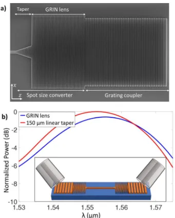
two-step approach, we achieve a reduction of the simulated in-sertion loss from 2 dB (butt-coupling) to 0.5 dB (with optimized adaptation taper). Final device dimensions are summarized in Table 1. In Figure 5a we show the simulated IL of the resulting spot size converter, achieving IL<1 dB in a bandwidth exceeding 300 nm.
4. Fabrication and Characterization
In order to experimentally demonstrate the proposed structure, a set of SWG GRIN lens spot size converters have been fabricated in a 220 nm thick SOI platform. The buried oxide (BOX) and the upper SiO2cladding are 2 µm and 2.2 µm thick, respectively.[27] The spot size converter has been fabricated with the nominal pa-rameters (Table 1) and±10% duty cycle offsets to study the tol-erances of the device. We included a set of back-to-back lenses cascaded multiple times to obtain the insertion loss of one GRIN lens (cutback configuration).
Light from a tunable laser (Agilent 81600B) connected to a lensed polarization maintaining fiber (PMF) is coupled into the chip using an SWG edge coupler.[28–30]The PMF is mounted on a rotatory stage, which, together with a Glan–Thompson polar-izer at the output allows us to control the polarization on the chip. At the chip output, light is focused onto a photodetector
(818-IR) using a microscope objective. The transmission spec-trum is measured by sweeping the wavelength of the tunable laser while recording the output power. Figure 5b shows the nor-malized measured output power at the central wavelength of the measured band (𝜆 = 1.58 µm) as a function of the number of cas-caded lenses. Insertion losses below 1 dB of are achieved even with a±10% offset in the duty cycle, indicating a good tolerance to fabrication deviations. As a reference, a conventional linear ta-per with a length of 150 µm exhibits comparable insertion losses of≈1 dB. Figure 5a draws the simulated (dashed blue line) and measured (solid blue line) insertion losses of the nominal SWG GRIN lens spot size converter. Spurious reflections have been re-moved using the minimum phase technique.[31]These measure-ments confirm that our device shows an excellent performance in terms of insertion losses, with IL< 0.6 dB at the central wave-length, maintaining the IL< 1 dB in a bandwidth from 1.51 to 1.64 µm limited by our setup, extending beyond 1.8 µm accord-ing to our simulations. In Table 2 we summarize the main char-acteristic of state-of-the-art spot-size-converters (SSC) in the SOI platform. To compare different expansion ratios, (ER= wout∕win), we use the normalized expansion ratio (NER).[23]
Figure 4. a) Collimation distance as a function of the gap in the
cen-ter of the lens (MFSC) calculated for different periods as obtained
through modal analysis of the homogenized anisotropic structure. Inset: Schematic of the period shape variation when changing theMFSC main-tainingwGRINandLTip. b) Collimation distance dispersion assuming the
optimumMFSCfor each period (marked with solid circles in Figure 4a).
Table 1. Geometrical parameters of the proposed spot-size converter.
GRIN lens wGRIN= 16 µm Λ = 240 nm
LTip= 50 nm a(x): see Figure 2
MFSC= 80 nm 44 periods
Input taper Λ = 240 nm DC= 0.65
wInTaper= 0.5 µm wOutTaper= 2.5 µm
15 periods
wherewoutandwinare the widths of the output and input waveg-uides,L is the length of the spot size converter, 𝜆 is the wave-length of the propagating light, and IL are the insertion losses (in linear scale). The first term of Equation (3), (ER), defines the expansion ratio normalized to the electrical length of the beam ex-pander. As a reference, for a Gaussian beam propagating through a homogeneous anisotropic material, this term can be calculated asER = 4⋅𝜆2⋅nxx
𝜋⋅w2 in⋅n2zz
. This expression can be considered as an upper limit for the NER of a beam expander (see Supporting Informa-tion). Our lens provides an excellent NER over an extremely broad bandwidth compared to the state-of-the-art.
As a further validation, we have used our spot size converter to feed a pair of grating couplers in a back-to-back configura-tion (Figure 6a,b: Inset). Note that opposed to beam expansion in a free space slab, which results in a curved phase-front and
Figure 5. a) Insertion losses as a function of the wavelength for the
nom-inal SWG lens design (blue lines). Measurements were performed using a back-to-back configuration, so measured insertion losses are divided by two. Our measurement setup is limited to the 1.51 µm< 𝜆 < 1.64 µm
wavelength range. b) Measured transmitted power as a function of the number of GRIN lenses at𝜆 = 1.58 µm Three different structures have
been characterized: the nominal design and two lenses with duty cycle off-sets of±10%, respectively.
Table 2. Performance of some state-of-the-art spot size converters.
Structure IL [dB] BW [nm] wout[µm] ER L [µm] NER [𝜆0] Ref.
Seg. taper <1a) N/A 2a) 4a) 1.5a) 3.7a) [19]
Lens assisted taper <1 80 10 22 21 1.32 [20] Seg. taper <1 50 12 24 20 1.86 [21] Adiabatic taper <1 N/A 12 24 150 0.24 [22] Semi lens <1 50 10 20 10 2.85 [23] Hollow taper 1.4a) 43a) 15a) 50a) 60a) 0.9a) [24]
This work <1 130 15 30 15 2.90 –
a)Simulation results.
thus requires specialized focusing grating couplers,[32] our spot sizes converter creates a flat phase-front and can therefore di-rectly replace an adiabatic taper. In this case, the measurement setup changes slightly: light from the laser is now coupled into a conventional SMF-28 fiber and the polarization is set to the desired TE state using a polarization controller (Agilent 8169A). Figure 6b compares the measured power when gratings are fed with a 150 µm linear taper and with our spot size converters. In terms of insertion losses the designed GRIN lens shows a behavior similar to a linear 150 µm long taper, even when cou-pling to a grating coupler that is specifically designed for the lat-ter. For the nominal GRIN lens, we observed comparatively high
www.advancedsciencenews.com www.lpr-journal.org
Figure 6. a) SEM image of the transition from a conventional 0.5 µm wide
silicon wire waveguide to a 15 µm wide grating coupler, through the SWG GRIN lens spot size converter. b) Measured wavelength response of a surface grating coupler fed with: a conventional 150 µm length linear ta-per (red line) and the SWG GRIN lens expander (blue line). The curves have been normalized to the maximum coupling efficiency of the red curve to facilitate the comparison. Inset: Schematic of the back-to-back grating coupler configuration, fed with a pair of the SWG GRIN lens spot size converters.
back-reflections of 14% due to the index mismatch between the lens and the grating. The back-reflections can be reduced by adding a properly designed transition between the GRIN lens and the grating coupler.[33]In this case, the+15% duty cycle offset GRIN lens yields a reduction of back-reflections to 8%, without significant impact on insertion losses.
5. Conclusion
We have reported a compact spot size converter based on an anisotropic GRIN lens based on an SWG metamaterial struc-ture. The proposed device expands a TE field profile 30 times over a distance of only 14 µm, with insertion loss under 1 dB in a measured bandwidth of 130 nm, while simulation predicts a bandwidth in excess of 300 nm. Compared with state-of-the-art devices, our lens achieves an excellent expansion ratio with out-standing bandwidth and is robust to fabrication errors. The de-vice has been utilized to feed a grating coupler with compelling results. Our anisotropic homogenization strategy enables fast yet accurate simulations of the GRIN metamaterial and we believe that it opens up promising new routes for on-chip light handling.
Supporting Information
Supporting Information is available from the Wiley Online Library or from the author.
Acknowledgements
The authors acknowledge funding from Universidad de Málaga, Ministerio de Economía y Competitividad (MINECO) (TEC2016-80718-R), Ministerio de Educación, Cultura y Deporte (MECD) (FPU16/06762), and Fondo Eu-ropeo de Desarrollo Regional—FEDER.
Conflict of Interest
The authors declare no conflict of interest.
Keywords
gradual index, integrated optics, metamaterials, spot-size converters, sub-wavelength gratings
Received: May 22, 2019 Revised: August 19, 2019 Published online: September 23, 2019
[1] U. Levy, M. Abashin, K. Ikeda, A. Krishnamoorthy, J. Cunningham, Y. Fainman,Phys. Rev. Lett. 2007, 98, 243901.
[2] Q. Wu, J. P. Turpin, D. H. Werner,Light: Sci. Appl. 2012, 1, e38.
[3] P. Lalanne, P. Chavel,Laser Photonics Rev. 2017, 11, 1600295.
[4] L. H. Gabrielli, D. Liu, S. G. Johnson, M. Lipson,Nat. Commun. 2012, 3, 1216.
[5] H. Xu, Y. Shi,Laser Photonics Rev. 2018, 12, 1700240.
[6] J. Li, J. B. Pendry,Phys. Rev. Lett. 2008, 101, 203901.
[7] P. Cheben, R. Halir, J. H. Schmid, H. A. Atwater, D. R. Smith,Nature
2018,560, 565.
[8] R. Halir, A. Ortega-Moñux, D. Benedikovic, G. Z. Mashanovich, J. G. Wangüemert-Pérez, J. H. Schmid, Í. Molina-Fernández, P. Cheben,
Proc. IEEE 2018, 106, 2144.
[9] J. Gonzalo Wangüemert-Pérez, P. Cheben, A. Ortega-Moñux, C. Alonso-Ramos, D. Pérez-Galacho, R. Halir, Í. Molina-Fernández, D. Xu, J. H. Schmid,Opt. Lett. 2014, 39, 4442.
[10] L. Torrijos-Morán, J. García-Rupérez,Opt. Express 2019, 27, 8168.
[11] H. Yun, L. Chrostowski, N. A. F. Jaeger,Opt. Lett. 2018, 43, 1935.
[12] J. ˇCtyroký, J. G. Wangüemert-Pérez, P. Kwiecien, J. Litvik, J. H. Schmid, Í. Molina-Fernández, A. Ortega-Moñux, M. Dado, P. Cheben,Opt. Ex-press 2018, 26, 3041.
[13] P. Cheben, J. ˇCtyroký, J. H. Schmid, S. Wang, J. Lapointe, J. G. Wangüemert-Pérez, Í. Molina-Fernández, A. Ortega-Moñux, R. Halir, D. Melati, D. Xu, S. Janz, M. Dado,Opt. Lett. 2019, 44, 1043.
[14] R. Halir, P. Cheben, J. M. Luque-González, J. D. Sarmiento-Merenguel, J. H. Schmid, G. Wangüemert-Pérez, D.-X. Xu, S. Wang, A. Ortega-Moñux, Í. Molina-Fernández,Laser Photonics Rev. 2016, 10,
1039.
[15] S. Jahani, S. Kim, J. Atkinson, J. C. Wirth, F. Kalhor, A. Al Noman, W. D. Newman, P. Shekhar, K. Han, V. Van, R. G. DeCorby, L. Chrostowski, M. Qi, Z. Jacob,Nat. Commun. 2018, 9, 1893.
[16] J. M. Luque-González, A. Herrero-Bermello, A. Ortega-Moñux, Í. Molina-Fernández, A. V. Velasco, P. Cheben, J. H. Schmid, S. Wang, R. Halir,Opt. Lett. 2018, 43, 4691.
Sons, New York 1991.
[26] S. El-Sabban, D. Khalil,Opt. Eng. 2015, 54, 037103.
Vakarin, G. Marcaud, X. Le Roux, E. Cassan, D. Marris-Morini, P. Cheben, F. Boeuf, C. Baudot, L. Vivien,Opt. Lett. 2017, 42, 3439.