Application of a Resonant Transmission Line Clock
Driver
by
Charles J. Cavazos
Submitted to the Department of Electrical Engineering
and Computer Science in partial fulfillment of the
require-ments for the degree of
Master of Engineering in Electrical Engineering and
Computer Science
at the
MASSACHUSETTS INSTITUTE OF TECHNOLOGY
May 21, 1999
@ Massachusetts Institute of Technology, 1999. All Rights Reserved.
A uthor ...
....
----. ...Charles J. Cavazos
May 21 1999
Certified by ... ...
TV
omas F.
ight, Jr.
Senior Research Scientist
7,Thesis
Supervisor
Accepted by ... ...
Arthur C. Smith
Chairman, Department Committee on Graduate Theses
MASSACH TE
Application of a Resonant Transmission Line Clock Driver
by
Charles J. Cavazos Submitted to the
Department of Electrical Engineering and Computer Science May 21, 1999
In Partial Fulfillment of the Requirements for the Degree of Master of Engineering in Electrical Engineering and Computer Science
Abstract
Power consumption is a major concern when designing a high performance microproces-sor. In conventional microprocessors, the clock distribution contributes to a major portion of the total power consumed. With the continuing trend of faster frequencies, higher com-plexity, and larger die sizes, clock distribution is quickly becoming one of the major issues faced by designers. A new solution to this problem is to use an external transmission line as a resonant clock driver. The two main advantages of this technique is its low power and no clock skew.
This paper describes the design of a 1 mm x 1 cm die along with its substrate that are com-bined via flip-chip bonding. The chip is designed to simulate a conventional clock load
and clock driver. The operating frequency for this design is 1 GHz. The total clock load is over 300 pF and the clock driver size is 6 cm. Discussed in detail are the circuits on-chip for functionality and skew measurements as well as the different substrate configurations for constructing a resonant transmission line.
Thesis Supervisor: Thomas F. Knight, Jr.
Table of Contents
1 Introduction...6 2 Theory ... 8 3 Chip Design ... 11 3.1 Clock Driver... 11 3.2 Functional Blocks ... 133.3 Tim ing Circuits ... 14
3.4 Pads ... 16 4 The Die...18 4.1 Power supplies ... 18 4.2 Clock ... 19 4.3 Functionality ... 20 4.4 Testability ... 21 5 Substrates ... 22 6 Testing...27 6.1 Skew measurements...27 6.2 Power measurements ... 29 7 Conclusion ... 30
List of Figures
Figure 2.1: Standard clock driver system. ... 8
Figure 2.2: Transmission line clock driver. ... 9
Figure 3.1: Chip design showing logic blocks...11
Figure 3.2: Clock driver schematic... 12
Figure 3.3: Schematic of type I flip-flop. ... 13
Figure 3.4: Schematic of type II flip-flop...13
Figure 3.5: Schematic of functional blocks. ... 14
Figure 3.6: Schematic and layout of arbiters. ... 16
Figure 3.7: Schematic of an 1/0 pad ... 17
Figure 4.1: Chip pad locations and labeling convention...18
Figure 4.2: Chip divided into functional sections with pad locations...20
Figure 5.1: Mesh configuration inside substrate for transmission line...23
Figure 5.2: Chip on substrate without transmission line. ... 23
Figure 5.3: Chip on substrate with transmission line... 24
Figure 5.4: Impedance variation in transmission line by signal shaping...24
Figure 5.5: Transmission line with veractors tapping along length...25
Figure 5.6: Side view of transmission line in substrate. ... 26
Figure 5.7: Sections of transmission line with connections in substrate. ... 26
List of Tables
Table 4.1: Pads dedicated for power supplies... 18
Table 4.2: Pads dedicated to clocking functionality... 19
Table 4.3: Pads dedicated for basic functionality. ... 20
Table 4.4: Pads dedicated for testability... 21
Chapter 1
Introduction
Power consumption is a major concern when designing a high performance micropro-cessor. In typical designs the clock distribution contributes a major portion of the total power consumed by a conventional microprocessor. The reason for this large power con-sumption is that the transition probability of a clock is 100% where as that of an ordinary logic signal is 33% on average. The percentage of total power consumed through the clock distribution can be as much as 40% as in the case of the Alpha 21164 microprocessor from Digital Equipment Corporation. With the continuing trend of faster frequencies, higher complexity, and larger die sizes, clock distribution and power consumption will become even more important.
Conventional methods to reduce the amount of power dissipated in microprocessors have their limitations. For example, a common approach is to reduce the power supply voltage since it results in a quadratic improvement. However, the power supply voltage can only be reduced so far until the propagation delay becomes too large for the desired frequency of operation or the noise margins become too small. The performance loss becomes even more significant when the power supply approaches the sum of the thres-hold voltages of the devices. By trying to save on the power consumed in clock distribu-tion, a considerable fraction of the total power can in turn be saved.
A new approach for reducing the power dissipation in clocking and producing sharp
transition time across an entire chip has been theorized by Matt Becker, a Ph.D. student at MIT. His technique revolves around an external transmission line that resonates the har-monics of a square wave to drive the clock net directly. The benefits of using a
transmis-translates to little or no skew and that the power consumed by clock distribution will be reduced. The power consumption in this method comes from the parasitic resistance of the transmission line which is considerably less than that burnt using conventional meth-ods.
For my thesis, I have designed a chip and substrate to produce experimental results of Matt Becker's theory. The chip is designed to simulate a conventional clock load and clock net. The fabricated chip includes circuits to test functionality as well as arbiters for on chip clock skew measurements. The substrate contains a transmission line tuned to res-onate at one GHz using Becker's impedance variation methods to support the first three odd harmonics of a square wave.
The following chapters contain an overview of the whole design process of the project. Chapter 2 describes the theory behind the resonant transmission line clock driver and how it saves power. Chapter 3 includes a hierarchical structure of the chip as well as design issues. Chapter 4 goes over the actual implementation of the design in the layout of the
die. Chapter 5 describes the various method in designing the substrate for this project.
Chapter 6 shows how to test the completed design to get the skew and power measure-ments.
Chapter 2
Theory
On a typical microprocessor, a generated clock signal is buffered through a several stages of inverters where the last stage inverter drives the clock load. The last stage inverter is usually fairly large in order to effectively drive the clock load. The interconnect of the clock lines can be lumped into a large RC network. Figure 2.1 shows a typical view of a standard clock driver. Most of the power dissipated in this clocking scheme is the con-stant charging and discharging of the RC network and pre-driver capacitances.
Clock Driver
Clock Load
Figure 2.1: Standard clock driver system.
In designing a clock distribution network there are several desired characteristics. For
one, there should be little to no clock skew from one side of the chip to the other. Also, the clock waveform throughout the chip should have sharp transition times. Common archi-tectures of a clock network are an H-tree structure or mesh design. The main advantage of the H-tree structure is that it minimizes the skew between clock nodes since all nodes are equally distant from the clock source.
To reduce the power consumed in distributing the clock, some architectures include turning off unused portions of the chip, a sleep-mode. This adds to the complexity of the chip design. Using a resonant transmission line as a clock driver, power is recovered by having the transmission line and not the clock driver charge and discharge the clock load. Since the transmission line is doing most of the work, the final stage clock driver can be
scaled down which adds to the power savings by reducing the pre-driver power. Figure 2.2
shows the setup for adding an external transmission line to drive the clock load on-chip.
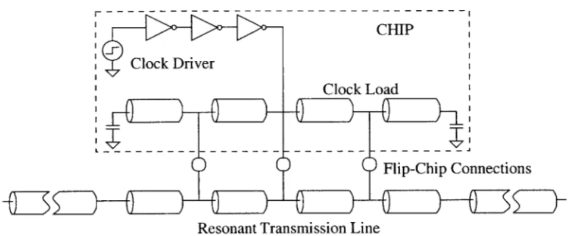
Clock Driver
Clock Load
Flip-Chip Connections
Resonant Transmission Line
Figure 2.2: Transmission line clock driver.
The theory behind this technique is as follows: The on-chip driver attempts to distrib-ute a square wave onto the clock load and the external transmission line. Since the driver is small and cannot drive the entire load, only a small pulse will travel down the transmis-sion line. The transmistransmis-sion line is open at the opposite end so that the pulse is fully reflected. The length of the transmission line is made so that when the pulse returns to the driver, it will coincide with the next pulse of the driver. This will result in a larger pulse height being sent back down the line. Eventually the transmission line will be resonating rail to rail at the given clock frequency. This model for the theory is not completely
accu-rate due to parasitics and impedance variations in the transmission line, but provides a conceptual view of the process.
Chapter 3
Chip Design
I --- rL--- ---
---Figure 3.1: Chip design showing logic blocks.
The design style of the chip is the Hewlett-Packard 0.35[t process fabricated through
MOSIS, a low cost prototyping and small-volume production service for VLSI circuit
development. A slice, 1 mm x 1 cm, of a full size chip is fabricated for cost reasons. The chip consists of four major logic blocks: a clock driver, functional blocks, arbiters, and pads. Figure 3.1 shows the chip divided into the main logic blocks.
- Clock driver: to drive the clock load along with the resonant transmission line in the
substrate.
- Functional blocks: to ensure that the chip is functioning correctly and provides
suffi-cient capacitance to simulate a typical chip.
- Timing circuits: to measure the clock skew between different points on the chip.
- Pads: clock, data, and power signals which will merge the chip to the substrate.
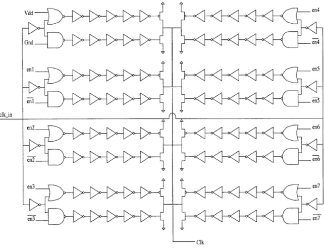
3.1 Clock Driver
An off chip crystal oscillator will feed a one Gigahertz signal onto the chip. This ref-erence clock signal (clk-in) is then sent to eight drivers through an H-tree structure to ensure the reference clock signal arrives at the same time to all the drivers. Each driver then buffers the reference clock signal through step up inverters at a factor sizing of four. Since this chip is one-tenth the size of the Alpha microprocessor which has a 60 cm inverter for its final clock driver, the last stage inverters are scaled accordingly. The last stage inverter of a single driver is one-eight the size of a 6 cm x 0.4 gm inverter so that
when all eight drivers are enabled, the clock driver would have a combined strength of a single 6 cm x 0.4 gm inverter. Figure 3.2 shows the schematic of all eight clock drivers.
Clk
Figure 3.2: Clock driver schematic.
Each of the eight drivers on the chip has its own enable signal; however one driver will always be on as shown in Figure 3.2. The other drivers will be activated according to the
decoding of the three bit control signal clk-en[0:2]. For example clken[0:2] = 000
repre-sents no addition drivers while clk-en[0:2] = 110 represents turning on six additional
driv-ers. This way the drive strength of the line clock driver can be stepped up or stepped down. It is expected that with a transmission line, fewer drivers will be needed to drive the
entire clock load effectively. The drivers on-chip have been designed in order to produce a
50% duty cycle clock waveform.
3.2 Functional Blocks
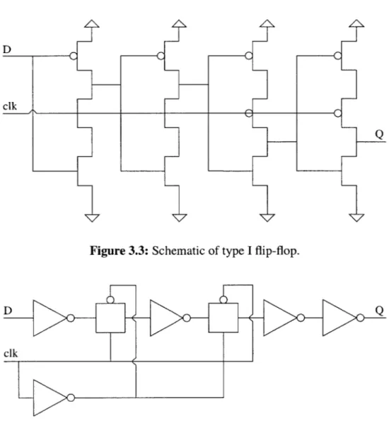
Figure 3.3: Schematic of type I flip-flop.
Figure 3.4: Schematic of type II flip-flop.
The entire functional blocks on the chip will consist of two types of latches. Two of the same type of latches are then combined to create an edge-triggered flop. The flip-flops are designed to have data dependent capacitances on the clock load. Figure 3.3 and
Figure 3.4 show the two different types of flip-flops used in this project. The total gate capacitance from the type I flip-flop seen by clk is 40 fF and the total gate capacitance from the type II flip-flop seen by clk is 27.7 fF. There are four main sections of flip-flops, each section containing about 2,200 flip-flops (4,400 latches), that are connected together in a scan chain. Half of all these flip-flops are made up from type I and half are made up from type II. The clock load due to just gate capacitance is roughly 300 pF.
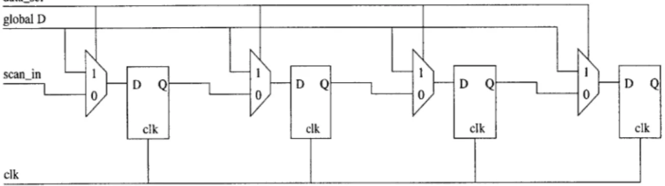
datasel global D scan-in 1I sainD Q D Q D Q D Q ck ck clk clk clk
Figure 3.5: Schematic of functional blocks.
The input to each latch has a mux in front of it. This is done so that the scan chain or the global data line common to all the flip-flops in that sector can be selected. Figure 3.5 shows a schematic of the functional blocks. The scan path will be used to test the func-tionality of the flip-flops. The global signal line will be used to see how the capacitance on the clock load can vary when the data signals are all ones or all zeros and switching from all ones to all zeros and vice versa.
3.3 Timing Circuits
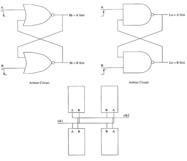
The timing circuits on the chip will consist of several strategically placed arbiters. An arbiter is a circuit which outputs which of two transitioning signals has occurred first. The
of interest are left end to right end, left end to middle, and middle to right end of the chip. Skew will be measured by comparing the arrival times of a test clock signal (TB) with that of the local clock signal. The TB signal is generated off chip and is a one Gigahertz square wave. Before entering the arbiter, the test clock signal goes through an external trombone delay circuit where the delay through that path is varied and can be precisely measured. The length of the delay will be varied until the order in which of the two clock signals arrives at the arbiter is switched. The test clock signal will be routed from the cen-ter of the chip to the arbicen-ters using an H-tree structure so as to reach all the arbicen-ters at the same time. The test clock signal is also shielded by ground lines from any cross coupling with data lines on the chip.
The arbiters are a cross connected NAND and NOR implementation. Two cross-cou-pled NAND gates make up a rising-edge arbiter where a low on either output represents which input transitioned from a high to low first. Similarly two cross-coupled NOR gates make up a falling-edge arbiter where a high on either output represents which input transi-tioned from a low to high first. Table 3.6 shows the schematics and layout of the arbiters.
The layout of the arbiters are mirrored side to side and then top to bottom to reduce any biasing of the input signals to the arbiter. The length of the devices making up the arbiters were increased by a factor of two for the NANDs and by one and a half for the NORs. This is to ensure that if there is a process variation from one end of the chip to the other, the precision of the arbiters would not be affected. The nwells and pwells of the arbiters are also isolated from the rest of the chip and powered independently in order to keep the sensitivity of the arbiters in tact.
Lo = A first
Hi = B first Lo = B first
B B
Arbiter Circuit Arbiter Circuit
A B B A
clk2 clk1
A B B A
Mirrored Arbiter Layout
Figure 3.6: Schematic and layout of arbiters.
3.4 Pads
Since this chip is connected to a substrate using flip-chip bumping, there is a grid array of flip-chip bumps for the data, control, clock, and power signals. The bump size of the pads are 125 jim and have a pitch of 250 Rm (center to center). They are also octagon in shape to aid in the bumping of the die.
There are four types of pads on the chip: vdd pads, gnd pads, clk pads, and I/O pads. The vdd pads are directly connected to the metal 4 vdd lines. The gnd pads are similarly
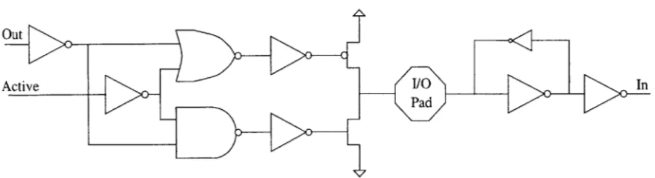
The 1/0 pads include some logic that supports either input mode or output mode.
Figure 3.7 shows the schematic of an
I/O
pads. If the I/O pad is an input pad, meaning the1/0 pad is driving the value of In, then the active signal is set low so the pmos and nmos
devices are both off. If the 1/0 pad is an output pad, then the active signal is set to high, so that the value of Out is driven onto the 1/0 pad.
Out
In
Chapter 4
The Die
The die contains 104 pads as show in Figure 4.1. The pads are laid out in three rows along the length of the die. Table A. 1 shows the breakdown of the pads to their function. The die is then connected to a custom built substrate via flip-chip connections.
C0o C39
BB20 0 0 0 00 0 00 0 0 0 0 0 00 0 00 OB21 E
nnn nnn nnn nnn nnn nnB 2 3
MB1[J _ - nnF1nnnnnn 00E l lF lE 1 1F 1nRF AO
Figure 4.1: Chip pad locations and labeling convention.
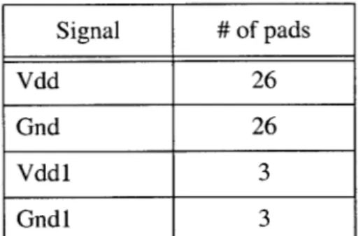
4.1 Power supplies
A39 Signal # of pads Vdd 26 Gnd 26 Vddl 3 Gndl 3Table 4.1: Pads dedicated for power supplies.
On the die there are two type of power supplies. One is vdd and gnd which powers all of the circuits on the die except for the arbiters. The arbiters have there own separate power supply, vddl and gndl. The need for separate power supplies for the arbiters as mentioned before is to isolate the arbiters from the rest of the chip and to reduce any noise due to power supply fluctuation.
The power pads are spread out evenly around the edge of the die in an alternating man-ner. The number of power pads was determined to be twice the number of constantly switching pads. Also, on the die there are many bypass capacitors placed between vdd and gnd, and between vddl and gndl, to further reduce any power supply fluctuations.
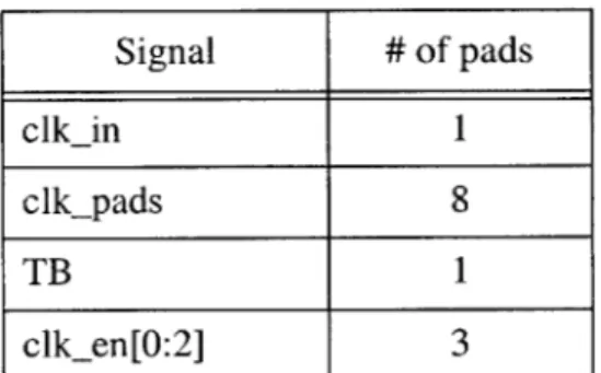
4.2 Clock
Signal # of pads clk-in 1 clk-pads 8 TB 1 clken[0:2] 3Table 4.2: Pads dedicated to clocking functionality.
In the layout of the die, the TB signal is very important. This is the test clock signal that is sent to all the arbiters on the die. The TB signal must reach all the arbiters at exactly the same time in order for the skew measurement tests to function accurately. The TB sig-nal is buffered through a few inverters and then distributed in an H-tree structure to reach all the arbiters. Every path from the TB signal to all the arbiters is exactly the same. Each paths has the same length, number of vias, turns, and capacitive loading. The TB signal is
also shielded with gnd lines running parallel to the TB signal throughout the die.
The clock distribution network is a mesh design. The eight clk-pads that are connected to the transmission line are laid down the length of the die and spaced evenly. The clock driver is located in the center of the die. There should be a considerable amount of skew without the transmission line, since the clock distribution network is a mesh and not an H-tree. With the transmission line, the skew should be reduced if not eliminated.
4.3 Functionality
Signal # of pads scanin[0:3] 4 scanout[0:3] 4 global-d[0:3] 4 datasel[0:3] 4Table 4.3: Pads dedicated for basic functionality.
DS 90 D D 2 D 3
Section 0 H H Section 1 Section 2 H I Section 3
SOo SOl S02 S03
Figure 4.2: Chip divided into functional sections with pad locations.
The chip is roughly divided into four major sections of chained edge-triggered latches. Each section has its own scanin (SI), scanout (SO), global-d (GD), and datasel (DS) as shown in Figure 4.2. The datasel controls whether the input to the flip-flops is either the globald value or the output of the previous flip-flop (the scan chain). For example if
DS 1=0 then all the flip-flops in section 1 will be set to receive inputs from their preceding
flip-flop, and if DS1=1 then all the flip-flops will be set to whatever value GD1 is set to. From scanin to scanout of any of the sections, the signal would travel through 2,200 flip-flops.
4.4 Testability
Signal # of pads arbsel 1 HA[0:2] 3 HB[0:2] 3 LA[0:2] 3 LB[0:3] 3Table 4.4: Pads dedicated for testability.
These signals are used in helping measure the on-chip skew of the chip's generated clock signal. Arbsel is used to select the outputs of either the arbiters with triggers at the
50% of Vdd or the arbiters with triggers at the 30% of Vdd. The two types of arbiters
measure the skew at different trigger points so that the slope as well as the skew of the clock can be determined. HA[0:2] and HB[0:2] are output signals where a high value on either signal indicates that its corresponding input's falling edge arrived first. A low on either LA[0:2] and LB[0:2] indicates its corresponding input's rising edge arrived first. The index zero corresponds to the left arbiters, an index of one corresponds to the center arbiters, and index of two corresponds to the right side arbiters.
Chapter
5
Substrates
For our purposes, the characteristics of the substrate are very important. Desired phys-ical characteristics include low impedance, multi-layered, ceramic, tungsten wires, and a high dielectric constant. The substrate is connected to the chip die via flip-chip bonding. The pads are connected to the substrate via flip-chip bumping and routed through the sub-strate to lead to pins. These pins are accessible to the outside and are used in the testing of the package.
Vdd and gnd signals are routed to pins near and around the chip. External bypass
capacitors are placed between the vdd and gnd pins to reduce power fluctuations. The I/O signals of the chip are routed to a central location near the end of the substrate so that they can be combined with a board for testing. Tapping into the clock routing will depend on the configuration method of the transmission line.
The transmission line is created using a mesh design of interleaving vdd/gnd and clk wires. The transmission line will take up most of the layers in the substrate. By routing clk and vdd/gnd in multiple layers and then connecting the lines in parallel, the impedance of the transmission line is reduced. Figure 5.1 shows how the transmission line will look inside the substrate.
yz
z
3 Clk
l Vdd/Gnd
Figure 5.1: Mesh configuration inside substrate for transmission line.
Figure 5.2: Chip on substrate without transmission line.
For our testing purpose, there are different configurations of the substrate on which a chip is attached. One is used as a benchmark comparison and has no transmission line in the substrate. It simply routes the input and outputs to their corresponding pins as shown
in Figure 5.2.
Other configurations will include some type of transmission line in the substrate.
Figure 5.3 shows a chip connected to a substrate containing a transmission line.
will
Figure 5.3: Chip on substrate with transmission line.
In this project, different ways to construct the transmission line are explored. One approach is using a shaped transmission line. Here the number of the clk signals in the transmission line is varied along the length of the transmission line in order to produce the
impedance variations needed for resonance of the first three odd harmonics. Figure 5.4
shows what this approach looks like in the substrate.
y
zo
Clk
Another method is building a regular transmission line using the mesh approach and tapping it along its length with varactors (variable capacitors). In this configuration the
impedance of the transmission line along its length can be adjusted externally. Figure 5.5
shows what this approach looks like in the substrate, where the pins have been omitted for clarity.
Figure 5.5: Transmission line with veractors tapping along length.
To connect the transmission line to the clk pads, special routing of the signal lines are
made so that the transmission line regularly connects to the clk pads on the die. Figure 5.6
shows a side view of how the signals are routed to make the connections. Figure 5.7
I I I I I I I I I I Chip
I
|m
1... 2.. 3.. 456 8. 9 10 .k... z C... d ..
ubstrate
1 2 3 4 567 8 910 z x ~Clk F,3VddGnd 11r 1/0
Figure 5.6: Side view of transmission line in substrate.
Connect to cilkpad
..
m....
HIT
1U
EUD
ID>
mm
Transmission line...
u.. l....
TO
EU EU0
DIP
Cross.connection Shifting of signals...
l. l...
.EUEU EU EU
I11I
[M1LORE110'
Shifting of sias Cross connections....
I
....
I
..
...
T ...
..
...
Figure 5.7: Sections of transmission line with connections in substrate.
Clk
Vdd/Gnd
I/O
Ay
Chapter 6
Testing
Inputs signals, with the exception of clk_in and TB, are connected to switches, driving either high or low. Clk_in and TB are generated from a crystal oscillator divided down to produce a one Gigahertz signal.
Input switches: - Clk_en[0:2] - Arbsel - Scanin[0:3] - Global_d[0:3] - Datasel[0:3]
All the output signals will be connected to an LED and pin. An 'on' LED represents a
high signal and an 'off' LED represents a low. The LEDs chosen will have there own sep-arate power supply so that the LEDs do not draw off power from the chip itself. The wave-forms on the output can be examined by connecting an oscilloscope to the output pins.
Output LEDs/pins: - Scanout[0:3] - HA[0:2] - HB[0:2] - LA[0:2] - LB[0:2]
6.1 Skew measurements
On the chip, there are arbiters that compare the arrival times of the clk signal and the TB signal. The clk signal enters all the arbiter as 'A' and the TB enters all the arbiters as 'B'. One of the values of HA[i] and HB[i] should be toggling while the other remains low.
on-chip clock arrived at the arbiter before the falling edge of TB signal. Similarly for the out-puts of LA[i] and LB [i]. One of the values of LA[i] and LB [i] should be toggling while the other remains high. The reason for the toggling of the output signal is due to the reseting of the arbiters. The resetting occurs at the frequency of the input signals which is one Gigahertz.
HA[0]
HB[0]
HA[2]
HB[2]
Figure 6.1: Example of a skew measurement.
To measure the skew the following steps are taken:
1. Pick which arbiters to use (arbsel=O selects the 50% arbiters and arbsel=1 selects the 30% arbiters).
2. Vary TB until the outputs of the selected arbiter switches from one to the other, or a metastability occurs. For example, if comparing the falling edges at left edge of the chip adjust TB until HA[0]=toggling and HB[0]=0 switches to HA[O]=0 and HB[0]=toggling or vice versa.
3. Record the time delay from the trombone delay (TI).
4. Vary TB until the outputs of the other arbiter switches from one to the other, or a metastability occurs.
5. Record the time delay from the trombone delay (T2).
6. The skew is then just the difference T2-T1.
The edge that is of concern is simply picked by observing the output pin that corre-sponds to that edge. Figure 6.1 shows a diagram on how the skew measurement is made.
6.2 Power measurements
Power measurements are done by measuring the current drawn from the power supply to the chip. These measurements are done on all the different substrate configurations. Here the inputs are kept the same from one substrate configuration to the next so that the current drawn from all the pads are the same in both cases.
For substrates that contain a transmission line, clk-en[0:2] can be adjusted to see what the minimum drive strength of the final stage clock driver can be with a transmission line
Chapter
7
Conclusion
Trying to reduce the amount of power consumed in the clocking of a chip is very desir-able for many reasons. The main reason being that the power dissipated by the clock is a significant portion of the total power dissipation of the chip. Another reason is that the transitional probability of the clock is one, where as other logic blocks switch a third of the time on average, so it makes sense to try to find ways to decrease the power consumed
by the clock.
In this paper, the design of a chip in order to simulate the clock load of a typical micro-processor has been described. A couple of the circuits on-chip should be noted. The imple-mentation of a variable strength clock driver is particularly useful for determining how well the resonant transmission line aids in driving the entire clock load. By varying the clock driver strength, the percentage of power saved with this technique can be deter-mined. The most difficult design and layout of the die were the arbiters. The sensitivity of the arbiters is very important in measuring the clock skew accurately, since traditional techniques for measuring clock skew off-chip are not possible due to the flip-chip bonding
of the die to the substrate.
Another difficult challenge was the design of the substrate. In order to construct a transmission line in the substrate, the substrate characteristics must be known and should be uniform over the entire substrate. The routing of the transmission lines in a multi-lay-ered substrate proves difficult when having to regularly cross connect the transmission lines as well as connecting to the pads on the die.
The design of the die has been fabricated; however, the design of the substrate config-urations has not yet been fabricated. Future work could refine the design of the substrate to produce a a transmission line that resonates at exactly one GHz.
Appendix A
Pin# Label Pin# Label Pin# Label Pin# Label
AO HA[O] A26 Gnd B12 clkpad C14 arbsel
Al Gnd A27 Vdd B13 DS[2] C15 Gnd
A2 HB[O] A28 SO[2] B14 GD[2] C16 LB[1]
A3 Vdd A29 Gnd B15 clk-pad C17 Vdd A4 Gnd A30 Vdd B16 Gnd C18 LA[l] A5 Vdd A31 SO[3] B17 Vdd C19 Gndl A6 Gnd A32 Gnd B18 clkpad C20 Vddl A7 Vdd A33 Vdd B19 DS[3] C21 LA[2] A8 SO[O] A34 Gnd B20 GD[3] C22 Gnd A9 Gnd A35 Vdd B21 clkpad C23 LB[2] A1O Vdd A36 Gnd B22 Vddl C24 Vdd
All SO[1] A37 HB[2] B23 Gndl C25 Gnd
A12 Gnd A38 Vdd CO LA[G] C26 Vdd
A13 Vdd A39 HA[2] Cl Vdd C27 Gnd
A14 clk en[0] BO Gndl C2 LB[O] C28 SI[2]
A15 Vdd B1 Vddl C3 Gnd C29 Vdd
A16 clk-en[l] B2 clk-pad C4 Vdd C30 Gnd
A17 Gnd B3 DS[O] C5 Gnd C31 SI[3]
A18 clkin B4 GD[0] C6 Vdd C32 Vdd
A19 Vddl B5 clkpad C7 Gnd C33 Gnd
A20 Gndl B6 Gnd C8 SI[0] C34 Vdd
A21 TB B7 Vdd C9 Vdd C35 Gnd
A22 Vdd B8 clkpad C1O Gnd C36 Vdd
A23 clk en[2] B9 DS[1] Cl SI[1] C37 LB[2]
A24 Gnd BIG GD[1] C12 Vdd C38 Gnd