Chirp Compensation in Active Mode-Locked Semiconductor Diode
Laser Using a DFB
by Susan Bach
Submitted to the
Department of Electrical Engineering and Computer Science in Partial Fulfillment of the Requirements for the
Degree of
Master of Engineering
at the
Massachusetts Institute of Technology
September 1994
© Massachusetts Institute of Technology, 1994. All rights reserved
Department of Electrical Engineering and Computer Science
_- September 14, 1994
Certified
by.
I / I IJ",-Hermann A. Haus
Institute Professor
Thesis SupervisorN
O\\
^A
AA-Accepted by
Chairman,
-$'~---' I ~" A '"Frederic R. MorgenthalerDepartrbital Committee on Graduate Studies
-.994
Author
_ ___I· __s___Y __
Chirp Compensation in Active Mode-Locked Semiconductor Diode
Laser Using a DFB
by Susan Bach
Submitted to the Department of Electrical Engineering and Computer Science on September 14, 1994 in Partial Fulfillment of the Requirements for the
Degree of Master of Engineering Abstract
This thesis investigates the possibility of canceling chirp in an actively mode-locked semiconductor laser using a DFB structure. The chirp is caused by the
nonlinearity of the diode, namely, the line-width enhancement factor, a. The
mode-locking equations are formed, and the postulated solution is a gaussian
pulse shape. The diode is modeled primarily using the rate equations for
carrier and photon densities, and the DFB is modeled by transfer matrix
theory. Using these models, a program was written to simulate a one-wayring structure. A mathematical analysis of the carrier density, given current
and pulse shape, enabled predictions on gain. From these results, the
mode-locking equations could be solved, thus defining the pulse uniquely and
determining the amount of dispersion necessary for no chirp. Once
dispersion was known, the DFB structure could be designed. First, numericalsimulations were run with no dispersion and a=O and also a=5. These
simulations demonstrated that the program works, and that a does produce a
significant amount of chirp. Following these results, simulations were run
with the DFB designed for three different amounts of dispersion:
Dfb=1.2662x10 2 5s2, 2.5332x10⁻² 6s2, and 7.1061x10⁻² 7s2. At Dfb=1.2662x10⁻² 5s2, where no chirp was calculated, there was very little -chirp, but double pulsing was a major problem. At Dfb=2.5332x10⁻²⁶s2, there was less double pulsing,
and the chirp seemed acceptably low. At Dfb=7.1061x10⁻² 7s2, there was quite a
bit of chirp, however the pulse was clean. It is suggested that the best among
the three is Dfb=2.5332x10⁻² 6s2 with K=250cm- 1 and a=5.Thesis Supervisor: Professor H. A. Haus Title: Institute Professor
Acknowledgements
First and foremost, I must thank Professor Haus. This project was his
creation and without his help it would have been impossible to complete.
His enthusiasm is heartening and contagious and sometimes it is just as
fascinating to watch him talk as it is to actually listen. He sets a standard forhonest and ambitious but friendy science which makes the Optics Group a
particularly pleasant and productive place to work.
Speaking of the lab, there are definitely others that I am grateful
towards. Luc and Farzana were amazingly patient and generous with their
time. Luc might be glad not to have me in the office 'assling him anymore,but I think he'll miss it! Farzana and I are "kindred spirits" (keep on
Trekkin!)--thanks for the computer expertise and good conversation. Other
people I would like to thank are Jerry, William, Gadi, Chris and, of course, Boris who was always willing to let me bend his ear.There are two people outside of lab whom I could just hug to death for
all their support and friendship. With friends like Audrey and Claudia, there
is nothing a person cannot do. This past year has been amazingly difficult
and you were there for me. Thank you, thank you, thank you!Finally, my family. To my brothers, Ralf and Jiirgen, you have been the best big brothers a little sister could ask for! I wish you both the best in your present endeavors. And to my parents, well, it is difficult to express so
much in words--"Gee, thanks!" just doesn't quite cut it.
Each day I
understand a little bit better just how much you have done for me and how
much you love me, and in learning this, each day I become stronger and more capable of returning that love to you and all those around me.PS I couldn't just leave without saying something about MIT as a whole. It has been a roller coaster ride through and through. The ups, the downs, the
good times and the bad times--I will remember everything like it was
yesterday. I am glad I took the ride, and I wish I'could take it again.Contents
1 Introduction 8
2 Mode-Locking 10
2.1 Introduction ... 10
2.2 Elements of Active Mode-Locking ... 11
2.2.1 Gain Medium ... 12
2.2.2 Linear Loss ... 14
2.2.3 Linear Phase Shift ... 14
2.2.4 Dispersion ... ... 14
2.2.5 Time Shift ... ... 14
2.3 Master Equation and Solution ... 15
2.4 Ring Structure ... 16 3 Semiconductor Lasers 17 3.1 Introduction ... 17 3.2 Gain ... 20 3.3 Rate Equations ... 21 3.4 Refractive Index ... 22
3.4.1 Propagation and Dispersion ... 23
3.4.2 Line-width Enhancement Factor ... 25
4 Distributed Feedback Structures 27 4.1 Introduction ... 27
4.2 DFB Equations ... 28
4.3 Dispersion ... : ... 30
4.4 Matching Structure ... 33
5 Simulation Models 37
5.1 Introdu ctio n ... 37
5.2 Simulating the Semiconductor Laser ... 37
5.3 Modeling the DFB ... ... 40 5.4 Combination Design ... 42 6 Mathematical Analysis 43 6.1 Introduction ... ... 43 6.2 Carrier Density ... ... 43 6.3 Mode-Locking ... 45 6.4 Design of the DFB ... ... 48 7 Results of Simulations 50 7.1 Introduction ... 50
7.2 Testing and Control Simulations ... 53
7.3 Results ... ... 57 8 Conclusion 62 8.1 Summary of Results ... 62 8.2 Analysis of Results ... 62 8.3 Possible Improvements ... 63 8.4 The End ... 63
A Calculating Parameters of the Pulse and DFB 64
B The Program 68
List of Figures
2.1 Resonant frequencies of the mode-locking cavity. Each mode has
some width due to nonlinearities and phase shifts within the
cavity. 11
2.2 Modulation of the gain and constant loss. 13
2.3 Ring model of mode-locked cavity. 16
3.1 Diagram of a semiconductor diode. 17
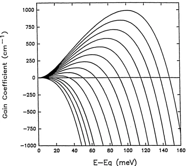
3.2 Picture of (a) spontaneous emission and (b) stimulated emission. 18 3.3. Total internal reflection occurs when nl>n2 and Oi>0c. 19 3.4 Gain of the diode over frequency for different carrier densities.
The gain increases with increasing carrier density. [1] 21
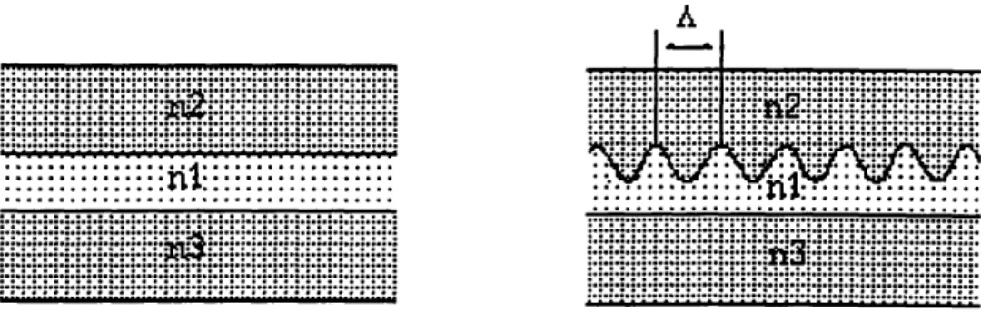
4.1 A normal waveguide and a DFB structure with sinusoidal
perturbations with period A.
28
4.2 Second-order dispersion versus 161 for lc=160 to 400cm-1. 31 4.3 Third-order dispersion versus 161 for ic=160 to 400cm- 1. 31 4.4 Ratio of third- to second-order dispersion for 5, 10, and 15ps pulses. 32 4.5 Plot of both positive and negative propagation constants, I, versus
8. The area in the middle is the stop band where P is imaginary. 32
4.6 Matching structure. 33
4.7 Smith chart model following r of the matched DFB structure. 34 5.1 Model of diode used for simulations. The diode is divided into
sections, each with an independent carrier density, and has field
arrays in between. 39
5.2 Modeling the DFB as a two-port system. 40
7.1 Output of the diode. The dashed line is the original pulse, and the
solid line is the output with current above threshold. 51 7.2 Output of the DFB structure: solid line is the input pulse, dashed
line is the field that traveled through, and dotted is the reflected
field. 51
7.3 Output of simulation with a non-bandlimited diode. 52
7.4 Output of simulation with bandlimiting.
52
7.6 Frequency spectrum of a single pulse from the above series. 54 7.7 A single pulse from the simulation with both DFB and alpha off. 54
7.8 Phase of the above pulse. 54
7.9 Series of pulses from simulation with alpha off and DFB on. 55
7.10 Section of above series one roundtrip in length. 55
7.11 Phase corresponding to Figure 7.10. 55
7.12 Series of pulses from simulation with DFB off and alpha on.
Sinusoidal line is relative carrier density (not actual values). 56 7.13 Frequency spectrum of a single pulse from the above series. 56 7.14 Single pulse from simulation with DFB off and alpha on. 56
7.15 Phase corresponding to Figure 7.14. 56
7.16 Series of pulses from simulation with Dfb=1.2662x10⁻² 5 and a=5. Sinusoidal line is relative carrier density (not actual values). 58 7.17 Frequency spectrum of a single pulse from the above series. 58 7.18 Single pulse from simulation with Dfb=1.2662x10⁻² 5 and a=5. 58
7.19 Phase corresponding to Figure 7.18. 58
7.20 Series of pulses from simulation with Dfb=2.5332x10⁻² 6 and a=5. Sinusoidal line is relative carrier density (not actual values). 60 7.21 Frequency spectrum of a single pulse from the above series. 60 7.22 Single pulse from simulation with Dfb=2.5332x10⁻² 6 and a=5. 60
7.23 Phase corresponding to Figure 7.22. 60
7.24 Series of pulses from simulation with Dfb=7.1061x10⁻² 7 and a=5. Sinusoidal line is relative carrier density (not actual values). 61 7.25 Frequency spectrum of a single pulse from the above series. 61 7.26 Single pulse from simulation with Dfb=7.1061x10⁻² 7 and a=5. 61
7.27 Phase corresponding to Figure 7.26. 61
List of Tables
3.1 Typical parameter values for a 1.3 gm diode laser from [3] 19
4.1 Signs of propagation parameters in the four quadrants as referred
to in Figure 4.5. 33
Chapter 1
Introduction
Semiconductor lasers were first realized in 1962. Their small size,
around 300gm, high power, and ease of mass production have made them
popular for such uses as CD players and pointers. However, in the case ofcommunication applications, especially in producing ultrashort pulses,
semiconductor lasers have undesirable nonlinear characteristics due to
changes in the carrier population and frequency dependent gain. These
factors cause pulse distortion, cross talk and limit the speed of propagation. [1]When using semiconductor lasers for mode-locking purposes, the cavity
must be designed for their nonlinearities.One undesirable effect of the nonlinearities in diode lasers is a chirped pulse. In this thesis, the use of a distributed feedback structure (DFB) to
suppress the chirp of mode-locked pulses will be demonstrated through
computer simulation. DFB structures are often usetas filters since they have a stop band, however in this case the pass band is being used to manipulate the pulse through dispersion. When mode-locking semiconductor lasers, acertain amount of dispersion in the resonating cavity will prevent the
presence of chirp in the steady state pulse. Often, optical fiber is used as thecavity, and the length of the fiber determines the amount of dispersion
within the cavity. Some examples show lengths of up to 50 meters. A DFB can do the same thing in one centimeter on a semiconductor chip. There are many advantages to this over using fiber. First, the DFB structure can be fabricated with the diode laser, and second, less energy is lost than would be from focusing the field into the fiber.The major concern in designing the DFB is the linewidth
enhancement factor, or the ca parameter, of the diode laser which causes the index of the material to change with gain, hence chirping. Chapters 2 and 3,which cover mode-locking and semiconductor diode lasers, respectively,
provide the background knowledge to determine how much dispersion is
needed to create a stable non-chirped pulse.Chapter 4 explains the theory on DFB structures, and from this
information in addition to the previous chapters, the DFB can be designed. It will also discuss a special use of DFB's to minimize the amount of reflections.Computer simulation will be implemented in order to test the above theories and demonstrate graphically a mode-locked pulse resulting from this design. Chapter 5 describes how each part of the diode and DFB is simulated
and implemented.
Chapter 6 contains a mathematical analysis of a diode laser, namely the
carrier density, to determine the amount of dispersion necessary. These
results will determine the values of the parameters of the DFB structure.Chapter 7 details the results of these simulations.
Finally, Chapter 8 includes a summary of the results will be given and
any explanations or further insights. Possible improvements and future
developments will be described as well.Chapter 2
Mode-locking
2.1 Introduction
Mode-locking is the method used to generate short pulses on the order of picoseconds or even femtoseconds in length. As the name implies, the phases of cavity modes are locked with respect to each other so that the sum of the modes renders a pulse usually of gaussian or sech shape. These pulses are used for communication, spectroscopy, etc. There are many approaches and tricks employed to create a mode-locking situation depending on what kind of laser is used and the set-up designed around it. Normally, the goal is to produce a pulse as short as possible with no chirp.
As mentioned above, a mode-locking cavity only supports the resonant frequencies, or modes of the cavity. The frequencies that exist within the cavity are dependent on the length of the cavity. In this case, length is not
just the physical length but also depends on the refractive index of the
materials within the cavity and is so called the optical length. The higher the index the slower the field propagates through the medium, thus the optical length is larger. The propagation constant of a wave for a linear medium is found from:P=o0n/c (2.1)
The following equation is equivalent to traveling with the wave:
wt-z=O (2.2)
where z is distance. From (2.2), a cavity of length L has an effective length of nL. For a frequency to exist within the cavity, the optical length must be a multiple of half wavelengths in the medium.
A =nL (2.3) 2
So the modes in the cavity have frequencies of:
c mc c
fm= _ = c and Af =- (2.4)
A 2nL 2nL
where m is the mode number. Because the cavity is composed of different media, the refractive index will not be constant throughout the cavity. Thus
it is easier to express the mode spacing, Axo, as 2/TR where TR is the
roundtrip time of the cavity.Ideally, there should be an impulse in the frequency spectrum for each mode at the appropriate frequency, however, realistically, the mode always has some width meaning that there is some energy in the frequencies close to the modal frequencies (Figure 2.1). This is due to noise.
mC(
f
Figure 2.1. Resonant frequencies of the mode-locking cavity. Each mode has
some width due to nonlinearities and phase shifts within the cavity.
Future figures of frequency spectrums may not show the individual
modes but only an envelope. In a mode-locking situation, these modes sum up to form a pulse in the time domain, the shape of which is dependent on the effect of all the components within the cavity on each mode.2.2 Elements of Active Mode-Locking
This section will explain all the parts of the master equation for active mode-locking. There are two approaches to analyzing and finding a solution
for a mode-locking equation, frequency and time. Mode-locking has both
frequency and time dependent parts, but it is generally easier to understand in the time domain. It is also easier to find a solution in the time domainbecause the equation corresponds to the one-dimensional Schroedinger
equation of a particle in a potential well [2]. Thus the known solutions to this equation can also be used for mode-locking.The effect of each element within the cavity is slight. If exponential,
the exponent with a small argument can be expanded and approximated in
time as:x2 X3
ex =
1 +
x + 2 + M+...= 1 + x (2.5)2! 3!
Following is a descriptive list each element required for mode-locking already in the form of "x".
2.2.1 Gain Medium
The main active mode-locking element is the gain. In semiconductor diodes, the gain is determined mostly by the injection current. More current means higher gain. Other lasers obtain energy from pump lasers--the more
intensity the pump laser provides the higher the gain of the mode-locked
laser. In either case, modulating the power source will cause modulation of the gain at the same frequency. For diode lasers, the relation between current and gain is linear but delayed, thus the peak of the current and the peak of thegain (or rather carrier density) do not coincide. The current should be
modulated around some threshold value above which there is net gain and below which there is absorption (Figure 2.2). The modulation frequency, 0m,of the current should correspond to the roundtrip time of the cavity, ie
should be equal to the mode spacing 27t/TR, in order to drive the adjacentmodes.
The gain, however, is also frequency dependent, and can be modeled with a lorenzian shape:
g(o)= go (2.6)
where go is the small signal gain at the center frequency and cog is the linewidth of the gain. The center frequency of the field within a mode-locking cavity is the resonant frequency closest to the center frequency of the gain medium. The above equation can be approximated as:
g(eo) = go(1- co-O ) (2.7)
and in the time domain this becomes:
d 2 (2.8)
Gai n
t
Figure 2.2. Modulation of the gain and constant loss.
The effect of the gain is expressed as:
G(t) = go(M(t) + 2 d-J (2.9)
where M(t) is the modulation of the gain.
Another gain related element necessary for mode-locking is saturation
of the gain. The presence of photons depletes the carrier density, thus
increasing intensity decreases the gain. In the initial transient state, the
intensity of the pulse increases until enough saturation occurs to achieve
steady-state. The relaxation time of the gain medium should be short enough for it to recover within the roundtrip time. The effect of saturation is expressed as:-S(t) (2.10)
Semiconductor lasers are unique in that they have a nonlinearity due
to the linewidth enhancement factor, a (also to be further explained in
chapter 2). It is a gain dependent factor in which the index changes with gain.ja(G(t) - S(t)) (2.11) This element creates difficulties in mode-locking because it induces chirping and instability. When designing the mode-locking cavity, it is important to consider this factor and to counter it with another element such as dispersion.
Another frequency dependent factor is dispersion. The gain medium
may have a negligible amount of dispersion compared to the amount
experienced within the rest of the cavity, but it is mentioned here since it isincluded in future calculation and because it does exist. The effect of
dispersion, which will be explained in greater detail in Chapter 2, is given by:-jDd(o.)2 2 (2.12)
-jDd(o - o)22 jD dt 2 (2.12)
r-\ n n n
A A
where Dd is half the second-derivative of the propagation constant times the length of the diode.
2.2.2 Linear Loss
Somewhere in the cavity the optical field will experience a linear loss, -L. The cause of this would be the output coupler, and also loss occurs when the field travels from one medium to another. Possibly, the medium itself will have some amount of loss.
2.2.3 Linear Phase Shift
In the steady state, the pulse after one round trip should be the same as it was before. However, there will be a difference in phase since propagation through a medium adds a phase shift. This is acceptable as long as the difference remains constant between consecutive pulses. The phase shift, j, has no shaping effect on the pulse, and only occurs as a result of satisfying the requirements for steady-state.
2.2.4 Dispersion
Dispersion in the diode was already mentioned, but there is also a
significant amount of dispersion in the rest of the cavity. Actually, in this case there has to be to compensate for the nonlinearity in the diode. The object of this thesis is to design a DFB structure with the right amount ofdispersion to prevent pulse-spreading and chirping caused by the diode. The
DFB dispersion is expressed as:
d2
-jD(o- o) jDj 2 dt2 _ (2.13)
where Dfb is half the second deriviative of the DFB propagation constant time the length of the DFB.
2.2.5 Time Shift
As the pulse travels through the diode, it experiences a pushing effect
causing delay or advancement depending on where the peak of the pulse is
with respect to the peak of the gain. So, if the peak of the pulse comes after the peak of gain, the pulse will be "pushed" ahead in time because the front part of the pulse experiences more gain than the later part. This effect is represented by:STd (2.14)
dt
That concludes the elements of mode-locking. The next step is to formulate a master equation which will define the pulse.
2.3 Master Equation and Solution
The previous section described every single effect experienced by the pulse in one round trip. The total effect can be expressed in a single equation:
d d2 d2
aexp(ST + jT) = aexp((G(t) - S(t))(1 + ja) - L +jDd + jD dt2 (2.15) where a is the pulse envelope. Both sides of (2.15) represent the pulse after one round trip. (2.15) can be simplified using (2.5):
d d2 d2
AT d + jT = (G(t) - S(t))(I + ja) - L +jDd + jD dt2 (2.16)
dt dt2
The ansatz for this equation is a gaussian shaped pulse:
a =IAIexp 2 ( + Jic) exp(-iAt) (2.17) where I A I is the amplitude, determines the pulse width, 3
c
is the chirpparameter, and Aco is the frequency shift. Applying this solution to (2.16) and separating it into parts by powers of t should render six real equations. For a given cavity, the unknowns of the master equations are the pulse parameters of eq (2.17) as well as W and T. Thus with six unknowns and six equations, the pulse can be defined uniquely.
In chapter 6, the six equations will be worked out explicitly once an analytical model of the gain has been written.
2.4 Ring Structure
This thesis will simulate a ring structure. In this model, Figure 2.3, the field travels only in one direction and passes through each medium once in one round trip. To insure that the field propagates only in one direction, an
isolator is modelled just before the diode. This isolator passes any field
travelling in the clockwise direction and absorbs any field propagating in the opposite direction. Of course, this is pretty idealistic, but any loss from the isolator can be included in the linear loss term above. However, isolators today are pretty good in absorbing the counter propagating fields so this model is not far from reality.I
Figure 2.3. Ring model of mode-locked cavity.
This does not mean there will be no counter-propagating waves. The
field will be partially reflected by the DFB structure causing backward
propagating waves to travel through the diode even with the matching
structure to be described in Chapter 4. If the amplitude of these waves issignificant, they will deplete the gain medium. This effect must also be
included when simulating the diode.
The ring model overall is much easier to simulate than a cavity
structure in which the field is reflected back and forth and experiences each effect twice as much but at different times. Also, when fields travel in bothdirections in the diode, standing waves form, causing spatial hole burning,
and some parts of the diode are completely depleted of carriers. This
phenomenon is rather difficult to simulate and is a under great deal of study--i.e. too much to think about here.Chapter 3
Semiconductor Lasers
3.1 Introduction
Semiconductor lasers are made by laying a p-type semiconductor
material on an n-type material. At the boundary of the two layers, the p-n
junction, electrons diffuse a short distance into the p side from the n side, and holes diffuse into the n side from the p side. The diffusion process reaches asteady state when the resulting charged donors on either side form a field
resisting further change in hole/electron populations. Applying a positive
voltage across the p-n junction, or forward biasing the diode, will weaken this field allowing more electrons and holes to diffuse into the area around the p-n jup-nctiop-n. This area, where both electrop-ns ap-nd holes exist p-near the jup-nctiop-n, is called the active region and is the most interesting part of the diode since it is where the optical field travels and experiences gain and loss.Recombination of the electron and holes in the active region results in
an emission of radiative or nonradiative energy. Radiative energy is in the form of photons whose frequency must satisfy the condition: hv=Eg, where Eg-1 - ---- -I -I electroues i
K
.
21
*-.--
p-typel
active region4
-
n-type
Figure 3.1. Diagram of a semiconductor diode.
n-electrons electrons
I ~
TAEg
holes holes
(a) (b)
Figure 3.2. Picture of (a) spontaneous emission and (b) stimulated emission.
is the gap energy emitted. The upper energy state of a free electron is called the conduction band while the lower state of a recombined electron/hole pair is the valence band. Eg is the difference in energy between these two states. A recombined electron/hole pair can also absorb this amount of energy and free the electron.
As stated before, forward biasing the diode increases the number of
electrons and holes diffusing into the active region. There is a threshold value for the voltage beyond which there is population inversion. The result is the rate of recombination is higher than the reverse process which meansthat there is more emission than absorption.
Thus the optical field
experiences gain.Photon emission from recombination is either spontaneous or
stimulated. A spontaneous emission occurs when an electron randomly
decays from the conduction band to the valence band, releasing energy.
Stimulated emission occurs when another photon induces the electron to
decay and release another photon. The photon radiated by the stimulated
emission will match the first photon in frequency and direction. Thus the light emitted by the laser will be mostly coherent.The active region is so designed that its refractive index is slightly higher than that of the surrounding p- or n-type material. Thus, the active region of the diode laser acts like a waveguide, one with gain and absorbtion, and the light is contained. The mechanism of containment begins with the difference in index. Because the index of the active region is higher, total
internal reflection occurs if the field hits the boundary with an angle of
incidence greater than the critical angle given by Snell's Law. The criticalnl
Figure 3.3. Total internal reflection occurs when nl>n2 and i>0c.
angle, 0c, of angle, is > 1.
the incident wave, i, is such that sinOt, the tranmitted field
(nl is the index of the active region; n2 is the index outside.)-sin Oi = 2 sin 0, Oc = sin n2
C C 1th (.1
The energy of any field traveling almost parallel to the edge region will be totally reflected.
of the active
Table 3.1 Typical parameter values for a 1.3 gm diode laser from [3]
Parameter Svmbol Value
Cavity length
Active-region width
Active-layer thickness Confinement factor Effective mode index Group refractive inexLine-width enhancement factor
Facet lossInternal loss
Gain constant
Carrier density at transparency
Nonradiative recombination rate
Radiative recombination coeff Auger recombination coeffThreshold carrier population
Threshold current
Carrier lifetime at threshold
Photon lifetime
L w dr
Cga
amaint
goNt
Anr B CNth
Ith Te V 250gm2gm
0.2gm
0.3 3.4 4 5 45 cm- 1 40 cm-l 2.5x10⁻¹⁶ cm2 1x101 8 cm-3 lx10 8 s-1 1x10⁻¹⁰ cm3/s 3x10- 2 9 cm6/s 2.14x10⁸ 15.8 mA 2.2 ns 1.6 psTable 3.1 lists the important parameters of a semiconductor diode and
their characteristic values. These are the actual values used for simulations
on the computer.
3.2 Gain
As stated earlier, the field experiences gain when an electron decays from an upper state to a lower state, imparting another photon to the field. If the density of electrons in the conduction band is high and the density of holes in the valence band is also high, then the field will see a net gain since the probablility of a stimulated emission is higher than that of a stimulated absorption. Conversely, if the density of the valence band is higher, the field will be absorbed. So far, only two states have been mentioned to simplify
explanations. However, each state is actually comprised of many energy
levels with a minimum energy gap separating the two states. An electron in one of the upper levels can settle into any of the lower levels, thus varyingthe amount of energy released. Therefore, the photons emitted are of
different frequencies (E=hv), so the diode can support a limited frequencybandwidth.
It is possible to calculate the probability of the state of each electron and thus estimate the electron density in all the energy levels. The equations involved are too complicated and beyond this thesis to discuss here, however, given the total carrier density, temperature, and diode specifications the gain can be predicted for a range of frequencies.
Figure 3.4 shows a typical gain curve for a semiconductor diode versus a range of energy above the band gap energy. Obviously, frequencies with
energy below the band gap energy will experience no gain or absorption
because there is no electron transition with that amount of energy. Also,
because the probability that an electron will inhabit a very high energy level is very low unless the total carrier density is large, absorption is more likely than gain at higher frequencies. This leaves a band of frequencies for which the optical field will experience gain. The bandwidth is normally on the order of terrahertz and the diode is usually designed so that the band centers around 1.3 or 1.5gm which is where optical fibers have low loss and low dispersion. The simulations in this thesis are for a 1.3pgm diode laser.The main value needed to simulate the diode is the differential gain. As can be seen from the figure, the gain varies with carrier density. dg/dN
0 20 40 60 80 100 120 140 160
E-Eg (meV)
Figure 3.4. Gain of the diode over frequency for different The gain increases with increasing carrier density. [1]
can be approximated and used to create simple equations to of the diode.
carrier densities.
estimate the gain
3.3 Rate Equations
The carrier and photon density within the active region of the diode
can be modeled by two simple first order rate equations as given in [1].dN
I
N
= I N vg(N - N,)P (3.2)
dt qV
dP =
+
rgov(N-
N)P +
p(3.3)
dt - p Ir
where N is the carrier density, P is the photon density, I is the current, q is electron charge, V is the volume of the active region, e is the carrier life time, go is the differential gain (dgo/dN), vg is the group velocity, Nt is the carrier
1000 750 I E
0
tC 0 0 CD 500 250 0-250
-500
-750
-1 nn·---density at transparency, r is the confinement factor, sp is the spontaneous emission factor, and p is the photon lifetime. The factor rp includes internal absorption, mode absorption and scattering loss.
If the carrier density is not above the density at transparency, then there
is absorption instead of gain. The carrier density threshold at which the
signal starts to experience total gain, not including spontaneous emissions, is
found at steady state from [3]:1 1
- = rgovg(N- N) => Nh =
+ N.
(3.4)
p
prgoV.
The current necessary to achieve the carrier density threshold is estimated by setting dN/dt and dP/dt to zero, solving for P in (3.3) and substituting into (3.2). Ith is normally defined in the limiting case of 3sp=O [3].
Ith =- Nh (3.5)
Ie
When the current is below threshold, the photon density is very small. Thus, the carrier density can be estimated from (3.2):
N =
(3.6)
qV
These equations are the most important to modeling the gain medium for computer simulation as will be shown in later chapters. Not only do the above equations serve to estimate the gain but also to estimate the carrier
density for nonlinear effects, namely involving changes in the refractive
index.3.4 Refractive Index
In a dielectric medium, the presence of an electric field induces dipole
action within the material causing a polarization density dependent on the
strength of the electric field. Thus, the total electric displacement, D, is given byD=eoE+P (3.7)
where P is the polarization density, E is the electric field and eo is the dielectric constant of free space. The polarization density is given by
P=oXeE (3.8)
where Xe is the electric susceptibility tensor. Thus the total dielectric constant of the medium is
E=so(1+Xe)=n2 o (3.9)
= n2Eo = - =
l
+go (3.10)
For isotropic mediums, Xe is a scalar, but for semiconductor material like InGaAsP, the susceptibility tensor is frequency dependent and complex. The
next two sections will discuss how each of these traits plays a role in the
propagation of electric fields.3.4.1 Propagation and Dispersion
The propagation constant of a medium partially describes what
happens to a field as it moves through the medium and serves as a relation between time and spacea(z,t) = F-'(a(z = 0, o)e -j(tO) ' (3.11) where a(z,t) is the field envelope in time. For a normal waveguide structure
f(wo) and c (3.12)
where c is the speed of light in free space. The above propagation constant can be expanded into a Taylor series around the carrier frequency (Oo) in order to more easily appreciate its effect on the field:
l(to):/
=
(o)+
(o_
0) +
( _
)2+
1
w/
(Co
0)
3d co
2
d- " 3 T-
T ) (3.13) The first term is merely a phase shift seen at all frequencies, and Oo/P(oCo) is the phase velocity. The second term is the travel term since l/D/aCoO is vg,the group velocity. This term describes the speed at which the field's
envelope travels. For a nondispersive medium where n is constant, the
phase and group velocities are equal, and the rest of the terms are zero.
However, semiconductor material has a refractive index dependent on
frequencydf
n(o,) + ,, dn(w)
do c c do (3.14)
The third term of the series is first order dispersion present in semiconductor material. The presence of this term means that some frequencies travel faster than others. As a result, the signal experiences chirping as it travels through
the medium where
(3.15)
do co
is the chirp parameter. For "normal" dispersion, 2P/aCo2>0, thus the group velocity of higher frequencies is smaller than that of lower frequencies. In a
traveling pulse, the lower frequencies will end up at the front of the pulse
ahead of the higher frequencies. The opposite is true for "anomalous"
dispersion where a2p/a(02<0.A pulse traveling in dispersive medium will eventually experience
spreading and distortion. One can reverse these effects by propagating the pulse through a medium of opposite dispersion of length such that the chirp parameter cancels that of the first medium. Another trick is to prechirp thepulse before traveling through the medium, however, this requires prior
knowledge of the length of the medium.The fourth term is third order dispersion; the fifth term is fourth order, and so on. The propagation constant is normally assumed to vary slowly enough with frequency that any term after the second derivative is too small to be of significance.
Therefore, in order to simulate the propagation of a field through the diode, the first and second derivatives only of the propagation constant must be known for the carrier frequency of the diode. The first derivative is often expressed simply as:
dJ 1 ng
dw vg c (3.16)
where vg is the group velocity and ng is the group index found from (3.14)
ng = n(o) + o d 317)
(3.17) The group refractive index can be measured experimentally by estimating the
roundtrip time within the diode cavity, or it can be estimated through
detailed calculations not explained here. Values given for the group index for diode laser with a center wavelength of 1.3gm range between 3 and 4.The dispersion factor is often given in terms of wavelength instead of frequency because it is easier to measure with respect to wavelength. The conversion is simple since
2irc dAX 2 rc
o do a)2 (3.18)
The dispersion factor is found be taking the derivative of the group velocity with respect to wavelength
d 1 1 dng(;t)
Ad vg c dA (3.19)
dn() dng = -il d2n(A)
where ng(A) = n(A) - A n(J) thus =
d
This last term on the right side of (3.19) is found by measuring the differences in roundtrip times for different wavelengths [1]:
dtr 2l dgn
dA c (3.20)
Once the value for dng/dX is known, it can be converted in terms of frequency to find d[/dco:
d92/ 1 dn_ 1 dn d _ 2r dng
d- icdo
c
d l do
co
2dl
(3.21)
and finally
d
2
- 2 a,
A2
))
.
(3.22)
Values given for dng/ddX were around -.6gm-l for a 1.3gm laser, thus the dispersion factor used in simulations was "=8.96x10⁻² 5.
3.4.2 Line-width Enhancement Factor
The susceptibility tensor of semiconductor diode lasers is also complex. The imaginary part of the index is also expressed as gain. As gain changes
with the varying amount of carrier density shown earlier in this chapter, so
too does the imaginary part of the index. In addition, there is a corresponding change in the real part of the refractive index. This variance of index was initially studied by C. H. Henry [4]. It is a nonlinearity of the diode whichcauses broadening of the pulse and bandwidth and instabilities in
mode-locking [5].
The refractive index has a base value from which it varies expressed
thus:
n = nb+ An'- jn" (3.23) The propagation constant also changes with index:
P
= (p/
+
Af
-
japf")
=
(n
+ An'
-jn")
(3.24)
C
0)
where
fo
nb = AfA' - jA" =(An'
- jn")C .C
Gain and the imaginary part of the refractive index are related by:
where the gain is assumed to be applied to intensity. Thus, change in the
imaginary part is:
An" =g C
2w o (3.26)
The real and imaginary parts of the dielectric constant can be related by
Kramer Kronigs relation. However, this is a rather complicated relation and expresses a dependence on frequency. A much simpler relation is given by the linewidth enhancement factor which is the ratio of the change in the real part to the change in the imaginary part [4]:An'
An" (3.27)
It is an approximation which will make mode-locking equations far easier to handle--well worth any loss of accuracy.
Finally, the change in the real part of the refractive index can be expressed in terms of the change in gain:
An'=_ag C
2 o (3.28)
Values for a are usually between 4 and 6 [4]. So the effect on the signal can be expressed as:
0_jn' . g(t)
ae =ae 2 =a(l+ja g(t) (3.29) 2
Note that this effect is time dependent, and it will be a consideration when
simulating the diode. It will be stated in Chapter 5 how this problem was
dealt with.
Chapter 4
Distributed Feedback Structures
4.1 Introduction
Most waveguide couplers can only couple waves moving in the same direction since it is necessary that the propagation constants of the two waves are similar for coupling to occur. Distributed feedback structures, however,
can couple waves moving in opposite directions.
DFB structures are
waveguides with periodic perturbations which cause reflections that couple
with the opposite wave.In an unperturbed waveguide, there is no coupling and the
propagation of the forward, a, and backward, b, waves are described simply by:da
= -jila
(4.1)
dz db
= jfib (4.2)
dz
In a DFB structure, the waves are modulated by the periodic perturbations,
thus the field acquires sidebands called space harmonics. If these side bandshave propagation constants similar to the oppositely traveling field in the
waveguide, then coupling will occur between the sideband and the oppositelytraveling wave.
If the DFB is long enough, there is total reflection of a band of
frequencies. The center of this bandwidth is the frequency at which whenmodulated by the perturbations, the reflected sidebands have the opposite
propagation constant. Thus the DFB structure can be used to filter out thesefrequencies. However, this is not the purpose the DFB will serve for this
project, and it is better in this case to avoid the stop band.A ...- ..j....j....jjj ... :. : . .: .:.: .: ... .:.~i:.:: * : : A:.:.:.:-:.:.:.:: -... ...':"::''":--::n
V: VVV:o... o. oo. o .. ..o .. .... V ..
~~~~~~~~~~~~~~~~~~~~~~~~~~~.. ... ... .. .... ... ... ... ... ... ...
Figure 4.1. A normal waveguide and a DFB structure with sinusoidal
perturbations with period A.
The DFB shall be used for its dispersion to compensate for the
dispersion and nonlinearities in the diode. The propagation constant and
thus the dispersion parameter are determined by the coupling coefficient and
the periodicity of the perturbations. Since the easiest structure to analyze hassinusoidal perturbation, following is a derivation of the coupling equations
and dispersion parameters for such a structure.4.2 DFB Equations
With sinusoidal perturbations, both backward and forward waves are
spatially modulated by cos(2r/A)z, where A is the periodicity of the
perturbation. Using the forward wave as an example, the side bands would be:acos(2r / A) = 2A[exp(-j(p
-2-)z) + exp(-j(
3+ -)z)]
2 A A (4.3)
If 3-n/A is close to -, the propagation constant of the backward wave, then this sideband will couple with the backward wave as long as
I-/- ( A (4.4)
at which point the sideband is no longer coherent with the backward wave
and no coupling occurs. It is assumed that the propagation constant of the
other sideband (+2x/A) differs too greatly for coupling to occur. Thuspropagation of both forward and backward waves can be described by
including the coupling of these sidebands:da = - ja + Cab,be j( ( dz (4.5) A.... ... 'l... A... -Jo_____ ... . r ··· ··· M·: .... VV: ...:.. ... ...--- --- --- --- --- · ·---- --- ---~ · · · · --- '-· - - - -;-;--;---- --- -- ---; --~~----M.: ... """""""' """' """""~~~~~~~~~~~~~~VV" " · " " " "'··"'·'·'·" "'·"""'""""'·"""" ""·"'· """""""""'~~~~~~~~~~~"""""' · """"~:VV """"""': VVV :.:VVV .. ..
d
= jb +
Kbaej(2i/A)zdz (4.6)
where K is the coupling coefficient determined by the strength of the grating.
Note that if
K=0,the above equation would again describe propagation
through a normal waveguide. (4.5-6) can be simplified by removing the fast spatial dependences by substituting the following for a and b:a = A(z)e- i ( z,A), b = B(z)e(n A)z (4.7) The resulting propagation equations from (4.5-7) are:
dA =
-j(
- )A + KabBdz A (4.8)
dB =j(f-_)B+ cbA
dz A (4.9)
It is apparent from (4.8-9) that the aforementioned frequency at which total reflection can occur is 3=r/A (Note [-27r/A=-[3). (4.8-9) are normally expressed as: dA
=-jSA + jKB
dz dB=-jA + jSB
dzwhere is the detuning parameter
8=B--
(4.10) (4.11)
A (4.12)
By expanding b around the frequency (ob for which P(omb)=lr/A, the detuning parameter is found to be:
p( )
+ d (-
oo
)V
6 =
-do Ve fA 12\
where vg is the group velocity, do/d3. The propagation constant is from the eigenvalues of the coupling equations
y = + -K2 62 and the eigenfunctions are:
A = A+e + Ae- r = A+ejB + Ae- ifiZ
B = B+er + Be- r = B+ejpz + Be- jfi Thus the propagation constants are:
] 0c2 _2
found
(4.14) (4.15) (4.16)p
=_
--
.
K-
(4.17)
If 82 is less than K2, then K is imaginary, implying reflection. As the frequency approaches the Bragg frequency, cOb, 8 becomes smaller, and more of the field is reflected. This part of the spectrum is the stop band of the DFB.
Only two of the constants in eq. (4.15-16) are independent since using eq (4.10-11) B+ and B_ can be expressed in terms of A+ and A-:
B=
_A
A
(4.18)
K K
4.3 Dispersion
The DFB will be used to compensate for the chirp in the pulse due to nonlinearities in the diode. In order to satisfy the mode-locking equations, the DFB will be designed to have a certain amount of dispersion for a given length. The dispersion parameter, the second derivative of the propagation constant, is given by:
K2
pee= g]2 2
Vg 2 2 _ K2 (4.19)
It is desirable that the DFB is parabolic over the bandwidth of the pulse so that
third order dispersion is negligible and the propagation constant is second
order only in frequency. Third order dispersion is given by:3K 2
V9g34362 _ K2 (4.20)
Third and higher order parameters can be ignored if the following inequality holds over the bandwidth of the pulse
2r _"' 2 << 1
3" TVg (32 - 2) (4.21)
where is the pulsewidth at half maximum. The above ratio decreases with increasing pulse width. Increasing K will also indirectly decrease the ratio
because to obtain a certain dispersion with a higher coupling coefficient
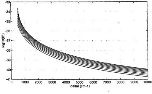
must also be increased. However, increasing c or X is undesirable. The object is to produce as short a pulse as possible, and it is difficult to fabricate a DFB with a very high coupling coefficient. Figures 4.2 and 4.3 graph second- andthird-order dispersion versus . Figure 4.4 graphs the ratio of eq (4.21) for
different pulsewidths.
Note that 8 can be a positive or negative quantity depending on which
side of the stop band is being used. One should also realize that the
propagation constant can be positive or negative and so can the group
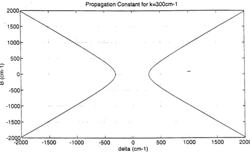
velocity and dispersion parameter. Since the mnodel is only concerned with forward waves, a positive group velocity is needed for whatever dispersion isnecessary. Figure 4.5 graphs the propagation constant versus and Table 4.1 below lists the sign of ,
3,
'=l/Vg, and " for each quadrant. Once thetheoretical analysis is completed, the dispersion needed will be known, and
Table 4.1 will be useful in figuring out the right parameters to use.Second-Order Dispersion for k=160 to 400
Ideltal (cm-1)
Figure 4.2. Second-order dispersion versus 11 for K=160 to 400cm-1.
m lo
Ideltal (cm-1)
)00
Ratio of Third- to Second-Order Dispersion for 5,10, and 15ps pulses
0 1000 2000 3000 4000 5000 6000 7000 8000 9000 10000 Ideltal (cm-1)
Figure 4.4. pulses.
Ratio of third- to second-order dispersion for 5, 10, and 15ps
Propagation Constant for k=300cm-1
co
-9nnn I I I
-2000 -1500 -1000 -500 0 500 1000 1500 2000
delta (cm-1)
Figure 4.5. Plot of both positive and negative propagation constants, A, versus
Table 4.1. Signs of propagation parameters in the four quadrants as referred to in Figure 4.5. I II
III
1
V
6-
+ + P +-'
+ + + p"-
. + +4.4 Matching Structure
In this ring model, the wave should propagate in only one direction. There will be reflections from the DFB traveling in the opposite direction and
because this model has an isolator on one side of the diode, the energy in
these waves will be lost. Furthermore, the reflected waves that travel
through the diode will deplete the carrier density of the diode and decrease
the gain. Therefore, it would be helpful to add a structure on each end of theDFB structure to match the grating to the diode- and thus decrease the
reflection coefficient seen by the wave when first entering the DFB structure.The reflection coefficient is r=A/B can be expressed as a function of position, z, in terms of the reflection coefficient at z=0, ro=r(z=0), using the coupling equations (4.10-11):
-jsinf z + F cospz + j sinfiz
cosfiz
- js
+ j sinz
jF
0sin
IC IC (4.22)
where [i is the propagation constant of the DFB as in eq (4.17).
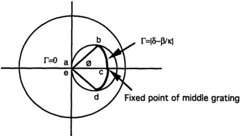
Figure 4.6 shows the entire structure where-the middle grating is for
chirp compensation and the grating and gaps on either side is for matching purposes. The initial assumption in the analysis of this structure is that the reflection coefficient at z=0 is zero. As shown by Haus [6], the reflection coefficient as a function of distance can be described by the Smith chart, Figure 4.7.
r=
e L ~ z=0
P/Kl
it of middle grating
Figure 4.7. Smith chart model following F of the matched DFB structure.
Beginning at z=0, the reflection coefficient is zero, represented by the origin of the chart (a). Traveling away from z=0 in the negative direction, the reflection coefficient follows a circle as shown in the figure until the end of the first section of grating(b). In the gap between the first and middle gratings, the reflection coefficient follows a circle concentric to the origin since the gap simply provides a phase shift dependent on its length. The length of the first grating and the gap should be such that the reflection coefficient at the end of the gap matches that of the middle grating when driven by its eigensolutions. This reflection coefficient from (4.10-11) is simply:
r=6-K (4.23)
When driven by the eigensolution, the reflection coefficient of the middle grating remains constant throughout the grating(c).
Another gap of the same length after the middle grating shifts the
coefficient again onto the circle of the first grating (d). Through the last section of grating the reflection coefficient follows that circle back to the origin as depicted in the figure (e). Thus, both ends of the structure have a reflection coefficient of zero.The length of the two end gratings and the gaps are determined by the magnitude of the reflection coefficient of the middle grating, In order for matching to occur, the magnitude of
r
at the end of the first grating (and at the beginning of the second grating) must be the same as the middle grating:r=-P
K (4.24)
Eq (4.12) can be simplified by setting rF=0, and the length of the end gratings can be found by setting eq (4.12) equal to eq (4.24):
= sin- C
k2 (4.25)
The length of the gap is determined by the phse shift required to transform r to the that of the middle grating:
(
= r
-tan-'
J
tan
Pt
2
f j(4.26)
and the length is:
coon (4.27)
co. and 60 above refer to the values of to and 6 at which a perfect match is
obtained.
The matching structure should be designed for the center frequency of the signal, i.e. the carrier frequency of the diode. The bandwidth of this structure will be analyzed once the parameters are set. Hopefully, F will be
less than .1 over the bandwidth of the pulse (but don't hold your breath).
4.5 Coupling Coefficient
The magnitude of the coupling between the forward and backward
wave is expressed by the coupling coefficient, K. Power conservation dictatesthat:
Kab = K, = jK (4.28)
The evaluation of Kc for a particular DFB structure is given by Haus [7].
.W
-
2iUOk
cos
2kd
'ab
=-Jk,
(e
- e)h
4
k,d + sin 2kd+-
cos kd
2 Cx (4.29)
K is shown to depend on the difference in dielectric constants between the
inside (ei) and the outside (e) of the waveguide, and also on the amplitude of the perturbations (h).
It can be seen from (4.29) that K increases with increasing perturbation amplitude and increasing difference in dielectric constants.
Unfortunately, it becomes increasingly difficult to fabricate a DFB with large perturbation amplitudes and dielectric differences, i.e. a high coupling coefficient. The highest coupling coefficient recorded to date is K=300cm-1, although generally K tends to be less than 200cm1.
Earlier a tradeoff was mentioned between pulsewidth and Kc in order to be able to neglect third-order dispersion. It would be nice if both could remain small, but rather than make the pulse too wide, K will be increased
beyond realistic bounds. However, very high coupling coefficients are
possible with photonic band gaps.Chapter 5
Simulation Models
5.1 Introduction
A printout of the program can be found in the appendix and has been
commented for easy reading. It was written in fortran simply because the
author of this thesis was most familiar with it. Most simulations were run
on the RLE VM systems.Following is a description of the algorithms used in simulating the
entire cavity. The program was developed in separate parts, the diode and the DFB structure, and later combined to form the entire ring.5.2 Simulating the Semiconductor Laser
The primary tools used for simulation of the semiconductor laser
diode were the rate equations given in section 3.3. (3.2) is used to determine the carrier density, and (3.3) is used to calculated the gain experienced by the field. The units of all the terms have not yet been discussed. P representsphotons per volume (eV/m
3), and field strength squared, or intensity, is
eV/s=Watts. The intensity, I a 12, and photon density are related by:
lal = vgAffP (5.1)
where Aeff is the effective transverse area of the active region. In order to
apply the rate equations, the present carrier and photon densities and current
value must be known. The photon density, P, on the right side of the rate
equations, is approximated as the incoming photons. The carrier density is given an initial value determined by the dc current, and is recalculated for every point in time using P and I, which is separately calculated for that time.The differential change in N is added to the current value to find N for the next point:
N2 = (go(N
V-
I- N,)la
/Ae'At+
N (5.2)where At is the time difference between points. In an effort to reduce error, the fourth-order Runge-Kutta method [8] was used to calculate the differential change in N.
The change in photon density is proportional to the difference between the intensity of the field going into the diode and the intensity of the field coming out, where intensity is the square of the field strength. Eq. (5.2) shows
that increasing intensity increases the photon density in the diode and thus
the intensity of the field exiting the diode. This is because more photonsentering the diode cause more stimulated emission and therefore more
photons to leave the diode. Finally the relation between the field strength and the differential change in photon density is:V dP = a 12 - ai12
dt a (5.3)
where a is the field coming out of the diode, ai is the field going in, and V is the volume of the diode. The intensity leaving the diode is:
la 12= (-xp + govgr(N - N,)P)Aeff + a, 12 (5.4) =
-gTp +
g
0(N
-
N,)e
+
l]ai2(5.5)
If (5.5) were to be expressed in exponential terms, it would be:
laol2 = a 12 exp( Vgp
+
ge(N - N,) (5.6)This shows that the simulation fits in very well with the mode-locking
theory.
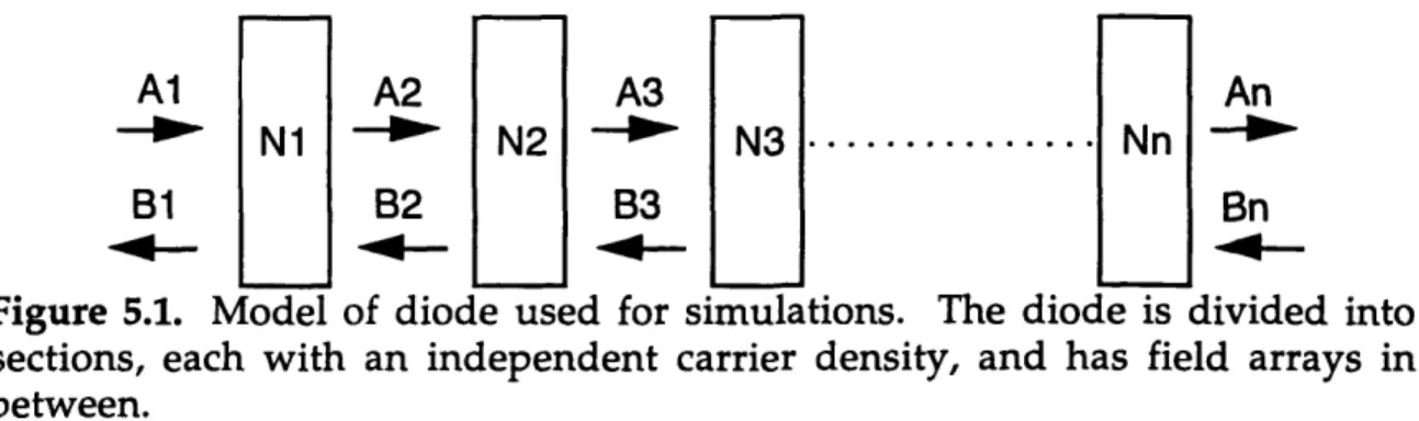
The above equations only work if the changes are very small, meaning that the diode is very short, especially because the shape of the pulse could change within the diode. The entire diode is too long, so it is divided up into sections. The carrier density is calculated separately for each section although
they all start with the same initial value.
So far, only the change in amplitude has been determined, but due to propagation through the diode and its nonlinear effects, the phase is greatly changed as well. Assuming that each section is short enough, propagation
Al A2 A3 An _- Ni -W N2 -N' N3.. ... Nn -- P
B1 B2 B3 Bn
Figure 5.1. Model of diode used for simulations. The diode is divided into
sections, each with an independent carrier density, and has field arrays in
between.
and nonlinearity is applied separately from the gain, thus at this point the
signal has the same phase as it did going into the diode. This intermediatepulse (old phase, new amplitude) is transformed, propagated and transformed
again. After propagation, the time dependent nonlinearity is applied, so it isimportant that the carrier density throughout the pulse is recorded.
The most difficult part of simulating the diode was to find a way to propagate both forward and backward waves through the diode. The solution was to take the forward and backward fields through each section of diode impulse by impulse. This means that the time it takes to travel through each section has to be the same as the time difference between impulses. Between each section, there is an array to which the output of the previous section is added. There are separate arrays for the forward and backward waves (Figure
5.1). The intensities of the forward and backward fields are added when
calculating the differential change in carrier density, but separate when
determining the gain for the two fields. This is correct because the stimulated emissions are emitted in the same direction as the original photon and there is no coupling. Propagation and gain are almost linear functions for a short diode which allows the effects to be additive, but the nonlinearity factor is not. The nonlinearity is applied separately to each impulse before it enters the next section, where the nonlinearity corresponds to the previous section. Thus the error in simulating the diode is minimized.The DFB structure is actually not expected to produce significant
reflections using the matching structure. However, if the bandwidth of the
pulse exceeds that of the matching structure or if the ring model is changed toa cavity model, then this program is prepared propagate both directions.
The final effect of the diode is the bandlimiting factor. To include this, the pulse was filtered outside of the diode. The filter is lorenzian, and the bandwidth is on the order of terrahertz.