Chemical and Biological Sensors Based on
Semiconductors
by
Mihail Bora
Submitted to the Department of Physics
Organic
MASSACHUSETTS INSTITUTE
OF TECHNOLOGY
AUG
0 4 2009
LIBRARIES
in partial fulfillment of the requirements for the degree of
Doctor of Philosophy in Physics
at the
MASSACHUSETTS INSTITUTE OF TECHNOLOGY
March 2009
@ Massachusetts Institute of Technology 2009. All rights reserved.
ARCHIVES
Author ...
Department of Physics
March 13, 2009
Certified by ...
Marc A. Baldo
Associate Professor
-
-esis
Supervisor
Certified by...
/. -. . . .Alexander van Oudenaarden
Professor
Thesis Supervisor
Accepted by ...
f
J
Thomas Greytak
Chemical and Biological Sensors Based on Organic
Semiconductors
by
Mihail Bora
Submitted to the Department of Physics
on March 13, 2009, in partial fulfillment of the
requirements for the degree of
Doctor of Philosophy in Physics
Abstract
In this thesis I designed, fabricated and characterized two types of sensors: chemical
sensors based on organic thin film transistors, and a miniaturized surface plasmon
resonance biosensors for biotechnology and medical diagnostics applications. During
completion of my research projects I designed and optimized several device
archi-tectures using numerical simulations and fundamental physical evaluation of sensing
mechanism and performance. Fabricated devices were tested in custom built
exper-imental setups in microfluidic testing chambers using automatic data measurement.
Surface functionalization of device surface using self assembled monolayer techniques
was employed for experiments that required specificity towards analyzed biological
species.
Thesis Supervisor: Marc A. Baldo
Title: Associate Professor
Thesis Supervisor: Alexander van Oudenaarden
Title: Professor
Acknowledgments
I am thankful to my research advisor, Professor Marc Baldo for financial and academic
support for a large portion of my doctorate. I would also like to thank my thesis
co-advisor in the Physics Department, Professor Alexander van Oudenaarden in whose
group I spend close to one year. The summer financial support and mentoring was
greatly appreciated. To the rest of my thesis committee, Professor Sebastian Seung
and Professor George Benedek, thank you for the time and comments related to my
research.
I greatly enjoyed working with my colleagues. I thank Tim Heidel, with whom I
worked on the organic semiconductor transistor sensors.
For the biosensor project, there are so many people I am indebted to: Kaveh
Milaninia, for help building the experimental setup and all the clean room
fabrica-tion, Kemal Celebi, who developed the simulation software for both detector and light
source, Jorge Zuniga, Colin Watson and Carlijn Mulder for their work on device
fabri-cation, Liselotte Kaiser and Ky Lowenhaupt for help with surface plasmon resonance
assays and instrumentation, Oktay Uzun for advice on self assembly and
function-alization methods, Yong-Ak Song that shared expertise, materials and facilities for
fabrication of microfluidic components.
I thank Priya Jadhav and Benjie Limketkai for insightful discussions on charge
transport in organics, related to measurement of density of states, percolation theory
and performance of the organic thin film transistor sensors.
I don't want to forget the rest of the group Jiye Lee, Mike Currie, Shlomi Goffri,
Michel Segal and my colleagues next door with whom I collaborated on the carbon
nanotube nano-fabrication project: Alfonso Reina, Hootan Farhat, Mario Hoffman,
for advice related to nanotube growth and characterization, and Kaveh, for his help
building the cold development experimental setup. I thank Luke Theogarajan for his
availability to always take a critical look at my ideas and hypotheses.
My work could not have been completed without financial support from DuPont
and the Institute for Soldier Nanotechnologies.
Finally, I thank my wife Emilia for her love, and the rest of my family for their support: Florin, lulia, lulian, Ilinca and my father, Patru. I dedicate this thesis to the memory of my mother, Maria.
Contents
1 Motivation
21
2 Review of surface plasmon resonance sensors and instrumentation 25
2.1 Introduction ... 25
2.2 Advances in surface plasmon resonance technology ... 30 2.2.1 Data analysis of surface plasmon resonance sensors . . . . .. 30 2.2.2 Signal referencing for improved SPR accuracy . ... 31 2.2.3 Surface plasmon resonance sensors based on phase detection 31 2.2.4 Surface plasmon resonsnce sensors for absorbing media . . .. 32 2.2.5 Integration of SPR sensors with Mach-Zehnder interferometer 32 2.2.6 Long-range surface plasmons for high-resolution surface
plas-mon resonance sensors ... ... 32 2.3 Optical fiber surface plasmon resonance sensors . ... . . 34 2.3.1 Spectral fiber optic sensor based on surface plasmon resonance 34 2.3.2 Control of the dynamic range and sensitivity of a surface
plas-mon resonance based fiber optic sensor . ... . . 34 2.3.3 Optical fiber affinity biosensor based on localized surface
plas-mon resonance ... ... 35
2.3.4 In-line fiber-optic sensors based on the excitation of surface plasma modes in metal-coated tapered fibers . ... 36 2.3.5 Fiber optic sensor based on gold island plasmon resonance . . 37 2.4 Surface plasmon resonance sensors based on diffraction gratings . . . 37 2.5 Localized SPR: surface plasmons on metal nanoparticles . ... 38
2.6 Integration of surface plasmon resonance instrumentation ... 2.6.1 Spreeta ...
2.6.2 Waveguide surface plasmon resonance sensors ...
3 Near field detector for integrated surface plasmon resonance biosen-sor applications
3.1 Abstract ... 3.2 Introduction ...
3.3 Results and Discussion ...
3.4 Sensor fabrication and experimental setup ... 3.5 Microfluidics ...
3.6 Binding kinetics of analytes ...
4 Integrated surface plasmon resonance biosensor based on organic semiconductor devices
4.1 Introduction ...
4.2 Results ... ...
4.3 Optimization of the near field plasmon detector .. . . . ...
4.4 Performace of the integrated OLED-near field plasmon resonance de-tector device . . . . ...
4.5 Discussion ...
5 Combinatorial detection of volatile organic compounds using
metal-phthalocyanine field effect transistors 5.1 Abstract ... 5.2 Introduction ...
5.3 Theory ... ...
5.3.1 Steady state analysis . ... ... 5.4 Experimental results ... 5.5 Conclusion . . . . ... 6 Conclusion 55 55 56 60 62 63 65 65 66 68 68 73 78 81
A Numerical simulations for calculating relectivity, photocurrent and
electric field amplitude in the plasmon detector
83
B Numerical simulations for calculating the angular emission from an
List of Figures
2-1 Plasmons are surface charge density waves propagating at a metal di-electric interface. ... . ... 26
2-2 Dispersion relation for surface plasmons (red), light in vacuum (black) and light in an optical medium of refractive index n. ... 27
2-3 Surface plasmon excitation in the Kretschmann geometry. Surface plasmons are excited at the interface between the metal and low re-fractive index medium (left). A sharp dip in reflectivity is observed for angles of resonant energy transfer from incoming light into plas-mon modes. The coordinate of the resonance depends strongly on the dielectric constant of the medium adjacent to the metal. Binding of
biological species on the surface of the metal shifts the resonance to-wards higher angles and a change in reflectivity AR is measured to monitor analyte absorbance ... .... 28
2-4 Reflectivity dependence of angle for a gold film of varying thickness. On the left, reflectivity curves of 30 nm (green) 50 nm (red), and 70 nm (blue) gold fim for a 670 nm incident light. On the right, a two dimensional plot for angular reflectivity for a gold film of variable thickness from 20 to 100 nm. ... .... 29
2-5 Dual SPR sensor with a tantalum oxide overlayer grown on top of the SPR active metal. ... . ... 31
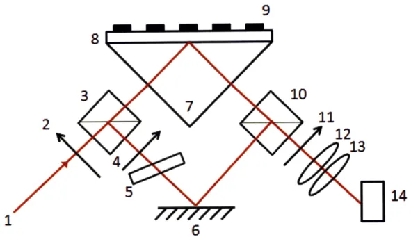
2-6 Experimental setup for integration of a Mach-Zehnder interferometer with a surface plasmon resonance sensor. Scheme of SPRI imaging: light beam (1), polarisers (2,4), beam-splitting cubes (3,10), phase-retarding glass plate (5), mirror (6), SPR prism (7), gold film (8), patterned coating (9), analyser (11), imaging lenses (12, 13), CCD
camera (14) ... ... ... 33
2-7 SPR sensor based on single mode polished fiber ... 35
2-8 SPR fiber optic sensor with an optional high refractive index overlayer. 35
2-9 Schematic of gold tapered optical fiber sensor with asymmetric and symmetric metal layer. ... ... 36
2-10 Excitation of surface plasmons on diffraction gratings. The momen-tum difference between the incident and diffracted wave is transferred to plasmon waves propagating at the metal dielectric interface. The reflected beam monitors the strength of the resonance. . ... 38
2-11 Schematic diagram of the integrated SPR sensor. . ... . . 39
2-12 A schematic of the miniature surface plasmon resonance transducer
3-1 (a) Device structure and experimental setup. The near-field surface plasmon detector consists of a thin layer of a semiconductor sandwiched between two thin gold electrodes. The top gold electrode is circular with a radius of 1 mm. The top gold electrode defines the area of the detector and acts as the analyte binding surface. Biological materials are supplied by an autosampler through a microfluidic circuit. A p-polarized beam from a 1 mW laser at A=670 nm is aligned with the detector. The incident angle of the beam is adjusted by rotating the hemi-cylindrical lens with the detector attached. The reflected light and device photocurrent are monitored as a function of the incident angle and binding events on the top gold surface. (b) Photograph of a device integrated with a PDMS microuidic chamber and connecting tubing. A US quarter is also shown to illustrate the scale of the detector. 46
3-2 Simulation of the sensitivity of a near field surface plasmon detector as a function of the refractive index of the semiconductor material. The sensitivity is estimated from the change in photocurrent following the simulated binding of a thin protein layer on top of the device. It is plotted as a function of incidence angle of the optical source for a 50-nm-thick semiconductor with extinction coeffcient k=0.2 sandwiched between two 20-nm-thick gold layers. Higher sensitivity is achieved for lower refractive index materials, making organics a suitable candidate for plasmon detector applications. The maximum absorption in the photovoltaic is 0.4, hence the relative change in absorbance is 30%
(b) Structure of the near field surface plasmon detector and simulated amplitude of the electric field for the transverse magnetic mode within the device. Surface plasmon excitations have the highest amplitude on the top surface of the cathode layer but they also extend into the organic layers of the photovoltaic. Energy from the plasmonic mode is channeled into formation of excitonic states that dissociate at the hole and electron transport layer interface. . ... 47
3-3 The angular dependence of the photocurrent from the device (red cir-cles) and reflectivity (blue circir-cles). The solid lines represent trans-fer matrix numerical simulation for photocurrent (red) and reflectivity (blue) using n and k data measured for the materials used in device fabrication. The discrepancy between simulation and the data is most likely due to surface roughness in the gold electrodes. . ... 48
3-4 Sensor exposure to two water pulses in HEPES buffer flow. Both re-flectivity and photocurrent are modulated when the bulk dielectric constant of the medium above the device is decreased. The sensor shows excellent reversibility and stability. . ... . 49
3-5 Sensor response to casein and neutravidin. Green arrow: exposure to casein to block non-specific binding sites, orange arrow: specific detection of neutravidin. Both species bind irreversibly to the surface. The data demonstrates that the photocurrent response of the near field surface plasmon detector is equivalent to the conventional measurement
of reflectivity. ... ... 50
4-1 Integrated surface plasmon resonance biosensor consists of a microcav-ity OLED with off normal angular emission intensmicrocav-ity profile, a high index substrate and a plasmon detector sensitive to binding events on the surface of the sensor ... . . . ... 56
4-2 a)Device structure of the resonant cavity angular emission OLED. The top contacts form two mirrors with reflectivity coefficients R= 1 for the bottom and R=0.5 for the top. The length of the cavity is adjusted by varying the p-type spacing layer of TPD doped with 2% F4TCNQ. b) Experimental measurement of the angular intensity profile of the light emission from a resonant cavity OLED. The length of the cavity is ad-justed such that the intensity of emitted light is maximum off normal. c) Numerical simulation of the OLED output light intensity calculated using directly measured n and k values for the organic materials in Fig. 4-2(a). The discrepancy between the angular coordinate of the maxima is attributed to measurement error of material properties (n, k). 57
4-3 a)Electric field profile throughout the plasmon detector structure. b) Reflectivity and photocurrent for the considered device. ... . 58
4-4 Optimization thickness of bottom Au cathode . The thickness of the top contact is kept constant at 20 nm. The maximum sensitivity is observed for 27.5 nm ... ... 61
4-5 a) In black: plasmon reflectivity curves for a gold layer of 50 nm (dot-ted line), near field plasmon detector with optimal thickness bottom contact for gold (27.5 nm, solid line) and silver (17.5 nm, dashed line). In red: photocurrent resonance curves. b) Corresponding sensitiv-ity curves for the three cases considered. The detector structure is CuPc(20 nm)/C60(20 nm)/BCP(8.5 nm) . ... ... 62
4-6 a) Reflectivity plots for 50nm gold film (green) (theory), 50 nm gold film (orange) (experiment), detector (20 nm Ag, 20 nm CuPc, 20 nm C60, 8.5 nm BCP, 20 nm Au) (experimental data, blue), integrated device (normalized OLED intensity and detector) (experimental data, red). b) Photocurent plots for detector (experimental data, blue), in-tegrated device (normalized OLED and detector, experimental data,
5-1 (a) Numerical simulations for the geometry optimization of copper thalocyanine when stacked in a thin film. (b) Simulations of cobalt ph-thalocyanine in the presence of the solvent molecule acetonitrile. The solvent intercalation breaks the stacking of neighboring MPC molecules and effectively breaks a percolation pathway between the MPC sites. (c) The structure of the field effect transistor-based sensors studied in this work. A 10-nm-thick layer of metal-phthalocyanine (see inset) was deposited on a p-boron doped silicon wafer with 100-nm-thick thermal oxide. Gold source and drain contacts are patterned on top of the
organic. ... ... ... 74
5-2 (a) Ids vs. V, for Vd, -5 and -20 V and (b) Id, vs. Vd characteris-tics taken at Vgs = 0, -5, -10, -15, -20, -25 V for a ZnPc transistor. Solid lines represent data taken in a nitrogen atmosphere, and dotted lines data taken in 500 ppm acetone in nitrogen. Exposure to solvent decreases the conductivity of the channel but does not significantly influence the threshold voltage. ... .. 75
5-3 (a) The transient responses of ZnPC-based sensors were obtained by modulating the solvent concentration. Here, in a representative test of the stability of ZnPC sensors, we show the channel current modu-lation in a ZnPC sensor is exposed to 500 ppm ethanol (V, = -20V, Vds = -20V). To minimize the charging of deep traps in the channel
the gate voltage was applied for 100 ms, the channel current measured, and then the gate returned to zero bias for 4.9 s to allow de-trapping. After about 30 min the drain current is observed to stabilize although a slow decrease in channel current remains. (b) The linearity of MPC sensors is tested by modulating the solvent concentration. A repre-sentative result is shown here for a ZnPC sensor exposed to varying concentrations of toluene. The current modulation is observed to vary approximately linearly at low solvent concentration. . ... 76
5-4 (a) The steady state current modulation data AIds/Ids and (b), the
ratio of transient rates koN/kOFF upon exposure to 100 ppm of the
specified solvents. Combinatorial analysis yields unique 'fingerprints'
for each solvent. Transistor bias conditions are Vd, = -20V, V,
=
-20V. 77
5-5 (a) The concentration dependence of the steady state current
modu-lation data AIds/Ids for strongly interacting solvent-MPC pairs. (b)
The concentration dependence of the normalized fraction of adsorbed
solvent for the same pairs as calculated from the transient data. In
both (a) and (b) the lines are fits to Eq. 5.14 with a
=
80 ppm and
normalization constant
+/-
20%. Solid symbols correspond to toluene
and empty symbols to acetonitrile. Circles are CoPC, squares ZnPC,
upward triangles NiPC and downward triangles are CuPC. Note that
the weaker interactions are not well described by the simple kinetic
model since the Langmuir isotherm requires koN/koFF > 1. Although
this conclusion is tempered by the lower signal to noise and more
un-stable steady state response in the weakly interacting combinations.
.
78
List of Tables
Chapter 1
Motivation
Science and technology has progressed to measuring the environment in ways that extend well beyond the five basic senses in accuracy, physical properties, and limit of detection. Scientific discovery itself relies intrinsically on development of new sens-ing methods and tools. Of particular importance are sensors that measure chemical and biological species. Based on their operation mechanism, output, and application requirements, some sensors return a positive or negative value when a particular prop-erty exceeds a threshold value (the most common example being a carbon monoxide detector for chemical, or an off the shelf pregnancy test for biological species). Other uses require improved accuracy in measurement, as is the case of medical diagnostic tests, when analyte concentrations that fall outside an interval are indicative of a health hazard. In general, sensing is integrated in a feedback mechanism that alter-nates between measuring a state and altering it by external means. Pharmaceutical therapeutics cannot be administered without diagnosis and close monitoring of the
effects. Sensor uses characterize not only presence but also complex interactions be-tween species (e.g. binding kinetics) or even resolve some aspects molecular structure
(e.g. antibody epitope mapping).
The research projects in this thesis cover chemical sensors based on thin film tran-sistors, and biological sensors based on miniaturization of surface plasmon resonance sensors. For the transducing element both used organic semiconductors, chemical compounds of carbon that exhibit electrical conductivity that lies between that of
metals and insulators. For the thin film transistor devices the conductivity of the organic layer is modulated by applying a gate voltage and the transistor character-istics show dependence on the molecular species present in the surrounding medium. The main advantage of the organic materials is that they are amenable to chemical modifications and one can envision design of materials that performed sensing tasks with improved selectivity and specificity. In addition, the large variety of organics provides a library compounds for device fabrication. The same principles are used in the most common chemical sensor found in the living world, the olfactory system. It exploits the large diversity of olfactory receptors, by far the largest family of re-ceptors in the mammalian genome. It is estimated that as much as 2% of the mouse genome encodes olfactory proteins. The olfactory system concept was adapted to an electrical system consisting of an array of transistors, also known as electronic nose. The response of the array to an analyte provides fingerprint response the same way the biological system relays a complex sensation from the nasal organ.
Chemical sensors based on organic this film transistors are primarily driven by low cost applications that do not demand stringent sensing requirements as is the case of food industry monitoring in which quality control assurance is critical for public health. A typical example is spoilage of fruits or milk in which the detection system cannot exceed a small fraction of the total cost of the product.
Current biosensing methods were developed decades ago, independently of ad-vances in the microelectronics field, and do not leverage on parallel fabrication, pre-cision and reliability characteristic to semiconductor devices. The miniaturization of the surface plasmon resonance sensors described in this work aims at using function-alized solid state devices to detect biomolecular species in solution. The detection standards, ELISA (Enzyme Linked ImmunoSorbent Assay) and PCR (Polymerase Chain Reaction) rely on chemical amplification of either enzymatically processing a substrate into a measurable product or copying DNA strands. The consequence is that detectable levels take a significant time to accumulate (on the order of 3-4 hours), hence real time detection is not possible. Semiconductor devices do not need chemical amplification (although they can be used in conjunction with it) and real time
de-tection can be achieved. Several device structures have been proposed for solid state devices for biological sensors: micro electro mechanical devices (MEMs), electrical devices (gated transistors, resistors), miniaturized fluorescence, and surface plasmon resonance assays[1]. While each method has its own drawbacks, the surface plasmon resonance seems to be the best candidate for successful replacement of current pro-teomic detection. MEMs used in aqueous environments (quartz crystal microbalance) suffer from significant dampening that decreases their sensitivity. A potential
solu-tion to this problem is a microfluidic channel embedded in a resonating cantilever. The sensitivity of microcantilevers increases with smaller device size, hence a need for more complex fabrication processes. Electrical devices have to resolve the fact that bio-molecular species have poor electrical properties and that typical biological buffers have high ionic strength that usually interact with the gating mechanisms. Optical detection (fluorescence and surface plasmon resonance) has the advantage of being most robust. Fluorescence detection requires labeling that increases the assay complexity and has the potential to disrupt the binding mechanism between molecu-lar species. Sensitivity is usually not sufficient for routine laboratory tasks and is most often used in microscopy studies. For the electrical and optical devices considered the sensitivity is independent of the device length scale, under the assumption of uniform distribution of analyte, hence the device size can be chosen more conveniently.
Surface plasmon resonance sensors exploit the sensitivity of surface plasmons to-wards changes in the dielectric constant of media at a noble metal -dielectric interface. The reflectance of a gold film directly measures surface binding of proteins have a higher refractive index then the buffer in which they are dissolved. The main chal-lenge for SPR is that changes in the refractive index are not always related to the binding assay. Of prime importance is precise control of temperature since the density (refractive index) of fluids depend linearly with temperature. The real time detection feature of SPR enables direct measurement of binding kinetics between the species immobilized on the surface and the one in solution. Surface plasmon resonance tech-nology has its commercial uses in the research and development of the pharmaceutical industry for drug development applications. It is estimated that bringing a single new
drug to market costs over $800 million and takes 10-15 years. Drug development starts with screening of huge compound libraries against bio-molecular targets responsible for diseases. The best candidates are selected based on the strength of interaction (binding) with the target that usually disrupts the disease progression pathway. The ability of SPR to measure directly the dissociation constant, the main indicative of binding strength, makes it the optimal technology for compound screening in drug de-velopment. In addition, the instrumentation can be easily automated for continuous operation.
The high price of SPR makes it suitable for applications in which high throughput is critical. Miniaturization of SPR aims at decreasing the cost of consumables and instrumentation so that the benefits of the technology can be introduced to users that do not support a high price point. Most obvious is the area of medical diagnostics that could benefit from a sensing method that is fast, economical, reliable and sensitive. The current diagnostics test, ELISA achieved a fairly low price point mainly due to processing in large batches at centralized locations, but suffers from slow detection speed. The present work on surface plasmons shows encouraging prospects towards making SPR a routinely used choice in a variety of research and industry settings.
Chapter 2
Review of surface plasmon
resonance sensors and
instrumentation
2.1
Introduction
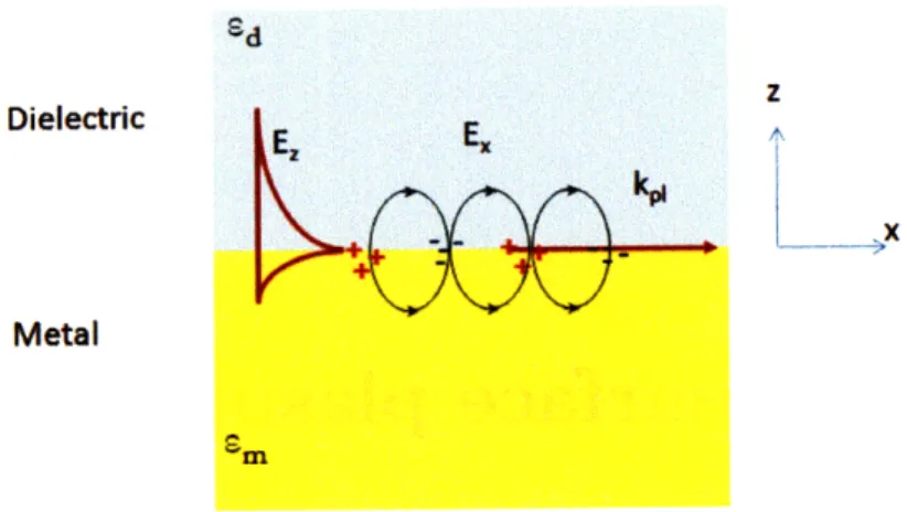
Surface plasmons are electromagnetic waves that propagate along a metal dielectric interface. They are solutions to Maxwell's equations for transverse magnetic (TM) modes. On both sides of the metal and dielectric the electric field decays exponentially with distance. A surface charge density propagates along the boundary between the two media with a wavevector given by:
G = i Eam (2.1)
c Ed±m (2.1)
where w is the angular frequency, c is the speed of light, Ed and ~m are the dielectric constants of the dielectric and metal. In order to have a positive wavevector kl the real part of the dielectric constant must be negative and its absolute value larger than the insulator dielectric constant. The condition is satisfied for most metals such as silver, gold, aluminum, copper, platinum. The existence of surface plasmons requires frequencies lower than a certain critical value, A that depends on the plasma
frequency.
Z
Dielectric EEx
Metal
Figure 2-1: Plasmons are surface charge density waves propagating at a metal dielec-tric interface.
Plasma oscillation of surface electrons are coupled to electromagnetic radiation in several geometries. The Kretschmann configuration excites plasmons within a thin metal film placed between two insulators with different dielectric constants. The Otto configuration excites plasmons through the evanescent field of a total inter-nally reflected beam. In this case a spacer layer between the coupling prism and metal film is present. Surface plasmons can also be excited on gratings when the horizontal momentum transferred by the diffracted light beam matches matches the momentum of plasmon waves. A particular case is plasmon coupling through surface roughness when the Fourier transform component of the wavevector matches peri-odicity conditions required by grating excitation. Metal nanoparticles also support surface plasmons excited by incident light, although it is important to notice that the plasmon dispersion relation is different from that of planar metal films.
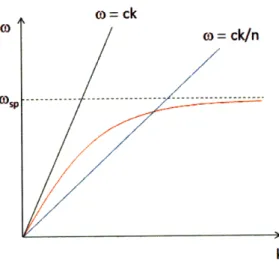
The Kretschmann configuration for excitation of surface plasmons can be under-stood from the dispersion relations of both plasmons and light. Fig. 2-2 shows the
w(k) dependence for surface plasmons, and light in vacuum and an optical medium.
The light propagating in vacuum and plasmon dispersion curves intersect only in ori-gin, meaning that there is no physical solution for coupling between the two states. On the other hand the light line for denser medium has a smaller slope and
inter-) = ck
O" /0 = ck/n
CD p . . . .. .- - - . . . .. . . . .--- --- ---- --- .-- - -- - --
-k
Figure 2-2: Dispersion relation for surface plasmons (red), light in vacuum (black) and light in an optical medium of refractive index n.
sects the plasmon curve in one additional point corresponding to surface plasmon resonance.
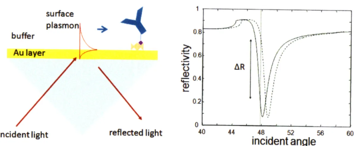
A typical experimental setup and results for plasmon excitation in the Kretschmann geometry is presented in Fig. 2-3. A laser beam falls on a gold film through an glass prism that has a refractive index higher than the immersion buffer. As the incidence angle is scanned, a resonant feature in the film reflectivity occurs when surface plas-mons are excited beyond the total internal reflection angle between the glass and the buffer. The resonance location depends on the electromagnetic properties of the prism, metal layer and buffer.
When bio molecular species are absorbed on the metal surface the small changes in the dielectric constant change the resonance coordinate, hence measuring the reflec-tivity at the highest slope provides a means of monitoring real time binding kinetics. The sensitivity of the techniques is higher with narrow resonances, hence less lossy metals are preferable. While silver has the lowest plasmon full width half maximum (FWHM), in practice gold is preferred because it does not form a native oxide layer under common measurement conditions. It is important to notice that the shape of the resonance is asymmetrical with the right side having a significantly lower slope. The reflectivity (or amplitude) measurement is therefore performed on the left arm
for a better signal to noise ratio. surface plasmon . buffer \-Au layer 06 o 0.4-0.2 0 i L . J ..
Incident light reflected light 40 44 48 52 56 60
incident angle
Figure 2-3: Surface plasmon excitation in the Kretschmann geometry. Surface plas-mons are excited at the interface between the metal and low refractive index medium (left). A sharp dip in reflectivity is observed for angles of resonant energy transfer from incoming light into plasmon modes. The coordinate of the resonance depends strongly on the dielectric constant of the medium adjacent to the metal. Binding of biological species on the surface of the metal shifts the resonance towards higher angles and a change in reflectivity AR is measured to monitor analyte absorbance
The angular reflectivity spectra exhibit dips that correspond wiht the transfer of energy from the incident light wave into a surface plasmon and later dissipated in the metal film as heat. A SPR curve with minimal reflectivity as well as steep slope is observed for an optimal thickness of approximately 50 nm (Fig. 2-4). For gold films with a thickness larger than the optimal value, an SPR curve with a broader width, a higher minimum, a greater resonance angle,and a less steep slope is observed. For gold films with thicknesses greater than the optimal value, an SPR curve with a slightly smaller resonance angle, and greater reflectivity minimum is observed. The width and the asymmetry of the reflectivity dip increase with the decreasing metal thickness.
The surface plasmon resonance technique offers great sensitivity for molecules with relative high molecular weight, complemented by real time detection and no need for labeling that might interfere with the analyte biochemical functionality. Table 2.1 shows a comparison between SPR and other routinely used sensing methods[l]. In addition to excellent sensitivity, surface plasmon resonance offers real time detection,
Reflectivity 0.5 Reflectivity S100 0.8 0.6 _____
60o
0.4 02 035 40 45 50 55 60 65 70 5 40 45 50 55 60 65 70incidence angle incidence angle
Figure 2-4: Reflectivity dependence of angle for a gold film of varying thickness. On the left, reflectivity curves of 30 nm (green) 50 nm (red), and 70 nm (blue) gold fim for a 670 nm incident light. On the right, a two dimensional plot for angular reflectivity for a gold film of variable thickness from 20 to 100 nm.
Table 2.1: Detection limits of protein and cellular sensing techniques.
Measurement technique
Platform
Target
Sensitivity
Surface Plasmon Resonance
Refractive index Protein, Cell 10 pg/mm
Enzyme Linked ImmunoSorbent Assay Absorbance
Protein
10 pM
Quartz Crystal Microbalance Mass Protein, Cell 1 ng/mm'
Microcantilever Mass Protein, Cell 0.5 ng/mm'
Polymerase Chain Reaction RNA copies mRNA 100 pg/ml
Immuno-Assay MultiPhoton Detection Radioactivity Protein 10 fg/ml
direct measurement of binding kinetics, integration with microfluidics for decreased sample size and increased throughput. The SPR assays do not use any labeling that might interfere with the biodetection mechanism.
In the past decade, surface plasmon resonance commercial instrumentation has been widely available from a variety of manufacturers (Biacore, GWC Technologies, Reichart Life Sciences, Bio-Rad Laboratores, ICx Nomadics), due to the fast adoption the technology.
2.2
Advances in surface plasmon resonance
tech-nology
2.2.1
Data analysis of surface plasmon resonance sensors
The reliability of surface plasmon resonance data depends on the accuracy of collecting data. Averaging n data points results in a decrease by a factor of nl/2 in the noisestandard deviation. One of the methods of finding the resonance minimum, called the centroid method, calculates the geometric center of the resonance minimum for data points above a certain threshold. Usually it does not coincide with the local minimum because the plasmon dip is asymmetrical. The final measurements are not affected since SPR experiments monitor relative shifts. When the light source intensity output fluctuates the spectrum is raised or lowered relative to the threshold value and the method leads to erroneous results due to resonance asymmetry. This shortcoming is solved by using an interpolating centroid tracking method. First, the data is interpolated so that the endpoints of the angular (wavelength) interval are assigned only a partial weight. Then the tracking interval is set to be roughly the full width at half minimum (FWHM). After the resonance shift the algorithm flollows
the data curve and positions the tracking span such that the endpoints have equal
value[52].
There are a variety of sources that change the output of an SPR sensor: ana-lyte binding on the gold surface, temperature changes, mechanical instabilities, noise caused by the light source, detector or electronics. Usually, the largest contribution of noise comes from the photo-detector. It can be subdivided in several categories: shot noise (light intensity dependent) corresponding to fluctuations in the incoming light flux and carrier generation in the photo-detector, thermal noise, dark current noise, and readout noise of electronic interface. Typical charge coupled device (CCD) detectors achieve a resolution of 2 * 10-7 RIU (refractive index unit), and substitution with photo diode array (PDA) detectors achieve even higher detection limit of 2 * 10- 8 RIU. The main challenges of low noise measurements are increasing the intensity of
the light source and the throughput as typical SPR data points are collected every 1-5 s.
2.2.2
Signal referencing for improved SPR accuracy
A better signal to noise ratio and consequently improved stability and detection limit
is achieved with parallel sensing channel architecture[31]. The incident light beam falls on a region divided in an active sensing layer and bulk background monitoring layer. The method allows for discrimination between bulk and surface effects and identify sample refractive index variations and non specific molecular binding.
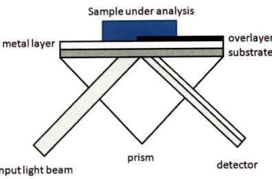
Sample under analysis
metal layer
overlayer
substrate
pnsm
input light beam
detector
Figure 2-5: Dual SPR sensor with a tantalum oxide overlayer grown on top of the SPR active metal.
2.2.3
Surface plasmon resonance sensors based on phase
de-tection
Most common SPR measurements are performed in the Kretschmann configuration at fixed angle of incidence and fixed wavelength and measure metal film reflectivity (amplitude). The Fresnel surface plasmon resonance model also predicts a rapid change in phase of the TM reflection that has a steep slope over a small range of refractive indices of the medium in the vicinity of the silver film[51, 60]. The sensitivity is comparable to that of amplitude SPR sensors in the range of 5 * 10- 7 RIU. The
theoretical model predicts that the phase change and sensor's dynamic range has a
strong dependence on the thickness of the metal layer.
2.2.4
Surface plasmon resonsnce sensors for absorbing media
Surface plasmon excitation in the ATR (attenuated total reflection) configuration can
be used to increase the absorbance of the sampled medium that can be explained due
to an increased interaction length of plasmons along the metal plane[36]. As expected
the optimal sensitivity silver thickness in the case of absorbing medium (48 nm) is
lower than the one optimized for non-absorbing dielectrics (55.5 nm) for the 670 nm
wavelength considered.
2.2.5
Integration of SPR sensors with Mach-Zehnder
inter-ferometer
Nikitin et. al. integrated a prism coupled surface plasmon resonance sensor into one
arm of a Mach-Zehnder interferometer[55] Figure 1. An enhanced sensitivity is
at-tributed to phase change shift and interferometric imaging provides spatial resolution
on the micron scale that opens up possibilities for microarray imaging[73, 35]. A
mixture of 0.001% of glycerol in water resolved a resolution of 10-7 RIU, attributed
to the faster response of the phase to changes in the refractive index then that of the
reflected intensity.
2.2.6
Long-range surface plasmons for high-resolution
sur-face plasmon resonance sensors
Improvements in SPR sensitivity can be achieved by using long range surface plasmons
(LSPR) [53]. The method uses thinner metallic films (20-40 nm) that are sandwiched
between symmetric dielectric mediums. Since in the case of biological sensors one of
the sides of the metal layer is exposed to aqueous solutions, a low refractive index
buffer made of Teflon (n=1.31) or magnesium fluoride (n=1.38) is intercalated
be-1
177
6
Figure 2-6: Experimental setup for integration of a Mach-Zehnder interferometer with a surface plasmon resonance sensor. Scheme of SPRI imaging: light beam (1), polarisers (2,4), beam-splitting cubes (3,10), phase-retarding glass plate (5), mirror (6), SPR prism (7), gold film (8), patterned coating (9), analyser (11), imaging lenses (12, 13), CCD camera (14).
tween the coupling prism and metal film. As the metal film decreases in thickness bellow 50 nm, surface plasmons will be excited on both surfaces of the film. Their interaction can be either symmetric (low losses, long propagation length) or anti-symmetric (high losses, short propagation length). The longer propagation length, or long range surface plasmons have a more narrow width and higher sensitivity then the conventional SPR.
Excitation of long range surface plasmons require dielectric media with similar re-fractive indices on both sides of a noble metal[71]. The dielectric buffer layer between the high index prism and metal film, Cytop (a fluoro polymer) can be spin coated to an 1180 nm thickness. A significant decrease in the resonance full width half max-imum height is observed in the case of LSPR (FWHM=0.15 degrees) compared to conventional SPR (FWHM= 1.2 degrees). Since the low thickness of dielectric buffer layer exceeds the light wavelength (814 nm), the plasmons are excited by the
evanes-cent field of a total internal reflected light beam, the so called Otto configuration. The sharper profile of the long range plasmon resonance enables better sensitivity compared to the standard SPR approach. One of the drawbacks resides in the fact that long range plasmon penetration depth in the sampled medium (buffer) is larger than the conventional case of 200 nm. The LRSPR is used for imaging of DNA hy-bridization of microarrays chips and a detection limit of 5 nM is resolved for binding of a 16-mer single stranded DNA sample.
2.3
Optical fiber surface plasmon resonance
sen-sors
2.3.1
Spectral fiber optic sensor based on surface plasmon
resonance
A surface plasmon resonance miniaturized sensor is based on a fiber optic sensing element[62, 61, 30, 25]. The side of the fiber is polished to the core and a layer of gold of variable thickness (45-75 nm) is evaporated. The fiber transmission is measured over a spectral range of 750-950 nm and a minimum is observed for wavelengths that are coupled most efficiently into plasmon modes in the gold film. Upon changing the refractive index in which the sensor is immersed a shift in transmission minima of the optical fiber occurs. Further, it is shown that the shift depends linearly on the refractive index of the sampled fluid with a limit of detection of 5*10-7. A specific biochemical assay between human immunoglobulin (IgG) and monoclonal antibody
against (IgG) measured shifts of up to 5nm.
2.3.2
Control of the dynamic range and sensitivity of a
sur-face plasmon resonance based fiber optic sensor
In a variant of surface plasmon resonance sensors based on silica core optical fibers, gold is deposited at the tip around the stripped core[34]. A highly reflective silver
sample
over-layer
cladding
metal
film
Ncore
single mode optical fiber
Figure 2-7: SPR sensor based on single mode polished fiber.
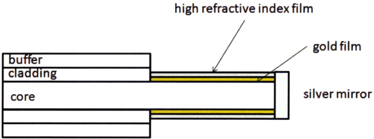
mirror is deposited on the flat polished end for signal enhancement. response of fiber transmission provides medium limit of detection with a dynamic range between 1.25 and 1.40. The dynamic range 1-1.33 with the addition of a high refractive index layer (zirconium on the gold surface. A high refractive index core made of sapphire the dynamic range towards higher valued (1.45-1.72).
The wavelength of 5 * 10- 5 RIU can be tuned to oxide) deposited (n=1.77) shifted
high refractive index film
buffer
I
goldfilm
rlrdding
silver mirror
Figure 2-8: SPR fiber optic sensor with an optional high refractive index overlayer.
2.3.3
Optical fiber affinity biosensor based on localized
sur-face plasmon resonance
Mitsui et al developed an optical fiber that uses gold nanoparticles immobilized on the flat polished tip of the fiber[48]. The instrument can measure the spectral response
Il a II re I
w
| .. . . . I- . .. . . !
core
upon binding or monitor the back reflected light intensity in the fiber for a single wavelength excitation. In the amplitude measurement mode, the sensor shows great stability and a linear dependence between return light intensity and refractive index of the ambient medium. The device is tested to monitor binding kinetics of avidin on a biotin functionalized nanoparticle surface.
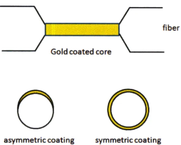
2.3.4
In-line fiber-optic sensors based on the excitation of
surface plasma modes in metal-coated tapered fibers
A version of optical fiber surface plasmon resonance sensor uses a gold coated tapered fiber as an alternative to side or flat and polished fibers[24]. Symmetric or asymmet-ric metal coating devices can be used either wavelength or amplitude output sensors. The symmetric configuration excites plasmons with azimuthal order m=l1, and are polarization insensitive, simplifying the sensor configuration and readout interpreta-tion. The log of optical fiber transmission depends linearly on the refractive index of the immersion fluid.
asymmetric coating symmetric coating
0
Figure 2-9: Schematic of gold tapered optical fiber sensor with asymmetric and sym-metric metal layer.
2.3.5
Fiber optic sensor based on gold island plasmon
reso-nance
A fiber optic based on gold island surface plasmon resonance is fabricated by stripping
the cladding from a doped silica fiber, evaporating a thin layer of gold and annealing the device for 4 minutes at 800 degrees Celsius[46]. Annealing tends to shape the islands into spheres and shift the plasmon resonance towards lower wavelengths. The limit of detection is fairly low, 0.1 RIU, but the dynamic range is greatly improved.
2.4
Surface plasmon resonance sensors based on
diffraction gratings
In addition to the attenuated total reflection geometry plasmons can be excited on diffraction gratings. After incidence on the grating the light is split into a reflected and diffracted beam of order m. A surface plasmon resonance phenomena occurs when the horizontal wavevector difference between incident and diffracted light matches the wavevector of the plasmon waves at the metal dielectric interface[26]. The light
plasmon coupling efficiency increases with the amplitude of surface height modula-tion and decreases for higher diffracmodula-tion orders. When the dielectric constant of the refractive index in the vicinity of the metal is changed, two symmetric plasmon dips are observed in the angular reflectivity of the film corresponding to diffraction orders m=1 and m=-1. Fabrication of diffraction gratings is based on photoresist exposure on a Mach-Zehnder interference pattern. After developer treatment the sinusoidal surface pattern is transferred onto a PDMS mold that was subsequently imprinted on a freshly spun UV curable polymer. After surface exposure to ultraviolet light the PDMS mold was peeled away a 50 nm layer of gold was evaporated. The sensor response measured as angle of resonance on a CCD detector array reach sensitivities of 5 * 10-6 RIU. Using multichannel multiplexed version of grating sensor device
fab-ricated on inexpensive plastic substrates, an array capable of monitoring thousands of sensing spots was demonstrated[26].
Reflected
light
Incident light
Diffraction order
m=-1
Surface plasmon
. I JbL~r
vV V
-
I
metallicgrating
Figure 2-10: Excitation of surface plasmons on diffraction gratings. The momen-tum difference between the incident and diffracted wave is transferred to plasmon waves propagating at the metal dielectric interface. The reflected beam monitors the strength of the resonance.
2.5
Localized SPR: surface plasmons on metal
nanopar-ticles
Siver nanoparticles were illuminated by a dark filed condenser and the light scattered by nanoparticles was collected by a microscope objective. The inverted microscope was equipped with an inverted spectrograph for recording the resonant Raleigh scat-tering spectrum of the nanoparticles[44]. The work demonstrates measurement of localized surface plasmon resonance (LSPR) on single silver nanoparticles that corre-lates into a zepto-molar range limit of detection. The system was used to measure the binding kinetics of 1-octanethiol self assembled monolayers and show a linear depen-dence between the Raleigh shift and the molecular weight of the species assembled on the surface.
In an article by Mock et. al.[50] silver nanoparticles were prepared by nucleating silver salts on 5 nm gold centers to an average diameter of 70 nm. The scattered light intensity profile is measured after immersion in oil with refractive indices from 1.44 to 1.56 and a linear dependence between LSPR shift and the index of the surrounding medium is observed. The sensitivity of the nanoparticles is dependent on their shape and plasmon resonance mode.
2.6
Integration of surface plasmon resonance
in-strumentation
A simple and compact realization of a SPR transducer was realized by using a laser
diode that provides and angular spread and a linear photodetector array that captures
reflectivity data for an interval of incident angles eliminating the need for mechanical
rotational stages[43]. The sensor is used to detect concentrations of water in ethanol
in the range of 0.3-10% and the temperature dependence of the signal from 20 to 25
oC was studied. Temperature compensated measurements with a reference channel
provided analyte concentrations with increased accuracy over a range of working
temperatures.
Flow chamber metal layer lens lens polarizer Photodiodearray LED prism (1024 ch.)Figure 2-11: Schematic diagram of the integrated SPR sensor.
2.6.1
Spreeta
One of the most successful approaches to integration of surface plasmon resonance
instrumentation was TI-SPR-1, co-developed between Texas Instruments and
Univer-sity of Washington[45]. The approach was to die mount and wirebond all electronic
components: an AlGaAs narrow band LED and a diode array detector. After
emis-sion by the LED the light passes an aperture (to limit the angular spread that enters
the system) and a polarizer (to limit introduction of TE modes that do not
con-tribute to plasmon excitations). The light is incident on a surface plasmon layer (50
nm gold) and is reflected by a reflective mirror coating on a linear silicon
photodi-ode array. An additional temperature sensor is included as refractive index of water changes approximately 10-4/loC. The geometrical relationships between components is fixed providing mechanical robustness and no need for alignment and maintenance during use. The integration and miniaturization incorporates simplified optics for high volume manufacturability and low cost.
Reflective mirror
Gold layer ,
'-4
Plastic prism
LED Photodiodearray
Figure 2-12: A schematic of the miniature surface plasmon resonance transducer TI-SPR-1.
The performance of Spreeta 2000 is discussed in terms of noise optimization tech-niques, accuracy and smoothness of the sensor[22]. For noise optimization the au-thors consider averaging and sum normalization and a detection limit of 1.8*10-7 is observed. The accuracy of the sensor is 0.2% over a change in RI of 0.04. The capabilities of the device are demonstrated by a binging assay for mouse IgG.
2.6.2
Waveguide surface plasmon resonance sensors
Harris and Wilkinson detail a theoretical evaluation of planar surface plasmon reso-nance waveguides[29]. The sensor measures optical transmittance through a rectan-gular optical waveguide whose evanescent field is coupled to surface plasmon modes on a planar metal film deposited across the waveguide. The transmission measured as the ratio between the outcoupled and incident power shows a sharp plasmon dip when plotted against the refractive index of the superstrate. The logarithm of transmis-sion, log(Pot) was measured for a series of waveguides varying in plasmon waveguide length from 1.5 to 5.4 mm in steps of 0.1 mm and a linear dependence with the gold film length was observed. The sensor environment was changed from 1 (air) to 1.330
(water) to study the sensitivity of the sensor towards changes in refractive index of the superstrate. A more complex sensor design that uses a dielectric low refractive index buffer layer between the optical waveguide and the metal film offered greater sensitivity.
A sensor design optimized for use in an aqueous environment is presented by Harris et al[28]. An optical waveguide is coated with a thin metal film that supports surface plasmons interacting within the sensing region. The optical mode passed through a 3dB splitter. After propagating through either the sensing or the reference arm the modes exit through the signal or reference waveguide. The sensor is used to measure concentration of simazine over a 10-100 ng/ml range using an antibody assay. Limit of detection is measured as 1 * 10-4 RIU.
Chapter 3
Near field detector for integrated
surface plasmon resonance
biosensor applications
3.1
Abstract
Integrated surface plasmon resonance biosensors promise to enable compact and portable biosensing at high sensitivities. To replace the far field detector tradition-ally used to detect surface plasmons we integrate a near field detector below a func-tionalized gold film. The evanescent field of a surface plasmon at the aqueous-gold interface is converted into photocurrent by a thin film organic heterojunction diode. We demonstrate that use of the near field detector is equivalent to the traditional far field measurement of reflectivity. The sensor is stable and reversible in an aqueous environment for periods of 6 hrs. For specific binding of neutravidin, the sensitivity is three times lower than a comparable conventional SPR biosensor. The sensitivity of the near field detector can be further improved by reducing surface roughness of the gold layers and optimization of the device design.
3.2
Introduction
Despite widespread demand there remains an unmet need for cost effective biosen-sors. Applications in research laboratories, home and point of care diagnostics, pro-cess industries, environmental monitoring, security and bio-defense, require the mea-surement of bio-analytes with high specificity and minimal time lag between sample collection and measurement readout. Among commonly used sensing methods, sur-face plasmon resonance (SPR) achieves relatively high sensitivity (0.5 ng/cm2) [1], and provides the benefits of label free detection and real time measurement of bind-ing kinetics, while integration with microfluidics reduces the sample size and enables high throughput [2]. SPR biosensors are highly versatile tools, being routinely used to examine protein - protein, antibody - antigen, and receptor - ligand interactions [3]. However, they are also large, difficult to transport and relatively costly, due to their dependence on precise calibration and alignment of the internal optics.
The disadvantages of SPR biosensors could be overcome by integrating the devices in solid state. As in other optical applications such as lasers, solid state integration can significantly reduce the footprint of the device, and improve the environmental stability in the presence of vibrations and temperature changes. The resulting de-vice contains three components: an optical pump, a near field detector for surface plasmons, and an aqueous interface with the bio-analytes.
In this work, we demonstrate integration of a near field surface plasmon detector [4] and the biorecognition interface of a traditional SPR sensor. The near field detector is used to replace the conventional far field optical detector. It is integrated directly with an Au/water interface that supports surface plasmons and acts as the binding site for bio-analytes. The integration of the optical detector is arguably the key challenge confronting the integration of a SPR biosensor. The remaining optical element, the optical pump, can be replaced by a microcavity light emitting diode (LED) [5, 6], or vertical cavity surface emitting laser (VCSEL) [7], placed under the near field detector and tuned for the wavevector of the plasmon resonance. Integration with an LED or VCSEL is not performed here, instead the integrated detector is characterized using
an external laser.
3.3
Results and Discussion
Conventional SPR sensors consist of a gold film deposited on glass and immersed in water [2]. The system is optically excited through the glass by a pump laser. When the angle of the laser beam incident on the Au/water interface hits the resonance, surface plasmons are generated at the Au/water interface and the reflected light drops markedly. The resonant angle is a sensitive function of the refractive index of all media within the range of the surface plasmon - typically -50 nm in Au and -200 nm in water. Thus, analyte binding events at the Au/water interface modify the coupling of light into the surface plasmon and are detected from variations in the optical reflectivity.
We seek to replace the far field measurement of reflected light with a direct near field measurement of the surface plasmons themselves [4]. The sensitivity of con-ventional SPR sensors is maximized for an approximately 50-nm-thick layer of Au deposited on glass [8]. But the electromagnetic field is negligible at the bottom of the 50-nm-thick Au layer, preventing near field detection of the surface plasmons below the Au. Thus, to efficiently detect surface plasmons at the aqueous interface with minimal change in sensitivity, we split the gold layer and insert a semiconductor; see Fig. 3-1.
To determine the ideal properties of the semiconductor, we calculate the sensitivity of a model near field SPR detector. The top and bottom gold layers are 20-nm-thick. The top surface of the device is immersed in buffer with a refractive index n=1.38. The substrate is glass with a refractive index n=1.72. The Poynting vector within the model device is calculated using a transfer matrix method assuming plane wave incident light [5]. To detect the surface plasmon in the near field the semiconductor must exhibit strong optical absorption. We assume that the semiconductor is 50-nm-thick with an extinction coefficient k=0.2. The sensitivity of the detector is calculated from the relative change in absorption within the semiconductor given the
(a)
Au cathode' u anode Glass substrate SPDOMS microfluidics Autosampler incident Agilent 1100 a eincident light reflected light
hemicylindrical prism n = 1.72
Figure 3-1: (a) Device structure and experimental setup. The near-field surface plasmon detector consists of a thin layer of a semiconductor sandwiched between two thin gold electrodes. The top gold electrode is circular with a radius of 1 mm. The top gold electrode defines the area of the detector and acts as the analyte binding surface. Biological materials are supplied by an autosampler through a microfluidic circuit.
A p-polarized beam from a 1 mW laser at A=670 nm is aligned with the detector.
The incident angle of the beam is adjusted by rotating the hemi-cylindrical lens with the detector attached. The reflected light and device photocurrent are monitored as a function of the incident angle and binding events on the top gold surface. (b) Photograph of a device integrated with a PDMS microuidic chamber and connecting tubing. A US quarter is also shown to illustrate the scale of the detector.
introduction of an interfacial 5-nm-thick protein layer with refractive index n=1.40. As shown in Fig. 3-2, we find that the sensitivity of the model device is maximized for semiconductor refractive indices between n=1.3 and n=1.8. The relative change in absorption within the semiconductor is 30% for the optimal choice of refractive index. When combined with the requirement for strong optical absorption, this calculation supports the choice of organic semiconductors for this application. For example, the archetype organic photovoltaic material copper phthalocyanine (CuPC) exhibits n=1.7 and k=0.2 at A=650 nm.
To compare the sensitivity of the near field detector to that of a conventional SPR, we also calculated the relative change in reflection from a 50-nm-thick Au layer. The same 5-nm-thick protein later with refractive index n=1.40 causes a 60% change in reflection, suggesting that the near field detector should exhibit roughly
(a)
(b)
water n=1.33 x 2.5 ) Au 20 nm "uc 55 60 65 70 75 80 45 50 55 60 65 70Incident angle (0)
Incident angle (0)
Figure 3-2: Simulation of the sensitivity of a near field surface plasmon detector as
a function of the refractive index of the semiconductor material. The sensitivity is
estimated from the change in photocurrent following the simulated binding of a thin
protein layer on top of the device. It is plotted as a function of incidence angle of
the optical source for a 50-nm-thick semiconductor with extinction coeffcient k=0.2
sandwiched between two 20-nm-thick gold layers. Higher sensitivity is achieved for
lower refractive index materials, making organics a suitable candidate for plasmon
detector applications. The maximum absorption in the photovoltaic is 0.4, hence the
relative change in absorbance is 30% (b) Structure of the near field surface plasmon
detector and simulated amplitude of the electric field for the transverse magnetic
mode within the device. Surface plasmon excitations have the highest amplitude on
the top surface of the cathode layer but they also extend into the organic layers of
the photovoltaic. Energy from the plasmonic mode is channeled into formation of
excitonic states that dissociate at the hole and electron transport layer interface.
half the sensitivity of a conventional device. The calculated sensitivity of the near
field detector should not be considered as a limit, however, since its structure contains opportunities for design optimization. For example, the bottom Au contact can be replaced by a lower loss Ag electrode.Consistent with the refractive index guidelines of Fig. 3-2, we design a practical organic semiconductor-based photovoltaic detector. The anode is a 20-nm-thick gold layer. The donor material within the organic photovoltaic is a 10-nm-thick film of CuPC. The acceptor material is a 10-nm-thick film of buckminsterfullerene (C60).
To increase optical absorption, a 20-nm-thick bulk heterostructure consisting of a
0 0.2 0.4 0.6 0.8 1 1.2 1.4 1.6 1.8