Advanced Modeling of Planarization Processes for
Integrated Circuit Fabrication
by
Wei Fan
B.S., Peking University (2004) M.S., Peking University (2007)
Submitted to the Department of Electrical Engineering and Computer in partial fulfillment of the requirements for the degree of
Doctor of Philosophy
in Electrical Engineering and Computer Science
at the
Massachusetts Institute of Technology
Science
A' VES
-S
September 2012
C 2012 Massachusetts Institute of Technology. All rights reserved.
Signature of A uthor: ... ... Department of Electrical Engineering and Computer Science
Advanced Modeling of Planarization Processes for
Integrated Circuit Fabrication
by
Wei Fan
Submitted to the Department of Electrical Engineering and Computer Science on August 6, 2012 in partial fulfillment of the requirements for the degree of
Doctor of Philosophy in Electrical Engineering and Computer Science
Abstract
Planarization processes are a key enabling technology for continued performance and density improvements in integrated circuits (ICs). Dielectric material planarization is widely used in front-end-of-line (FEOL) processing for device isolation and in back-end-of-line (BEOL) processing for interconnection. This thesis studies the physical mechanisms and variations in the planarization using chemical mechanical polishing (CMP). The major achievement and contribution of this work is a systematic methodology to physically model and characterize the non-uniformities in the CMP process.
To characterize polishing mechanisms at different length scales, physical CMP models are developed in three levels: wafer-level, die-level and particle-level. The wafer-level model investigates the CMP tool effects on wafer-level pressure non-uniformity. The die-level model is developed to study chip-scale non-uniformity induced by layout pattern density dependence and CMP pad properties. The particle-level model focuses on the contact mechanism between pad asperities and the wafer. Two model integration approaches are proposed to connect wafer-level and particle-level models to the die-level model, so that CMP system impacts on die-level uniformity and feature size dependence are considered. The models are applied to characterize and simulate CMP processes by fitting polishing experiment data and extracting physical model parameters.
A series of physical measurement approaches are developed to characterize CMP pad properties and verify physical model assumptions. Pad asperity modulus and characteristic
asperity height are measured by nanoindentation and microprofilometry, respectively. Pad aging effect is investigated by comparing physical measurement results at different pad usage stages. Results show that in-situ conditioning keeps pad surface properties consistent to perform
Acknowledgements
It has been five years since I first stepped on MIT campus. I cherish every day I experienced throughout my study at MIT. This work has been supported and guided by many people. I am truly grateful to all of them.
First, I must thank my advisor, Prof. Duane Boning, who has not only provided research support and guidance, but also advice and encouragement on my life and career. I have learned a lot of communication and collaboration skills from him. His passionate personality will inspire me throughout my life.
I would like to thank my thesis committee members, Prof. Jung-Hoon Chun and Prof. Judy Hoyt, for arranging meetings, and for their timely suggestions and feedback on my work.
This thesis consists of significant collaborations from both industry and academia. I am grateful to all my collaborators. Leslie Chains at JSR Micro in USA arranged the polishing experiments and provided the data for model fitting. Dr. Mansour Moinpour of Intel Corporation provided pad materials for my research. Dr. Yun Zhuang and Dr. Yasa Sampumo at the University of Arizona performed the pad aging experiment and prepared the pad samples for physical characterization. I would like to thank Prof. Ara Philipossian for many discussions on CMP, and it has been a great experience to collaborate with his group on CMP pad property study. I would also like to thank Dr. Len Borucki at Araca for sharing his experience and thoughts in CMP research.
My research has been constantly aided by the NanoLab and the Center for Materials Science and Engineering (CMSE) at MIT. I would like to thank Alan Schwartzman in the
subgroup meeting in the past five years. I would also like to thank Li Yu, John Lee and Albert Chang for sharing many interesting conversations about life.
In addition, I would like to thank Debb Hodges-Pabon, Mira Whiting and Grace Lindsay for their dedicated assistance.
A special thanks to my wife, Ying Wang, who has made my time in Boston so wonderful. Her love is always the best encouragement for my everyday life.
Finally I thank my parents for their support. I cherish every moment talking with them over the telephone and the internet. As their only child, I owe too much.
This work has been funded by SRC/SEMATECH Engineering Research Center for Environmentally Benign Semiconductor Manufacturing.
Contents
1
Introduction... 231.1g ... . 2 3 1.1.1 CMP in inter-level dielectric planarization...24
1.1.2 CMP in shallow trench isolation (STI) ... 25
1.1.3 CMP in damascene process for multilevel copper interconnection...26
1.1.4 Other applications of CMP ... 27
1.2 C M P process ... 28
1.2.1 C M P tool... . . 28
1.2.2 Material removal mechanism in CMP ... 30
1.2.3 Schematic scales in CMP...32
1.3 The challenges of CMP... 34
1.3.1 Challenge of within-die non-uniformity ... 34
1.3.2 Challenge of within-wafer non-uniformity...36
1.3.3 Other.hal.enges...36 1.3.3 O ther challenges ... 36 1.4 C M P m odels... . . 38 1.4.1 Particle-level CMP models ... 38 1.4.2 Die-level CMP models... 38 1.4.3 Wafer-level CMP models ... 39
1.5 The need for advanced modeling and characterization...39
2.1 Physical wafer-level CMP model ... 47
2.1.1 M odel derivation ... 49
2.1.2 Computational approach ... 52
2.1.3 Simulation: pad modulus effect ... 60
2.1.4 Simulation: pad thickness effect ... 61
2.1.5 Simulation: retaining ring gap effect ... 63
2.1.6 Simulation: retaining ring reference pressure effect...65
2.1.7 Simulation: non-centered wafer position effect...67
2.1.8 Summary of physical wafer-level CMP model...70
2.2 Physical die-level CMP model...70
2.2.1 M odel derivation ... 70
2.2.2 Remarks on model parameters... 76
2.2.3 Computational approach ... 77
2.2.4 Simulation: pattern density dependence ... 82
2.2.5 Simulation: pad bulk modulus effect ... 85
2.2.6 Simulation: asperity height effect ... 88
2.2.7 Summary of physical die-level CMP model... 89
2.3 Physical particle-level CMP model... 90
2.3.1 M odel assum ptions ... 90
2.3.2 M odel derivation ... 92
2.3.3 M odel trend ... 96
2.3.4 Summary of physical particle-level CMP model... 98
2.4 Model integration: extended wafer-die-level model... 98
2.4.1 Integration approach ... 99
2.4.2 Remarks on model parameters...100
2.4.3 Simulation: wafer-level pressure non-uniformity impact on die-level planarization...10 1 2.4.4 Summary of wafer-die-level model integration ... 103
2.5 Model integration: extended die-particle-level model ... 103
2.5.2 Sim ulation: pitch size effect in CM P ... 111
2.5.3 Sum m ary of die-particle-level m odel integration ... 114
2.6 Sum m ary ... 114
3 Applications of physical CMP models... 117
3.1 M ethodology of applying physical CM P m odels ... 117
3.2 Study on stiffness and conditioning effects of CMP pad based on physical die-level CM P m odel...119
3.2.1 Experim ental m ethod ... 120
3.2.2 CM P Pad Stiffness Effect ... 123
3.2.3 CM P Pad Conditioning Effect ... 128
3.2.4 Conclusion ... 133
3.3 CM P process endpoint analysis ... 134
3.3.1 Full chip sim ulation of topography evolution...134
3.3.2 Step height target strategy...137
3.3.3 Film thickness target strategy ... 138
3.3.4 Conclusion ... 139
3.4 W afer-level pressure non-uniform ity evaluation ... 140
3.4.1 W afer-level experim ent data fitting ... 140
3.4.2 Wafer-level non-uniformity impact on die-level non-uniformity...144
3.4.3 Conclusion ... 146
3.5 Pitch size effect evaluation ... 146
4.2 Nanoindentation of CM P pad ... 154
4.2.1 Background of nanoindentation...154
4.2.2 Indentation depth dependence...158
4.2.3 Solid contact between indenter and asperities ... 159
4.3 Profilom etry of CM P pad surface ... 161
4.3.1 M ethod of pad surface profilom etry ... 161
4.3.2 Characteristic asperity height...163
4.4 Characterization of CM P pad aging effects ... 165
4.4.1 Polishing experim ent and pad sample collection...165
4.4.2 Pad aging results ... 166
4.4.3 Conclusion ... 171
4.5 Spatial variation of pad aging ... 172
4.6 Comments on physical characterization and model characterization of pad properties...175
4.7 Sum m ary ... 178
5 Modeling for CMP with pad-in-a-bottle (PIB)... 179
5.1 Introduction to pad-in-a-bottle ... 179
5.1.1 The nature of CM P...179
5.1.2 W hat is pad-in-a-bottle ... 180
5.1.3 W hy use pad-in-a-bottle...181
5.1.4 Current progress of pad-in-a-bottle...182
5.2 M odeling for m echanical response of pad-in-a-bottle ... 184
5.2.1 Bead packing...185
5.2.2 Bead stacking...188
5.2.3 Rem arks on m odel trend ... 191
5.3 Outlook...192
6 C onclusions and future w ork ... 193
6 .2 F uture w ork ... 196
Appendix A: M IT STI CM P test mask... 199
A. 1 Long-range pattern density (LRPD) dependence structures ... 200
A .2 B ias structures ... 202
A.3 Edge-acceleration effect structures...203
A.4 Dishing and erosion structures ... 204
A.5 Geometry parameters of pattern structures...212
List of Figures
Figure 1.1: Inter-level dielectric planarization process: (a) metal layer deposition, (b) metal pattern and etch, (c) SiO2 dielectric layer deposition, (d)
SiO 2 dielectric layer CM P. ... 25
Figure 1.2: Shallow trench isolation process: (a) pad SiO2 and Si3N4 deposition, (b) shallow trench etch, (c) CVD SiO2 trench fill, (d) CMP planarization. ... . . 26
Figure 1.3: Damascene process of copper interconnection: (a) low-k dielectric trench and via etch; (b) barrier layer deposition; (c) copper interconnection layer plating; (d) CMP planarization...27
Figure 1.4: Schematic view of a rotary type CMP tool [18]... 28
Figure 1.5: CMP material removal due to three-body contact...30
Figure 1.6: Schematic scales of interest in the CMP process. ... 33
Figure 1.7: Pattern dependence in ILD CM P... 35
Figure 1.8: Pattern dependence in copper CMP. ... 36
Figure 1.9: CMP jigsaw puzzle [28]: challenge is everywhere. ... 37
Figure 1.10: A simplified CMP jigsaw puzzle solved by the modeling work of this th esis... . . 4 2 Figure 2.1: Wafer carrier configuration of CMP: (a) Wafer surrounded by retaining ring. (b) Pad deformation around wafer edge. ... 48
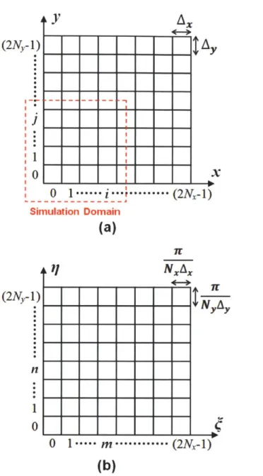
Figure 2.2: Pad surface deformation caused by applied pressure on wafer and retaining ring. ... 49 Figure 2.3: Discrete grid of the contact surface: (a) top view in space domain, (b)
Figure 2.7: Wafer-level pressure (psi) distributions of different pad thickness. ... 62 Figure 2.8: Pad thickness effect on wafer-level non-uniformity: (a) pressure
distribution along wafer radius; (b) pad surface displacement near
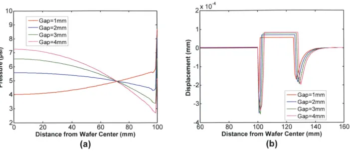
w afer edge. ... . 63 Figure 2.9: Wafer-level pressure (psi) distributions of different retaining ring
g ap s... . 6 4 Figure 2.10: Retaining ring gap effect on wafer-level non-uniformity: (a) pressure
distribution along wafer radius; (b) pad surface displacement near
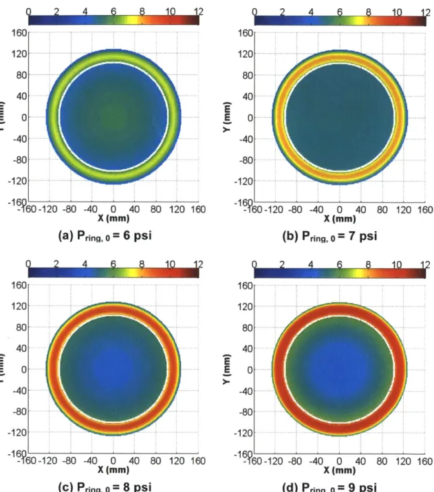
w afer edge. ... . 65 Figure 2.11: Wafer-level pressure (psi) distributions of different retaining ring
reference pressures. ... 66 Figure 2.12: Retaining ring pressure effect on wafer-level non-uniformity: (a)
pressure distribution along wafer radius; (b) pad surface displacement
near w afer edge. ... 67 Figure 2.13: Top view of the non-centered wafer position during the CMP
p ro cess ... . . 6 8 Figure 2.14: Instantaneous wafer-level pressure (psi) distributions of centered and
non-centered wafer position in the retaining ring. ... 69 Figure 2.15: Wafer position effect: radial time-averaged pressure distribution...69 Figure 2.16: Pad structure assumption in physical die-level CMP model. The
whole pad is comprised of bulk and asperities...71 Figure 2.17: Framework of physical die-level model: (a) wafer surface profile and
pad long-range deformation; (b) local step structures and pad asperity
com pression ... . 72 Figure 2.18: Discretization grid of the die-level model: (a) top view in spatial
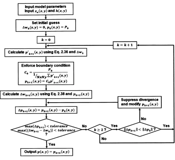
domain, (b) top view in frequency domain. ... 78 Figure 2.19: Flow chart of iterative program to calculate die-level pressure
distribution ... . . 80 Figure 2.20: Pattern type and pattern density within a die of SKW7-2 wafer: (a)
Layout of a die on SKW7-2 wafer (MIT standard oxide CMP
characterization layout). A "P" preceding a number indicates a pitch structure with 50% density, with the number following in microns. All other numbers are localized densities, with the number indicating the density. Density structures have a fixed 100 micron pitch. (b)
Figure 2.21: Pattern density (PD) dependence of CMP process: (a) Monitor sites in STEP arrays of MIT standard layout; (b) Up area thickness
evolution; (c) Step height evolution ... 84 Figure 2.22: Neighboring pattern density (pad long-range bending) effects of
CMP process: (a) Monitor sites in STEP arrays of MIT standard
layout; (b) Up area thickness evolution; (c) Step height evolution...85 Figure 2.23: Local planarization results of different pad bulk reduced moduli: (a)
Monitor site in 50% STEP array of MIT standard layout; (b) Step
height evolution; (c) Planarization efficiency evolution. ... 86 Figure 2.24: global planarization results of different pad bulk reduced moduli: (a)
Nominal range monitor sites; (b) Nominal range evolution...87 Figure 2.25: Local planarization results of different characteristic asperity heights:
(a) Monitor site in 50% STEP array of MIT standard layout; (b) Step
height evolution; (c) Planarization efficiency evolution. ... 88 Figure 2.26: Global planarization results of different characteristic asperity
heights: (a) Nominal range monitor sites; (b) Nominal range
ev o lution ... . 89 Figure 2.27: Active contact peaks of the surface profile on a glazed CMP pad
[84]: (a) Line scan; (b) Pad height probability distribution...90 Figure 2.28: CMP pad surface profile simplification: (a) define reference plane
and active parts of asperities; (b) find active asperities; (c) define active asperities as elastic posts; (d) define the shape of active post
h ead s... . . 92 Figure 2.29: A single asperity (active peak) being compressed. ... 93 Figure 2.30: Example of characteristic asperity height (A) extraction from
interferometry data of conditioned CMP pad [81]. ... 94 Figure 2.31: Pad-wafer contact percentage vs. applied reference pressure...97
Figure 2.36: Within-die local planarization results from different dies on the wafer: (a) Monitor site in 50% STEP array of a single die; (b) Step
height evolution of different dies. ... 103
Figure 2.37: Contact between asperities and features with 50% density on a chip: (a) large feature size; (b) sm all feature size. ... 105
Figure 2.38: Geometry of the contact between a pad asperity and a feature on the die [77]. Both shapes are assumed to be described by parabolic curves in the vicinity of the point of first contact...105
Figure 2.39: Pitch size effect in CMP: (a) Monitor sites in PITCH arrays (50% pattern density) of MIT standard layout; (b) step height evolution simulated by the extended die-particle-level model; (c) step height evolution simulated by the original die-level model...113
Figure 2.40: Asperity radius of curvature effect on planarization: (a) Monitor site in 50% STEP array of a single die; (b) Step height evolutions...114
Figure 2.41: Summary of physical CM P modeling. ... 115
Figure 3.1: IC design and manufacturing with assistance of CMP model...119
Figure 3.2: Measured die positions on an SKW7-2 dielectric polishing test wafer. ... 122
Figure 3.3: Measurement site positions in the STEP blocks in a die of SKW7-2 dielectric polishing test w afer...122
Figure 3.4: Extracted model parameters for different pad stiffnesses (low, standard, and high): (a) Effective modulus. (b) Characteristic asperity height. (c) B lanket rem oval rate. ... 124
Figure 3.5: Simulated middle die nominal range evolution for different pad stiffnesses: (a) Nominal range monitor sites; (b) Nominal range ev o lu tion ... 12 5 Figure 3.6: Middle die 50% pattern density array step height evolution for different pad stiffnesses (low, standard, and high): (a) Center point. (b) Left edge point (next to 70% pattern density array in Figure 3.3). (c) Right edge point (next to 10% pattern density array in Figure 3.3)...127
Figure 3.7: Extracted model parameters for different conditioning disk diamond shapes: (a) Effective modulus. (b) Characteristic asperity height. (c) B lanket rem oval rate. ... 129
Figure 3.8: Simulated middle die nominal range evolution for different conditioning disk diamond shapes: (a) Nominal range monitor sites; (b) N om inal range evolution. ... 130
Figure 3.9: Middle die 50% pattern density array step height evolution for different conditioning disks: (a) Center point. (b) Left edge point (next to 70% pattern density array in Figure 3.3). (c) Right edge point (next to 10% pattern density array in Figure 3.3)...131 Figure 3.10: Middle die 50% pattern density array center point step height versus
down area removal amount for different conditioning disk diamond shapes. Taking the down area removal amount at lnm as the linear to non-linear transition point, the remaining step heights of blocky, standard and sharp disks at the transition point are 436.Onm, 497.7nm, and 533.5nm , respectively...133 Figure 3.11: Full chip up area thickness (nm) evolutions of the SKW7-2 test
pattern polished by a JSR standard pad with conditioning of different disks: sharp, standard and blocky...135 Figure 3.12: Full chip step height (nm) evolutions of the SKW7-2 test pattern
polished by a JSR standard pad with conditioning of different disks: sharp, standard and blocky. The step height in the 100% density array is defined as our zero reference...136 Figure 3.13: Wafer-level step height evolution: (a) Die positions; (b) Monitor sites
in 50% pattern density array of each die; (c) Center monitor site in 50% pattern density array; (d) Left monitor site (next to 70% pattern density array); (e) Right monitor site (next to 10% pattern density array). Here "EXP" indicates experimental data, and "MOD" is the
fitted m o del...14 3 Figure 3.14: Extracted wafer-level pressure distribution for JSR pad with standard
stiffn e ss...14 4 Figure 3.15: Simulated nominal range evolutions for different die positions from
an SKW7-2 wafer polished by JSR standard pad...145 Figure 3.16: Simulated step range evolutions for different die positions from an
Figure 3.21: Up area thickness and step height evolutions of the 50% density region in the MIT standard STI CMP layout. Non-uniformity is
induced by the different pitch sizes arranged in this region...151 Figure 4.1: Figure 4.2: Figure 4.3: Figure 4.4: Figure 4.5: Figure 4.6: Figure 4.7: Figure 4.8: Figure 4.9:
Schematic diagram of a typical load vs. displacement curve in nanoindenation. The contact depth hc and slope of the elastic unloading dPdh allow specimen modulus and hardness to be
calculated. Here hr is the depth of the residual impression, he is the displacement associated with the elastic recovery during unloading, and ha is the displacement from the edge of the contact to the
specim en surface at full load...155 Indenter shape and geometry parameters [98]: (a) spherical, (b)
conical, (c) Vickers, and (d) Berkovich. ... 156 Hysitron TI 900 Tribolndenter [103]: (a) Chamber and controller; (b)
Sensor and optical microscope in the chamber. ... 157 Reduced modulus vs. indentation depth for Cabot 42D solid pad
material. Error bars represent one standard deviation of replicated
m easurem ents. ... 159 Conditioned pad sample nanoindentation: (a) asperity top indentation;
(b) test pattern of indents...160 Testing curves of conditioned pad sample nanoindentation: (a)
indenter tip sliding on asperity top; (b) solid contact between indenter
tip and asp erity . ... 160 Contact and non-contact methods of CMP pad surface profilometry
[107]: (a) Path of stylus over actual pad surface; (b) the pad surface as
'seen' by the white light interferom eter. ... 162 Asperity-wafer contact summit types in CMP: (a) fully supported; (b)
less well supported; (c) poorly supported...163 Extraction of characteristic asperity height: (a) Profilometry data. (b)
Probability density fitting of exponentially distributed heights...164 Figure 4.10: Sample collection from the polishing pad at different usage stages. ... 166 Figure 4.11: Pad asperity modulus vs. pad aging time. Error bars represent one
standard deviation across multiple indentation measurements in a 40
ptm by 40 pm indentation test region. ... 167 Figure 4.12: Characteristic asperity height vs. pad aging time. Error bars represent
Figure 4.13: Pad groove depth measurement with positioning control system on
n an o in d enter. ... 16 8 Figure 4.14: Pad groove depth vs. pad aging time. Error bars represent one
standard deviation...169 Figure 4.15: Contact percentage vs. pad aging time. Error bars represent one
standard deviation...170 Figure 4.16: TEOS removal rate vs. pad aging time. Error bars represent one
standard deviation...17 1 Figure 4.17: Spatial sample collection from the polishing pad after 16 hours
polishing/conditioning...172 Figure 4.18: Pad asperity modulus vs. sample locations. Error bars represent one
standard deviation: (a) OA direction in Figure 4.17. (b) OB direction
in F ig ure 4 .17 . ... 173 Figure 4.19: Characteristic asperity height vs. sample locations. Error bars
represent one standard deviation: (a) OA direction in Figure 4.17. (b) O B direction in Figure 4.17...174 Figure 4.20: Groove depth vs. locations on the pad after 16 hours
polishing/condition. Error bars represent one standard deviation...175 Figure 4.21: Reduced modulus vs. indentation depth for IC 1000 CMP pad...176 Figure 5.1:
Figure 5.2:
Figure 5.3:
The nature of CMP: polishing is the accumulated result of many
random m aterial rem oval events. ... 179 CMP with conventional polishing pad and novel pad-in-a-bottle [112]:
(a) polishing with polyurethane pad; (b) polishing with polyurethane beads as pad-in-a-bottle...180 Asperities vs. monosized polymer particles: (a) Surface of conditioned
Figure 5.6: Figure 6.1: Figure Figure Figure Figure Figure A.1: A.2: A.3: A.4: A.5: Figure A.6: Figure Figure Figure A.7: A.8: A.9:
Model approaches for pad-in-a-bottle: (a) Bead packing; (b) Bead
stack in g ... 18 5 Summary of the methodology of CMP modeling and physical
characterization . ... 193
Layout plan of the MIT STI CMP test mask...199
Pattern density arrangement of the MIT STI CMP test mask. ... 200
Arrangement of long-range pattern density structures. ... 201
Arrangement of bias structures and surrounding butter structures...203
Arrangement of dishing and erosion structures in 8 mm by 7 mm sub-reg io n ... 2 0 5 Arrangement of dishing and erosion structures in 7 mm by 9 mm sub-reg io n ... 2 0 9 Geometry parameters of rectangular structures...212
Geometry parameters of X-shape structures. ... 213
List of Tables
Table 1.1: Polishing factors attributed to physical CMP models...42
Table 2.1: Parameters used in the pitch size effect simulations. ... 112
Table 3.1: Experimental conditions for pad property studies...121
Table 3.2: Simulation results of step height target strategy for pad conditioning effects on JSR standard pad...138
Table 3.3: Simulation results of up area thickness target strategy for pad conditioning effects on JSR standard pad...139
Table 3.4: Wafer-level extracted model parameters and fitting errors for SKW7-2 wafer polishing with different pad stiffness (low, standard and high). ... 141
Table 3.5: Extracted model parameters for oxide polishing in STI CMP ex p erim en t. ... 14 9 Table 4.1: Geometry parameters for various types of indenters...157
Table A. 1: Geometry parameters of the long-range pattern density structures...201
Table A.2: Geometry parameters of the bias structures...202
Table A.3: Geometry parameters of the edge-acceleration structures...204
Table A.4: Geometry parameters of the structures in 20% density dishing and erosion sub-region. ... 206
Table A.5: Geometry parameters of the structures in 30% density dishing and erosion sub-region. ... 207
Table A.6: Geometry parameters of the structures in 70% density dishing and erosion sub-region. ... 208
1
Introduction
This thesis describes a set of physical modeling and characterization approaches to understand the mechanisms and variations in the chemical mechanical polishing (CMP) process for integrated circuit (IC) fabrication. In this chapter, background of CMP application in IC fabrication is first discussed in Section 1.1. Section 1.2 then briefly reviews the CMP tool and material removal mechanism. The key challenges in CMP are summarized in Section 1.3. Section 1.4 briefly categorizes existing CMP models, and Section 1.5 points out the need for advanced modeling and characterization for CMP process. The contributions of this thesis and the thesis structure are introduced in Section
1.6 and Section 1.7 respectively.
1.1
CMP background
The chemical mechanical polishing (CMP) process is one of the key enabling technologies required to continue the shrinking of devices and interconnect structures in silicon integrated circuit fabrication [1]. It is widely used in the front end process for device isolation, in the back end process for interconnection, and in new process integration approaches for building advanced device structures [2].
CMP was originally introduced to semiconductor fabrication in silicon wafer manufacturing in the 1960s to achieve flatness of the silicon wafer surface [3]. It was first used within IC manufacturing lines to achieve improved transistor isolation [4]. An important and necessary application of the CMP process in IC fabrication came with
1.1.1 CMP in inter-level dielectric planarization
For multilevel metal interconnects in very-large-scale integration (VLSI) technology, a key motivation for using CMP is to achieve planarity and to meet the stringent flatness requirements of the photolithography step. Although state-of-art photolithography tools are capable of refocusing after each exposure, extreme flatness with nanometer-scale height variations over a large chip area (about 20mmx2Omm) are desired, depending on the depth of focus (DOF) of the optics system. As the feature size of silicon IC structures decreases, the inter-level dielectric (ILD) planarity requirement
for CMP becomes even tighter [7].
Early CMP applications were largely driven by multilevel aluminum/oxide metallization schemes, together with tungsten vias and plugs. The SiO2 inter-level
dielectric planarization process flow is illustrated in Figure 1.1. The metal layer is first deposited; then the layer is patterned and etched to form desired structures; silicon oxide is deposited using conformal Chemical Vapor Deposition (CVD); lastly, the oxide layer is planarized using CMP. The global flatness allows an accurate photolithography step at each metal and via layer, and prevents topography from accumulating in the multilevel metal structures.
While copper has replaced aluminum in advanced IC fabrication, inter-level dielectric (ILD) CMP remains important in achieving planarity between the transistor formation and fabrication of multilevel copper interconnect. Furthermore, the basic mechanisms involved in single material CMP of SiO2 are key to understanding
AEA
(a) (b)
(c) (d)
Figure 1.1: Inter-level dielectric planarization process: (a) metal layer deposition, (b) metal pattern and etch, (c) SiO2 dielectric layer deposition, (d) SiO2 dielectric
layer CMP.
1.1.2 CMP in shallow trench isolation (STI)
Shallow trench isolation (STI) is the main isolation scheme for semiconductor manufacturing with active area pitches in the sub-0.25 tm regime [8]. STI is preferred because it has near zero field encroachment, good latch-up immunity, better planarity, and low junction capacitance. STI is also highly scalable, with the trench-fill capabilities being one major challenge to scaling. Figure 1.2 shows a typical STI process flow. First a thin pad SiO2 layer and a blanket Si3N4 film are deposited on a flat silicon wafer. The isolation trenches are etched such that the desired trench depth (depth from silicon surface) is achieved (typical depth is 500 nm). Then a thick SiO2 dielectric layer is
deposited to fill the trenches. The CMP process is used to polish the overburden SiO2
dielectric, down to the underlying nitride, where the nitride serves as a polishing stop " M
(a)
(C) (d)
Figure 1.2: Shallow trench isolation process: (a) pad SiO2 and Si3N4 deposition, (b) shallow trench etch, (c) CVD SiO2 trench fill, (d) CMP planarization.
1.1.3 CMP in damascene process for multilevel copper interconnection Multilevel copper interconnection is another critical element in advanced IC technologies [9]. CMP is the predominant fabrication technique because copper cannot be efficiently and cleanly dry-etched. There are several fabrication challenges in achieving high yield and economical copper wiring in key process steps including copper deposition, dielectric stack patterning, and planarization [10, 11]. Figure 1.3 illustrates a copper damascene process for interconnect. Trenches and vias are first patterned and etched within a low-k ILD stack. A thin layer of barrier material and copper seed layer are deposited. Then the copper wiring layer is electroplated from the seed. CMP is applied to remove excess copper and barrier material, leaving copper to form well-defined interconnect lines and vias.
(a)
(c) (d)
Figure 1.3: Damascene process of copper interconnection: (a) low-k dielectric trench and via etch; (b) barrier layer deposition; (c) copper interconnection layer plating;
(d) CMP planarization.
1.1.4 Other applications of CMP
The three typical examples above demonstrate the ability of CMP to planarize the wafer surface and to build multilevel structures. The combination of planarization and damascene approaches enables CMP to be used in microelectronic manufacturing whenever a high degree of planarization is demanded, or inlaid material and structures are desired. As new materials and complex devices are introduced in IC fabrication, CMP finds many new applications, such as building advanced transistor structures, nonvolatile memories, silicon-on-insulator (SOI) processes [2], wafer bonding [12], and others. In addition to being used to planarize the IC devices, CMP has also been applied in fabrication of MEMS devices [13-16]. The ability to achieve planarity and form inlaid
1.2 CMP process
This section provides an overview of how CMP is implemented and how wafer surface material is removed.
1.2.1 CMP tool
A schematic view of a rotary CMP tool is shown in Figure 1.4. A wafer is held on a wafer carrier such that the surface to be polished faces a polishing pad, which is typically made from porous polyurethane, attached to a rotating platen. The wafer carrier is rotated in the same direction as the pad, while being pressed against the pad. Slurry composed of abrasive particles suspended in a chemical solution is delivered on the pad during polishing, and is transported to the pad-wafer interface by the pad.
IF
Hollow Carrier Spindi Slurry Delivery
Wafer Carrier SluyF ... d codor
Pad Conditioner
Polishing Pad +- Polishing Platen
4 1 Hollow Platen Drive Spindle
CDP
Figure 1.4: Schematic view of a rotary type CMP tool [18].
In addition to rotary CMP tools, there are also linear CMP tools that use a rotating wafer carrier contacting a CMP pad moving on a linear belt [19]. However, the
fundamental mechanism of removal (wafer surface contact with a CMP pad, aided by CMP slurry particles and chemistry) is similar.
One key criterion in designing a CMP polishing system is a uniform and consistent polishing spatially and in time, and this is achieved via a collection of subsystems [18]:
a) A mechanical drive system is able to control the relative surface velocity at the target speed. Sometimes the relative velocity, however, is intentionally set to vary across the wafer to compensate for other wafer level non-uniformity.
b) A down force system controls pressure distribution across the wafer. One approach is to divide the wafer area into a few co-center zones and apply different pressure on different zones.
c) A thermal management system is used to provide a stable and uniform temperature distribution during CMP. Temperature affects chemical reactions and has significant impact on oxide polishing as well as metal polishing [20, 21]. A spatial temperature variation causes non-uniformity removal rate, and an unstable temperature during CMP can result in over-polishing or under-polishing.
d) A pad conditioning system regenerates/dresses the polishing pad surface to a working condition via either in-situ (during polishing) or ex-situ (between polishing) approaches. Conditioning keeps the pad surface in a stable functioning state to ensure that the CMP process produces consistent performance.
1.2.2 Material removal mechanism in CMP
CMP is a process that combines chemical reactions and mechanical forces in a synergistic way to remove surface materials and achieve desired planarity. It can be treated as chemically aided mechanical polishing, and material removal is believed to be primarily due to a three-body contact, as illustrated in Figure 1.5. First the wafer surface is modified and softened by the chemical solution, and the soft surface layer is removed by abrasive particles grabbed by the polishing pad. Without chemical modification, the wafer surface is too hard to be polished at appreciable rates; while without mechanical polishing, chemical modification and dissolution of the surface stops on its own (or does not activate planarization if it does proceed).
Pad Motion
.Fluid Abrasive
Particle
Wafer Motion
Figure 1.5: CMP material removal due to three-body contact.
In this simple picture, four components are involved: wafer surface, chemical solution, abrasive particles, and polishing pad.
a) Wafer surface is the object being polished, which can be a single material, such as silicon oxide or copper, or a mix of several materials, such as silicon oxide and silicon nitride in the later stages of the STI process.
b) Chemical solution is one of the main components of slurry. The chemical solution mixes and transports abrasive particles to the surface and carries wastes away
I A
from the surface. Another function of the chemical solution is to modify and soften the wafer surface, thus it usually has a high pH value for polishing dielectrics and a low pH value for polishing metals.
c) Abrasive particles, the other component of slurry, remove the softened surface materials. For dielectric polishing, the abrasives are typically made of silica or ceria; while for metal polishing, they are typically made of silica or aluminum. The size of abrasives ranges from 50 nm to a few hundred nanometers [22].
d) Polishing pad transports fresh slurry to the wafer surface and carries removed debris away. The pad is crucial for the mechanical part of CMP. When the pad grabs abrasive particles, the pad addresses higher pressure on raised wafer surface areas and thus produces a higher removal rate on raised features, which results in the planarization effect.
The material removal rate is often described by Preston's equation [23],
RR = K PV (1.1)
where RR is removal rate, K is a constant called Preston's coefficient, P is applied pressure on wafer surface, and V is relative velocity of the point on the surface of wafer versus the pad. Preston's equation is an empirical law first discovered in glass polishing. For most of the experiment results obtained in practice, especially in dielectric CMP, Preston's law provides a reasonably good fit. Preston's law suggests a linear dependence of removal rate on pressure and relative velocity; these contribute most of the mechanical
1.2.3 Schematic scales in CMP
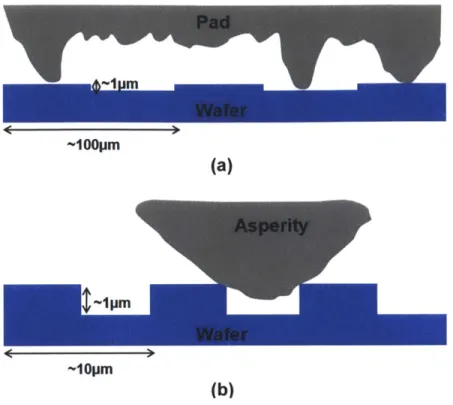
The CMP tool setup occurs over a macroscopic scale, for example, across an entire 300 mm wafer. However, material removal in CMP happens at a microscopic scale or even at a nanometer scale involving, for example, 30 nm abrasive particles. There is a 107 scale range between the two ends of these length scales. This subsection looks at the polishing behavior step by step across these orders of magnitude, as shown in Figure 1.6.
a) Tool scale (- 100 mm). The CMP system is set up in this range according to wafer size, typically 100 mm, 150 mm, 200 mm and 300 mm. Reference pressure and relative velocity are controlled in this level.
b) Pad-wafer contact scale (~ 1 mm). Polishing pad bending and surface texture affects local pressure on the wafer surface in this range. Pad asperity height distribution is an additional key factor affect contact area and localized pressures.
c) Abrasive trapping scale (~ 10 pm) is typically the contact area between the wafer and a single pad asperity. Slurry abrasive particles spread into the contact area and are trapped between the pad and wafer.
d) 3-body contact scale (~ 100 nm) is about a single abrasive particle size. The three interactive bodies are the wafer, abrasive particle and pad asperity. Wafer and particles are more rigid than a pad asperity, so that the main deformation is within the
asperity.
e) Material removal scale (~ Inm). Chemical reactions are of interest at this scale. Both wafer surface and abrasive particles are chemically modified. Deformation and material removal occur on both wafer surface and abrasive particles.
Schematic
Scale
I
m
100 mm
_
10mm
1 mm
_.
100pm
10 pm .1pm
.
100 nm -10 nm ./
F
_ _ _Tool
setup
WaferE
_Pad-wafer
contact
Abrasive-,-, - -
Abrasive trapping
L aicles
1.3 The challenges of CMP
CMP faces tremendous challenges in current and future IC technology nodes. Many of the challenges are not new; they have been with CMP since the beginning, but continued scaling drives increasingly stringent requirements with respect to these challenges. This section summarizes some of these major issues in the CMP process.
1.3.1 Challenge of within-die non-unformity
Pattern dependence is one of the main long lasting issues in CMP. The key definitions related to pattern dependence are the within-die non-uniformity (WIDNU), dishing, and erosion, which are heavily affected by layout pattern density and feature
size. In inter-level dielectric (ILD) polishing and other planarization applications, film thickness and step height variation control is very important for the following photolithography steps. Figure 1.7 illustrates the non-uniform polishing result induced by pattern density difference. After the conformal deposition process, step structures are formatted within ILD layer. High density regions have larger up area to contact the polishing pad, which results lower localized pressure. Therefore, high density regions are planarized slower than low density area. Thickness difference occurs between high density regions and low density regions, which is considered as the chip-scale global non-planarity. CMP engineers have to understand and characterize pattern dependence properly so that they can modify the layout design rules and optimize the process to
No planarization
Before
CMP
High density Low density
Local planarization
After non-planarity
CMP
High density Low density
Figure 1.7: Pattern dependence in ILD CMP.
Dishing and erosion are two pattern dependent concerns in both STI CMP [24] and copper CMP [25, 26]. In STI CMP, dishing refers to the oxide loss relative to the level of the neighboring nitride space, and erosion refers to the nitride loss relative to the nitride level of the neighboring area. In copper CMP, dishing is defined as the copper loss relative to the level of the neighboring dielectric space, and erosion is the dielectric loss relative to the dielectric level of the neighboring area. Figure 1.8 shows dishing and erosion in copper CMP. Wide trenches or open structures usually have significant
Before
CMP
Small line Large line Small line Large line Small space Large space Large space Small space
Local
Dishing
planarization
LocalcopperlossAfter
CMP
Small line Large line Small line Large line Small space Large space Large space Small space
Figure 1.8: Pattern dependence in copper CMP.
1.3.2 Challenge of within-wafer non-uniformity
Another critical challenge in CMP is within-wafer non-uniformity (WIWNU) of material removal, which reduces the yield of the process [27]. The WIWNU also brings a systematic variation of the chip performance across the whole wafer. A proper understanding of the drives of WIWNU is important for the CMP process, in order to increase yield and improve chip quality. The WIWNU can be caused by non-uniform distributions of velocity and pressure from the polishing tool; consumable effects, such as polishing pad material, pad topography and slurry abrasive size distribution, and slurry flow non-uniformity, can also become sources of wafer level variation.
1.3.3 Other challenges
Within-die non-uniformity (WIDNU) and within-wafer non-uniformity (WIWNU) as discussed above are only two examples of CMP problems. There are other continuing
and growing challenges in CMP, such as defect rate, consumable cost, waste disposal, tool maintenance and environmental issues. CMP research is a wide area, and understanding of critical CMP issues is important for continued improvement of the process. Today's CMP is a jigsaw puzzle shown in Figure 1.9. Each new material process or new process integration approach usually requires a new CMP process, or at least solving a CMP jigsaw puzzle using known recipes. Every single piece in the puzzle may be a challenge under specific conditions in future development of IC processes. In Section 1.6, we identify the parts of this puzzle that this thesis seeks to address.
1.4 CMP models
Various CMP models are proposed in the literature to help understanding and improving the CMP process. According to the scale and usage in practice, they can be categorized into one of the three levels: particle-level, die-level and wafer-level.
1.4.1 Particle-level CMP models
Particle-level models seek to understand the material polishing mechanism of CMP and find the dependence of output variables, such as removal rate and surface quality [29, 30], on various input variables, such as applied pressure, chemical pH, abrasive size, and other consumable or process parameters. Physical understanding of the basic CMP mechanism enables better design and control of the process [31].
In particle-level models, CMP is usually studied in an ideal scenario: blanket wafer with single material, uniform chemical concentration, uniform abrasive size, etc. [32, 33]. Physical understanding can be approached empirically by isolating a few input and output variables and analyzing their dependence [34, 35], or theoretically by deriving models from basic physical assumptions [36, 37]. A particle-level model can also serve as the foundation to build die-level and wafer-level models.
1.4.2 Die-level CMP models
Die-level models focus on the planarization part of CMP, and study the polishing of one or more structures with known geometric shapes, at different locations within a chip or die, or across the entire die [38-40]. Dealing with a simple case, die-level models are able to focus in detail on how the existing structure features are planarizaed by modeling the transportation of CMP slurry chemicals and abrasives, pressure distribution, and/or other factors [41, 42]. In a real product die, however, there are millions to billions of individual structures; therefore modeling each of them separately is not feasible. Die-level models usually resort to statistical terms to describe and analyze the problem [18, 26, 43]. Die-level models often make assumptions such as uniform slurry flow across the
wafer, and benefit from the boundary condition that dies are arranged periodically on the wafer.
Die-level models help process engineers estimate process windows, identify potential weak spots of the polished chip, and modify CMP setup to improve the process.
The models are particularly useful at the layout design stage. Chip designers can make their designs more fab-friendly with the feedback provided by these models, so that cost can be saved. This "Design for Manufacturing" (DFM) concept has been well adopted in the semiconductor manufacturing industry.
1.4.3 Wafer-level CMP models
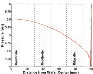
Wafer-level models try to address the cases when the assumptions in die-level models fail due to tool limitations, such as non-uniform distribution of pressure [44, 45], slurry concentration [46, 47], and temperature [48]. Pressure distribution is highly non-uniform near the wafer edge, which results in a typical roll-off profile. Another cause of non-uniformity is that the dies near the wafer edge do not have some of their neighboring dies, resulting in different environments on the edge die. Slurry is a critical component of the CMP process; however, an even delivery of slurry across the wafer is difficult to achieve, which causes non-uniform slurry concentration [49]. Slurry transportation also has the effect of temperature cooling, and its variation can cause non-uniform temperatures across the wafer [50]. Wafer-level models help the tool manufacturers to design better polishing tools as well as help process engineers to better control the CMP process [51, 52].
parameters in these models are usually coupled with mixed process inputs, and it is not easy to separate and identify processing parameter effects based on empirical models. Another main motivation of modeling is to refine the designs on both the CMP user end (chip layout) and the CMP vendor end (CMP consumables). A successful CMP model should consider inputs from both ends and including parameters with physical meaning. Therefore, physically-based CMP models are eagerly desired.
CMP model development is generally focused on the particle-level, die-level or wafer-level. However, model simulation should not be limited to a single level. Multilevel model integration is needed to consider more effects, to understand the
interaction between levels, and to make better polishing result predictions.
Physical characterization is required to verify model assumptions and test model reliability, especially for the models including consumable properties. A series of characterization approaches needs to be developed and applied.
1.6 Contributions of this thesis
This thesis contributes to both physical modeling of the CMP process, and to applications of these models. Physical measurement approaches are developed to characterize CMP pad properties and to verify model assumptions.
1.6.1 Developing physical CMP models
In this thesis, physical models are developed at three levels: wafer-level, die-level and particle-level. While the modeling approach is applicable to both dielectric and metal CMP, our work focuses on oxide polishing.
a) Wafer-level model. The within-wafer non-uniformity of the material removal rate has long been a concern in CMP, because wafer-level pressure distribution is non-uniform. We propose a physical wafer-level CMP model based on contact mechanics to address the pressure non-uniformity due to the polishing tool geometry, retaining ring
shape, and polishing pad properties. This model can be used to simulate blanket wafer polishing, or integrated with die-level models to simulate the implications on patterned wafer polishing.
b) Die-level model. In CMP process studies, an urgent need is to understand pattern density effects and to evaluate planarization performance at the chip scale. We adopt an explicit framework for die-level modeling of CMP, which abstracts the layout with of different pattern densities. Polishing performance is established by considering force responses from both the CMP pad bulk and from pad asperities. Pad properties are taken as model parameters. This model offers a potential characterization method for pad modulus and conditioning effect.
c) Particle-level model. A particle-level model is proposed to study the interaction between wafer surface and pad asperities using a Greenwood-Williamson approach [53].
Two main asperity properties are included in the model: asperity reduced modulus and asperity height distribution. Contact area percentage between the wafer and pad during CMP can be predicted. This model can be partly integrated into the physical die-level model to consider feature size effects.
The three single level models come together to help solve a simplified CMP jigsaw puzzle containing four key factors of the CMP process, as shown in Figure 1.10. The four factors of pad parameters, conditioning, applied pressure, and pattern dependency effects are attributed to the three levels based on the scale of interest and computational complexity, as listed in Table 1.1. Conditioning effects are addressed through impact on
Simplified CMP Jigsaw Puzzle
4
Figure 1.10: A simplified CMP jigsaw puzzle solved by the modeling work of this thesis.
Table 1.1: Polishing factors attributed to physical CMP models.
Pattern density Pressure Pad modulus Conditioning
Wafer-level No Yes Yes No
Die-level Yes Yes Yes Yes
Particle-level No Yes Yes Yes
Two extended die-level models are developed by integrating the three single level models in this thesis:
a) Extended wafer-die-level model including wafer-level non-uniformity. This model is derived by integrating the wafer-level model and the die-level model. Wafer-level pressure non-uniformity is implanted in the die-Wafer-level model as the pressure boundary condition, so that CMP tool wafer-level impacts on die-level non-uniformity can be considered.
b) Extended die-particle-level model including feature size effect. This model is derived by integrating die-level model and particle-level model. Asperity shape is
considered when we calculate the contact pressure between asperity top and chip feature structure, so that asperity shape impact on feature size dependence of planarization is addressed.
1.6.2 Applying physical CMP models
Four engineering applications of the physical CMP models are demonstrated, together with our modeling methodology consisting of polishing experiments on standard testing wafers, model calibration (model parameter extraction), and model prediction (simulations with calibrated models).
a) Model characterization of CMP pad properties. Patterned oxide wafers are polished using CMP pads with intentionally modified bulk and surface properties. Physical die-level model is used to fit the polishing results and extract model parameters. CMP pad properties are related to model parameters. The effect of pad stiffness and conditioning disk diamond shape are investigated.
b) CMP end-point strategy and within-die non-uniformity study. Full chip model simulations are performed under two different end-point strategies: step height target strategy and up-area thickness target strategy. At each end-point, within-die non-uniformity is estimated.
c) Evaluation of within-wafer non-uniformity impact on die-level planarization. The extended wafer-die-level model is fit to patterned oxide wafer polishing results. Wafer-level pressure non-uniformity during polishing process is verified, and
1.6.3 Physical characterization of CMP pad properties
In CMP, pad asperity modulus and asperity height distribution are two important properties that affect planarization. The coefficients of these two pad properties, asperity modulus and characteristic asperity height, are employed as CMP model parameters to understand polishing performance in this thesis. A physical CMP pad characterization approach based on nanoindentation and microprofilometry is demonstrated for pad surface property studies to verify underlying model assumptions.
Pad aging is an important factor in CMP, as typical processes suffer lot-to-lot, or even wafer-to-wafer, removal rate decay due to aging. A physical characterization approach is applied to evaluate pad aging effects. A pad aging experiment is run by polishing blanket oxide wafers up to 16 hours with in-situ conditioning. At different stages of this marathon test, physical characterization is performed at the same location on the pad and the measured results are compared. The measured asperity modulus and asperity height are applied in the particle-level CMP model to predict pad-wafer contact percentage.
1.6.4 Physical modeling of "pad-in-a-bottle"
The "pad-in-a-bottle" (PIB) approach to CMP is essentially a bottle of polymer beads which have similar chemical and mechanical properties as a polishing pad. The approach is hypothesized to be able to perform CMP by mixing in slurry to provide force response, so that no traditional pad is needed. Inspired by our particle-level model prediction and physical characterization, we know polishing is an accumulation of single material removal events, which we conjecture can be achieved by pad-in-a-bottle approach even in the absence of a traditional CMP pad. Therefore, we propose a simple physical model to study the behavior of the pad-in-a-bottle approach and estimate the relationship of applied pressure and material removal rate in this variant of CMP.
1.7 Thesis structure
The remainder of this thesis has the following structure. Chapter 2 develops basic physical CMP models at three levels: wafer-level, die-level and particle-level, and presents two approaches to model integration to extend the die-level model. Chapter 3 presents physical model applications including model characterization of CMP pad properties, CMP end-point prediction, evaluation of wafer-level non-uniformity impact on die-level planarization, and verification of feature size dependence of patterned wafer CMP. Chapter 4 demonstrates two physical measurement approaches to characterize CMP pad properties. Pad aging effects are evaluated based on these measurements. Chapter 5 proposes a physical modeling approach for CMP with "pad-in-a-bottle". Finally, Chapter 6 concludes and suggests area for future research.
2 Physical modeling of CMP
In this thesis, we believe there is a high priority CMP modeling need at die-level for CMP users in the IC industry [39, 40, 54-57]. The within-die non-uniformity (WIDNU) is a major concern for both layout designers and process engineers. A die-level CMP model seeks to simulate the planarization of layout structures on a chip and predict the polished chip surface profile. Such a capability would provide layout designers with a way of making optimized pattern arrangements to realize a uniform polishing result. On the other hand, a die-level model would help CMP process engineers to choose an appropriate set of process parameters (such as pressure, conditioning force, CMP pad hardness, etc.) for a given layout design. Furthermore, a good die-level model should be compatible with wafer-level models and particle-level models for extended applications. Therefore, our core modeling is focused on the die-level, while our wafer-level and particle-level models provide inputs for better die-level predictions.
In this chapter, we first take a top-down view to introduce our physical CMP models at the wafer-level, die-level and particle-level. Then we extend the die-level model to include wafer-level or particle level effects. For convenience in mathematical representation, this chapter takes the positive Z-axis to correspond to a surface normal up through the face of the wafer; this gives the appearance of a "wafer face up" convention in all model derivations although we note that in most CMP processes, the wafer face is pressed downward into the polishing pad.
schematically shows the geometry near the wafer edge. The wafer is surrounded by a retaining ring, which is usually a few millimeters away from the edge of the wafer. In a typical setting, different pressures are applied to the wafer and the ring, with the ring usually under higher pressure to prevent the wafer from slipping out. The pad bends around the wafer edge due to the existence of the gap and retaining ring, thus the wafer edge is polished non-uniformly due to a localized pressure affected by the retaining ring. The factors affecting the non-uniform pressure include pad modulus, pad thickness, retaining ring size, and reference pressures on the wafer and retaining ring. To understand the details, a physical wafer-level CMP model is developed based on contact mechanics. Retaining ring shape and CMP pad thickness effects are captured in the model.
Down Force Retaining Ring
Wafer,
(a)
(b)
Figure 2.1: Wafer carrier configuration of CMP: (a) Wafer surrounded by retaining ring. (b) Pad deformation around wafer edge.
2.].1 Model derivation
We first investigate the "thick pad" case: the applied pressure is low and the pad deflection is much smaller than the pad original thickness. The polishing pad thickness can be assumed to be infinite. We begin by adopting an analytical model based on the Boussinesq-Cerruti integral equations [58]. The roughness of contact surfaces is not considered. The CMP pad is assumed to be soft, while wafer and retaining ring are assumed to be rigid, so that only pad deflection needs to be calculated. The wafer and retaining ring sit are pressed into the pad with controllable applied reference pressures
Pwafer,o and Pringo, as shown in Figure 2.2. Here z(x, y) is the profile of the rigid surfaces, both wafer and retaining ring. The deflected pad topography w(x, y) and the contact pressure p(x, y) are both defined as positive up into the pad material.
z
(X,
)w
(x, y)
Pwafer
o
Pring oFigure 2.2: Pad surface deformation caused by applied pressure on wafer and retaining ring.